Lab 4: Cell-Based ASIC Implementation Flow Copyright (c) 2000 Dept. of Electronics, Carleton University. Material from "Tutorial on CMC’s Digital IC Design Flow", Copyright (c) 2000 Canadian Microelectronics Corporation, used with permission. This tutorial involves the use of documentation, software and technology database files. Ensure you understand the conditions governing the use of all licensed material.
Transcript
Lab 4:Cell-Based ASIC
Implementation Flow
Copyright (c) 2000 Dept. of Electronics, Carleton University.
Material from "Tutorial on CMC’s Digital IC Design Flow",Copyright (c) 2000 Canadian Microelectronics Corporation,
used with permission.
This tutorial involves the use of documentation, software and technology databasefiles. Ensure you understand the conditions governing the use of all licensedmaterial.
16 August 2002 9:20 am MODULE 1: INTRODUCTION
This sections describes what the manual is about. It outlines the design methodology used, and gives a description ofthe design example used in the tutorial. The conventions used in the manual are also described.
MODULE 1: INTRODUCTION❒ Introduction, Design Example and Manual Conventions ❒
Simulation
Synthesis
LibrariesConstraints
VHDL orVerilog
Copyright 2000 Dept. of Electronics, Carleton University Page 1-4
16 August 2002 9:20 am MODULE 1: INTRODUCTION
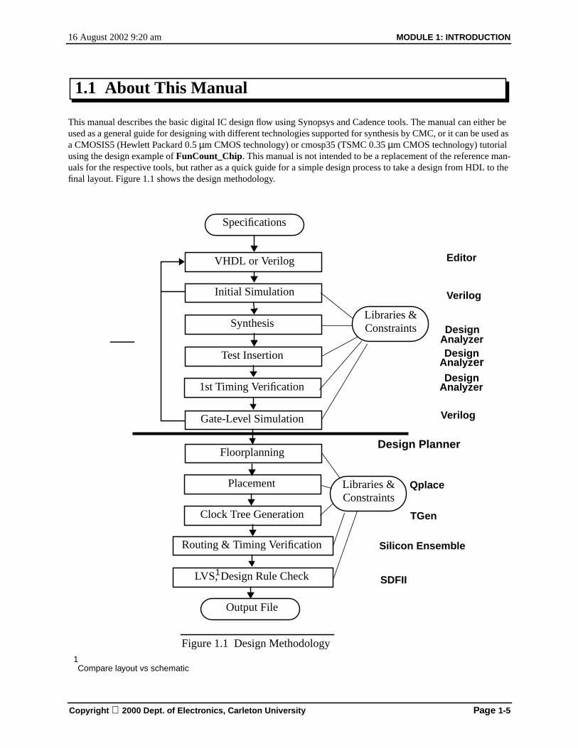
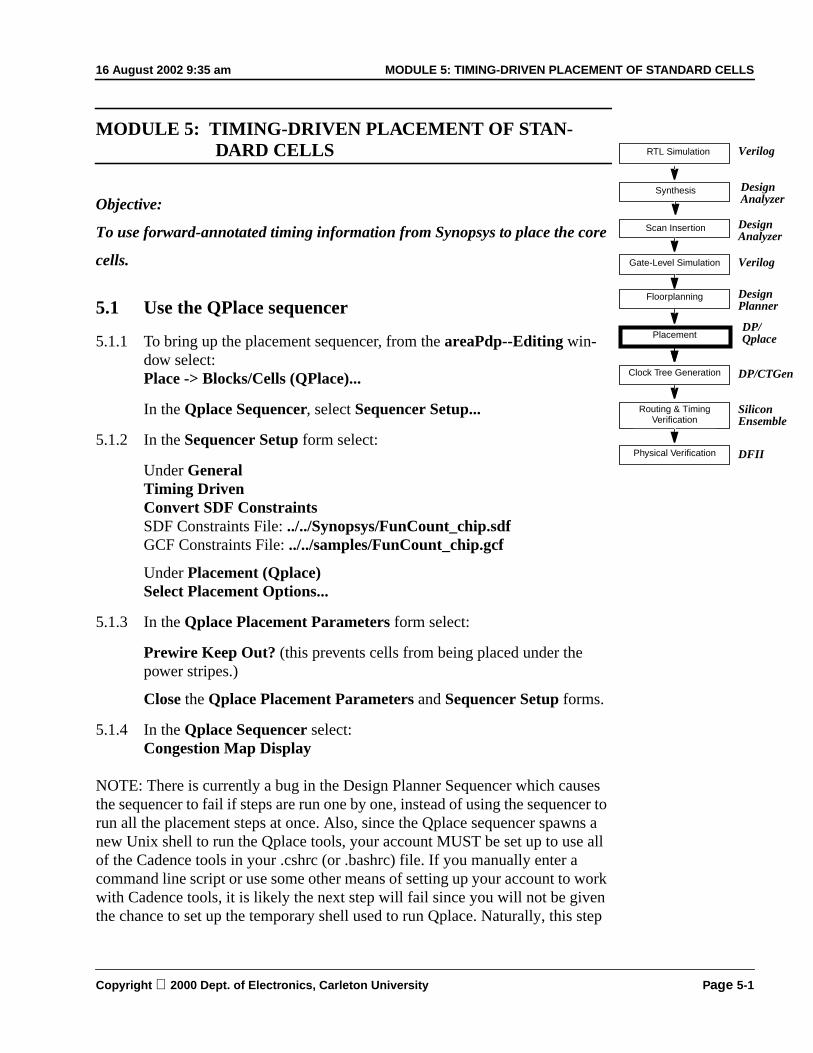
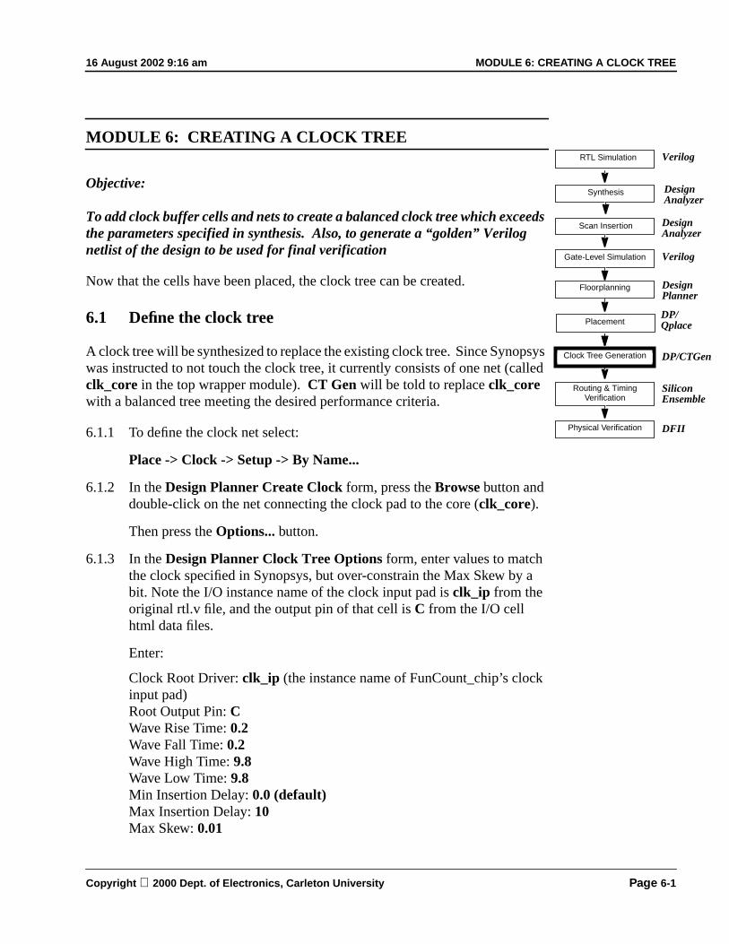
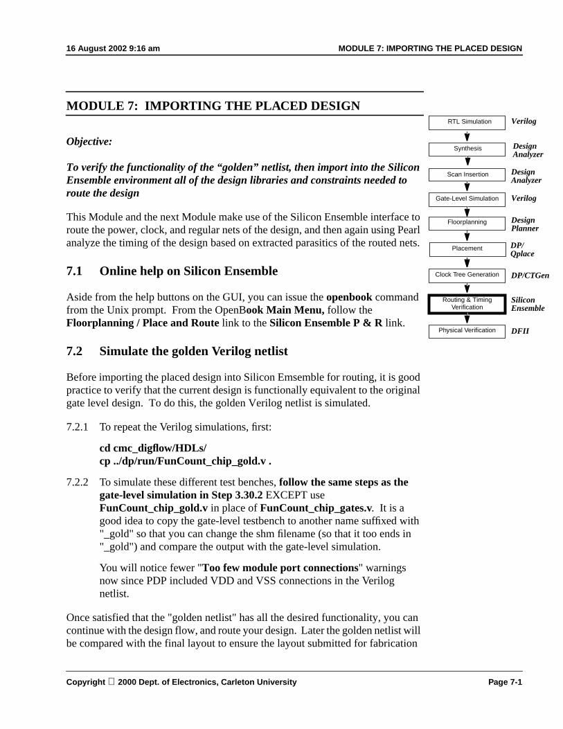
This manual describes the basic digital IC design flow using Synopsys and Cadence tools. The manual can either beused as a general guide for designing with different technologies supported for synthesis by CMC, or it can be used asa CMOSIS5 (Hewlett Packard 0.5 µm CMOS technology) or cmosp35 (TSMC 0.35 µm CMOS technology) tutorialusing the design example of FunCount_Chip. This manual is not intended to be a replacement of the reference man-uals for the respective tools, but rather as a quick guide for a simple design process to take a design from HDL to thefinal layout. Figure 1.1 shows the design methodology.
1.1 About This Manual
Specifications
Initial Simulation
Test Insertion
Gate-Level Simulation
Floorplanning
Clock Tree Generation
VHDL or Verilog
Libraries &Constraints
Output File
Figure 1.1 Design Methodology
Verilog
Design Planner
DesignAnalyzer
Verilog
Editor
Synthesis
1st Timing VerificationDesign
Analyzer
DesignAnalyzer
Placement
Routing & Timing Verification
LVS, Design Rule Check
Qplace
TGen
Silicon Ensemble
SDFII
Libraries &Constraints
Compare layout vs schematic1
1
Copyright 2000 Dept. of Electronics, Carleton University Page 1-5
16 August 2002 9:20 am MODULE 1: INTRODUCTION
The following conventions are used in the manual.
1.2 Manual Conventions
1.2.1 Italicized Variables
In a command ora parameter field, these represent vari-ables that should be replaced by the actual objects inyour design:
e.g. command to be executed:elaborate module
description of module, and object that should replacemodule in the above command are given as follows:
moduleThe module name of the Verilog model. If the design
contains more than one module, elaborate eachmodule separately.
i.e, for the tutorial, the above command should be exe-cuted as:elaborate accum
1.2.2 Errors, Warning, and Reports
This box describes the various errors, warnings, andinformation that you might encounter when executingthe step. It also describes possible solutions. If you geterrors/warnings, read the info in this box before con-sulting the TA/Professor.
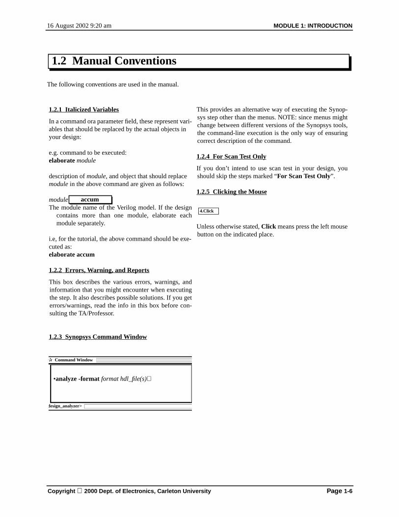
1.2.3 Synopsys Command Window
accum
✰ Command Window
•analyze -format format hdl_file(s)↵
design_analyzer>
This provides an alternative way of executing the Synop-sys step other than the menus. NOTE: since menus mightchange between different versions of the Synopsys tools,the command-line execution is the only way of ensuringcorrect description of the command.
1.2.4 For Scan Test Only
If you don’t intend to use scan test in your design, youshould skip the steps marked “For Scan Test Only”.
1.2.5 Clicking the Mouse
Unless otherwise stated, Click means press the left mousebutton on the indicated place.
4.Click
Copyright 2000 Dept. of Electronics, Carleton Uni
versity Page 1-6
16 August 2002 9:20 am MODULE 1: INTRODUCTION
In this step you setup the synthesis and simulation design environment by using the Synopsys setupfiles. Some of the variables that need to be specified before you can run synthesis and gate-levelsimulation include the technology and symbol libraries of the target technology, gate-levelsimulation libraries, as well as the search path to these and other libraries and design references.
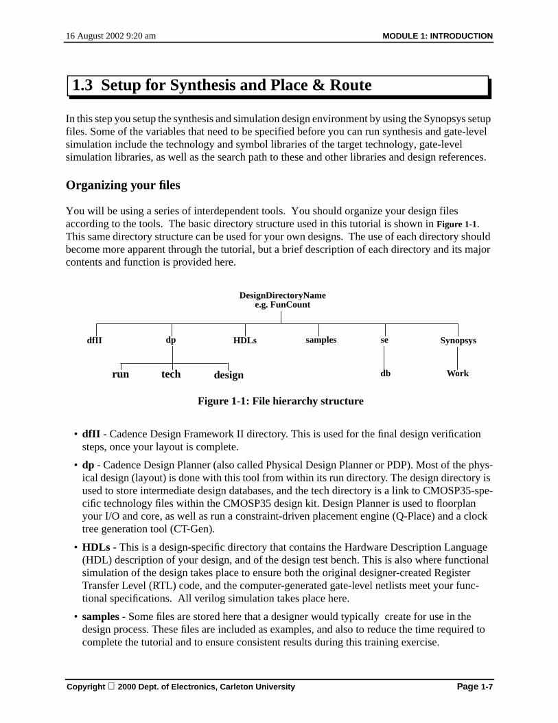
Organizing your files
You will be using a series of interdependent tools. You should organize your design filesaccording to the tools. The basic directory structure used in this tutorial is shown in Figure 1-1.This same directory structure can be used for your own designs. The use of each directory shouldbecome more apparent through the tutorial, but a brief description of each directory and its majorcontents and function is provided here.
• dfII - Cadence Design Framework II directory. This is used for the final design verificationsteps, once your layout is complete.
• dp - Cadence Design Planner (also called Physical Design Planner or PDP). Most of the phys-ical design (layout) is done with this tool from within its run directory. The design directory isused to store intermediate design databases, and the tech directory is a link to CMOSP35-spe-cific technology files within the CMOSP35 design kit. Design Planner is used to floorplanyour I/O and core, as well as run a constraint-driven placement engine (Q-Place) and a clocktree generation tool (CT-Gen).
• HDLs - This is a design-specific directory that contains the Hardware Description Language(HDL) description of your design, and of the design test bench. This is also where functionalsimulation of the design takes place to ensure both the original designer-created RegisterTransfer Level (RTL) code, and the computer-generated gate-level netlists meet your func-tional specifications. All verilog simulation takes place here.
• samples - Some files are stored here that a designer would typically create for use in thedesign process. These files are included as examples, and also to reduce the time required tocomplete the tutorial and to ensure consistent results during this training exercise.
1.3 Setup for Synthesis and Place & Route
dfII HDLs samples se Synopsysdp
run designtech Workdb
Figure 1-1: File hierarchy structure
DesignDirectoryNamee.g. FunCount
Copyright 2000 Dept. of Electronics, Carleton University Page 1-7
16 August 2002 9:20 am MODULE 1: INTRODUCTION
• se - Silicon Ensemble directory. Silicon Ensemble is a powerful set of tools, many of whichcan also be called from the Design Planner tool. For the purpose of this flow, the SiliconEnsemble tool is used for constraint-based routing of your design, and for running the Pearlstatic timing analyzer to ensure your routed design meets your timing constraints.
• Synopsys - This directory is used for synthesis to convert your design from RTL code intogate-level code, generate timing constraints to be met by the placement and routing tools, andto create scan-based test and test vectors. It contains a .synopsys_dc.setup file which points totechnology-specific standard cell libraries (the black-box libraries) and a Work sub-directorythat contains working views of your design.
Example Design for Synthesis and Place & Route: A Funny Counter
The top module of the design example is FunCount_chip_RTL.v. This is a 3-bit counter (or statemachine) that cycles through the number 0 to 7 (i.e. 8 states), but not in the numerical order to thosestates. It is a simple state machine that is broken into combinational part and sequential part (checkyour Verilog notes for how to implement a state machine). The RTL code is divided among twofiles. The core functionality (combinational and sequential parts) are contained in a file namedFunCount_core_RTL.v, while FunCount_chip_RTL.v contains the top wrapper module thatinstantiates this core and puts I/O buffer pads along its ports. The reasons for this partitioning aredescribed in Step 3.8.
See your HDLs subdirectory for FunCount_chip_RTL.v, FunCount_core_RTL.v and (the testbench) TB_RTL.v.
It is worthwhile to note that the example of this tutorial is quite fictitious in that it is an I/O bounddesign i.e. the area required by the functional core is much smaller than the area encompassed bythe ring of I/O pads. This design would not normally be fabricated because much of the areaencompassed by the I/O pad ring is wasted. Furthermore, the number of power pads are chosenarbitrarily. In reality, analysis and simulation are required to ensure that the power supply isadequate (e.g. the power usage report in Synopsys synthesis), but not overkill.
Startup Files for Synthesis and Place & Route
In addition to example design files, there are startup parameters for the tools themselves, some ofwhich are “hidden” files i.e. file with names beginning with “.” will only be listed using thecommand “ls -A”.
• design_analyzer: “.synopsys.dc_setup” in the Synopsys directory contains startup informa-tion for Synopsys Design Analyzer and Test Compiler. The file for this lab follows CMC’stutorial. This slightly complicates the testbench modifications for the synthesized design, asyou will see in Step 3.30.
• areaPdp: The dp directory contains a soft link tech to a cell library which must be dupli-cated, while the directory dp/run contains a local.dpux for the placement tool “areaPdp”.
• Silicon Ensemble: The se directory has initialization file se.ini for Silicon Ensemble routingtools.
Copyright 2000 Dept. of Electronics, Carleton University Page 1-8
16 August 2002 9:20 am MODULE 1: INTRODUCTION
All of these files are required for the tools to run. When you duplicate the file hierarchy structureto work on your own design, you should copy these files as well. In addition, the followingexample files are provided as a guide and need not be copied when you duplicate the file trees fora designs other than in this lab.
• The samples directory contains a template file FunCount_chip.gcf that serves as a an exam-ple of how to pass some key information to areaPdp for timing analysis.
• The Synopsys directory contains a ScriptCommands.da, the Design_Analyzer commands tosynthesize the funny counter.
This tutorial would not be possible without contribution of Canadian MicroelectronicsCorporation’s document for their Tutorial on CMC’s Digital IC Design Flow V1.1. The Cadenceportion of this tutorial consists of minor modifications of CMC’s document, and swaths of theSynopsys portion have been transplanted to here. CMC’s tool flow tutorial is quite expansive, soa good portion related to layout verification is not included in this general digital design coarse.Special thanks goes to Brent Veitch, Gail Burgess, and others at CMC who created the documentand made it accessible, and patiently provided consultation on the problems whose solutions werealready explained therein. Finally, acknowledgement is owing to Peter Nyasulu who, togetherwith Professor John Knight, originated the document on which the Synopsys part of this tutorial isbased.
1.4 Credits
Copyright 2000 Dept. of Electronics, Carleton University Page 1-9
16 August 2002 9:31 am MODULE 2: SIMULATE THE VERILOG RTL MODEL
In this step you verify the functionality of the Verilog behavioral model by simulating it using Cadence Verilog-XLSimulator. You can print the results of the simulation (in text format) using the in-built Verilog system tasks, or youcan view the signals waveforms using SignalScan waveform viewer.
MODULE 2: SIMULATE THE VERILOG RTL MODEL❒ Verify the Functionality of the RTL Model ❒
always @(posedge clk)begin c = a & b;end
c
b
clk
Copyright 2000 Dept. of Electronics, Carleton University Page 2-10
16 August 2002 9:31 am MODULE 2: SIMULATE THE VERILOG RTL MODEL
Make a Lab4 directory within your working directory. Since you could very well make multiple attempts at the designflow, create another directory within Lab4 called Try1, or TueAug27_3pm (whatever the date/time is), or whatevername you find most helpful. From within this last directory, issue the command
cp -r ~gallan/vitesse/FunCount_StartTree/* .
to copy the file tree and startup files of Step 1.3 to Try1 (assuming that’s the directory name you chose). Then copyyour RTL design files and RTL testbench to the HDLs subdirectory. Go to the HDLs directory now.
You should go through the Verilog source files in your HDLs subdirectory using any editor you prefer (vi, pico,emacs or...etc). Try to understand the code of the two modules of the “Fun Counter” (i.e. FunCount_core andFunCount_chip). Understanding the code not only will help you understand the output waveforms, but also willgive you an idea about the Black boxes and/or standard cells that this Counter is going to synthesize to in the nextstage.
2.1 Revise the RTL Design
Copyright 2000 Dept. of Electronics, Carleton University Page 2-11
16 August 2002 9:31 am MODULE 2: SIMULATE THE VERILOG RTL MODEL
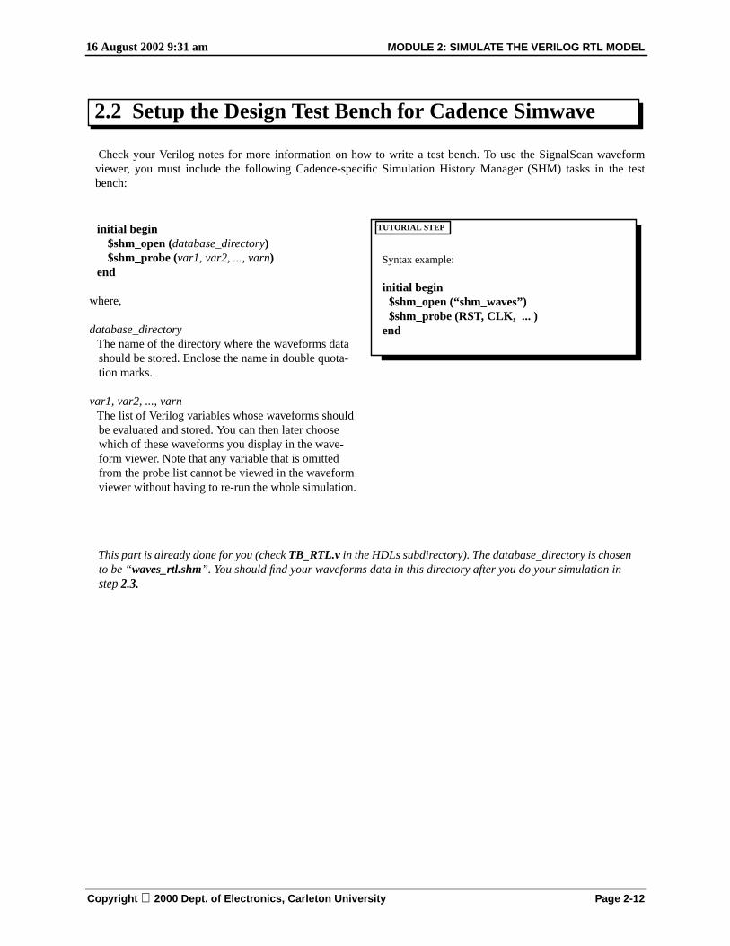
Check your Verilog notes for more information on how to write a test bench. To use the SignalScan waveformviewer, you must include the following Cadence-specific Simulation History Manager (SHM) tasks in the testbench:
2.2 Setup the Design Test Bench for Cadence Simwave
database_directoryThe name of the directory where the waveforms datashould be stored. Enclose the name in double quota-tion marks.
var1, var2, ..., varnThe list of Verilog variables whose waveforms shouldbe evaluated and stored. You can then later choosewhich of these waveforms you display in the wave-form viewer. Note that any variable that is omittedfrom the probe list cannot be viewed in the waveformviewer without having to re-run the whole simulation.
TUTORIAL STEP
This part is already done for you (check TB_RTL.v in the HDLs subdirectory). The database_directory is chosento be “waves_rtl.shm”. You should find your waveforms data in this directory after you do your simulation instep 2.3.
Copyright 2000 Dept. of Electronics, Carleton University Page 2-12
16 August 2002 9:31 am MODULE 2: SIMULATE THE VERILOG RTL MODEL
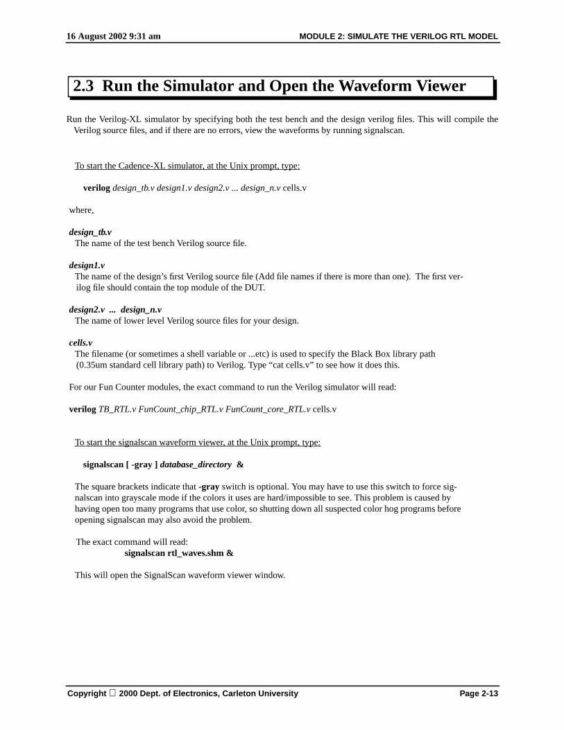
Run the Verilog-XL simulator by specifying both the test bench and the design verilog files. This will compile theVerilog source files, and if there are no errors, view the waveforms by running signalscan.
2.3 Run the Simulator and Open the Waveform Viewer
To start the Cadence-XL simulator, at the Unix prompt, type:
design_tb.vThe name of the test bench Verilog source file.
design1.vThe name of the design’s first Verilog source file (Add file names if there is more than one). The first ver-ilog file should contain the top module of the DUT.
design2.v ... design_n.vThe name of lower level Verilog source files for your design.
cells.vThe filename (or sometimes a shell variable or ...etc) is used to specify the Black Box library path(0.35um standard cell library path) to Verilog. Type “cat cells.v” to see how it does this.
For our Fun Counter modules, the exact command to run the Verilog simulator will read:
To start the signalscan waveform viewer, at the Unix prompt, type:
signalscan [ -gray ] database_directory &
The square brackets indicate that -gray switch is optional. You may have to use this switch to force sig-nalscan into grayscale mode if the colors it uses are hard/impossible to see. This problem is caused byhaving open too many programs that use color, so shutting down all suspected color hog programs beforeopening signalscan may also avoid the problem.
The exact command will read:signalscan rtl_waves.shm &
This will open the SignalScan waveform viewer window.
Copyright 2000 Dept. of Electronics, Carleton University Page 2-13
16 August 2002 9:31 am MODULE 2: SIMULATE THE VERILOG RTL MODEL
Copyright 2000 Dept. of Electronics, Carleton University Page 2-14
The following bullets on using SignalScan are edited from elsewhere, Copyright(c) 2000 Canadian Microelectron-ics Corporation:
Click the Desbrows:1 button, then the “Signalscan Design Browse:1” window will pop up.
You can descend the hierarchy of instances by clicking on an instance in “Instance in Current Context” as fol-lows: In” Instance in Current Context”, select TB_RTL.It will display FC_inst at once, and in “Nodes/Variables in Current Context”, all inputs and outputs of TB_RTL
will display.
In “Instance in Current Context”, if you select FC_inst, it will display FCc at once and again in “Nodes/Vari-ables in Current Context”, all inputs and outputs of the FC_inst will display.
Select the signals that you need to look at by clicking on them in “Nodes/Variables in Current Context”, or youmay select all of the signals by clicking GetAllVars button at each level of the hierarchy.
Note: you might not wish to choose all signals at each level of the hierarchy or otherwise, you end up having toomany redundant signals and so it becomes hard to understand what is happening.
Also note that FC_inst, FCc, CombPart and SeqPart are the names of the instantiated modules in the Fun Counter.(check the .v files in you HDLs subdirectory).
To add or remove a signal from the selected set: - To add a signal, just click the signal in the “Nodes/Variable in Current Context”. - To remove a signal, select the signal from the selected set and click on Delete button.
To have these selected signals added to the display window, click on the AddToWave button.
To ascend the hierarchy, press CDUpScope.
Once you have all the desired signals displayed in the DAI Signalscan Waveform:1 window, you can adjust theorder of the signals and the way they are displayed, zoom in, zoom out..etc.
If you have the display you want, it is a good practice to save the setup, so that you don’t need to go through thisprocess every time you call up the Signalscan tool.
To save the setup, click on: File -> Save do-File
In the pop-up window, put in the name of save do-file, and click OK.
To show this set of waveforms next time, from the main Signalscan window select: File -> Execute do-File
Select the do-File name in the pop-up window and click OK.
16 August 2002 9:35 am MODULE 3: SYNTHESIZE THE RTL MODEL
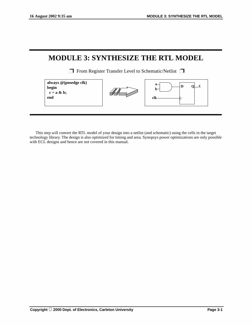
This step will convert the RTL model of your design into a netlist (and schematic) using the cells in the targettechnology library. The design is also optimized for timing and area. Synopsys power optimizations are only possiblewith ECL designs and hence are not covered in this manual.
MODULE 3: SYNTHESIZE THE RTL MODEL
From Register Transfer Level to Schematic/Netlist
always @(posedge clk)begin c = a & b;end
ab
clk
D Q c
Copyright 2000 Dept. of Electronics, Carleton University Page 3-1
16 August 2002 9:35 am MODULE 3: SYNTHESIZE THE RTL MODEL
This chapter describes using a Synopsys tool to compile your Verilog description of hardware to a gate-levelnetlist. You can guide Synopsys by using either the menu-driven interface called the Design Analyzer, or by typing aseries of commands at the command line prompt. The typed commands are interactively executed by a programcalled “dc_shell” (for Design Compiler Shell). The menu approach is good for exploring the command options, sincethey appear as buttons/widgets in the popup windows, whereas the Design Compiler shell approach is more like agoing through a series of typed calculations in matlab. For all practical purposes, Design Compiler is running regard-less of whether you invoke Design Compiler or Design Analyzer. Design Analyzer just translates your menu/GUIdriven choices into Design Compiler commands for execution.
Menus and Script Files
The buttons and popup menus of the Design Analyzer are helpful in the beginning but you should quickly changeto using typed commands from a script file. It is much quicker since you will be running the same steps many times inthe process of fine tuning the constraints for your compilation. Even if you’re using the Design Analyzer GUI, youcan still directly issue Design Compiler commands by popping up a command line window(Setup->Command_Window). The command prompt says “design analyzer>” but it is really just the Design Com-piler interpreter dc_shell. You can have the dc-shell execute entire script files of commands by using the “include”command (type “help include” at the prompt).
You can also use scripts to replay entire Design Analyzer sessions. This is because all commands issued via theGUI menus/buttons will be stored in a log file as script commands. The file is called “command.log” if the dc_shellwas started up via Design Analyzer’s Command Window (as opposed to starting dc_shell from the UNIX prompt).You can edit this script file to keep only commands that you want. So you need only go through a lengthy sequence ofsearching for buttons once, after which you can repeat the entire sequence by invoking the script. However, “com-mand.log” gets overwritten every time Design Analyzer is started up, so save it to another name often e.g. choose afile name that includes the date and time. Similarly, “view_command.log”, which records the output of your session(including analyses reports) is overwritten each session. You will want to save these text results with a time stampalso.
You will notice that “command.log” has a very length beginning section full of initialization commands. Thisheader is often much longer than the sequence of commands for your Design Analyzer session. Since Design Ana-lyzer and Design Compiler always execute those initialization commands when they start up, you can delete themfrom the script.
Getting Help
• Use “help” command at dc_shell prompt.
• There is an on-line help menu button in the upper right corner of the Design Analyzer GUI window.
• The same pdf documents can be invoked from Unix using the synview command.
Redoing Synthesis Steps
Most synthesis settings apply to a module. If you apply some questionable settings that are not reversible, youwill want to go back to the most recently saved version of the design prior to the application of those settings.
We recommend that you go to HDLs subdirectory and try to get a closer look at the Fun Counter code. While goingthrough the code, you should be able to identify how many flip-flops, I/O pads, .. etc this code is going to infer.(Check your Verilog notes for more information on how flip-flops and/or latches get inferred). This is a good practicewhereby you foresee how the code is going to be synthesized and converted to cells. Then, later on, while you aresynthesizing the Verilog code, hopefully you will be able to compare what you expected to what actually getssynthesized. If your code is inferring any undesired cells, this might eventually lead to a malfunctioning or a slowerchip.
3.1 Background Information
Copyright 2000 Dept. of Electronics, Carleton University Page 3-2
16 August 2002 9:35 am MODULE 3: SYNTHESIZE THE RTL MODEL
Synopsys Design Analyzer provides a graphical (menu-driven and command-line) interface to the Synopsys toolsyou will be using during synthesis (HDL Compiler, Design Compiler, Test Compiler, Design Time).
3.2 Starting Synopsys Design Analyzer
• You must create a Work directory in the Synopsysdirectory if it doesn’t exist:
mkdir Work
• To start the Design Analyzer, type the following atthe Unix prompt (The & starts the Design Analyzer inbackground so that you can use the Unix window forother commands):
design_analyzer &↵• Optionally, you can use the Design Compiler (dc)
shell and run the synthesis using dc shell commandsonly. Since the dc shell is a text-based window, youwill not be able to see the schematic. It is thereforenot advisable to use the dc shell alone until you arevery experienced.
You will be able to run a combination of script com-mands and menu commands by using the commandwindow inside the design anaylzer.
To start the dc shell, type the following at the Unixprompt:
Always start the design_analyserin the directory with .synopsys_dc.setup
Your Verilogor VHDLfiles
You create a Work directory, where the compiled
default library and is called WORK.
versions of your files will be stored. Thecontents of this directory is known as your
Errors, Warnings, & Reports
Copyright 2000 Dept. of Electronics, Carleton University Page 3-3
16 August 2002 9:35 am MODULE 3: SYNTHESIZE THE RTL MODEL
Design Compiler (dc) shell commands can be executed using the Design Analyzer command window. DesignCompiler commands are usually easier to execute than their Design Analyzer menu equivalents. They can also be col-lected up in a file to be executed as a script in either the dc shell or the Design Analyzer command window.
The command window is also used as a report window for all commands executed in the Design Analyzer. There-fore, after executing a command (using either the command window or the Design Analayzer menus), you mustalways check the results the report generated in the command window. It is easier to debug and correct errors at anearlier stage of synthesis.
Copyright 2000 Dept. of Electronics, Carleton University Page 3-4
16 August 2002 9:35 am MODULE 3: SYNTHESIZE THE RTL MODEL
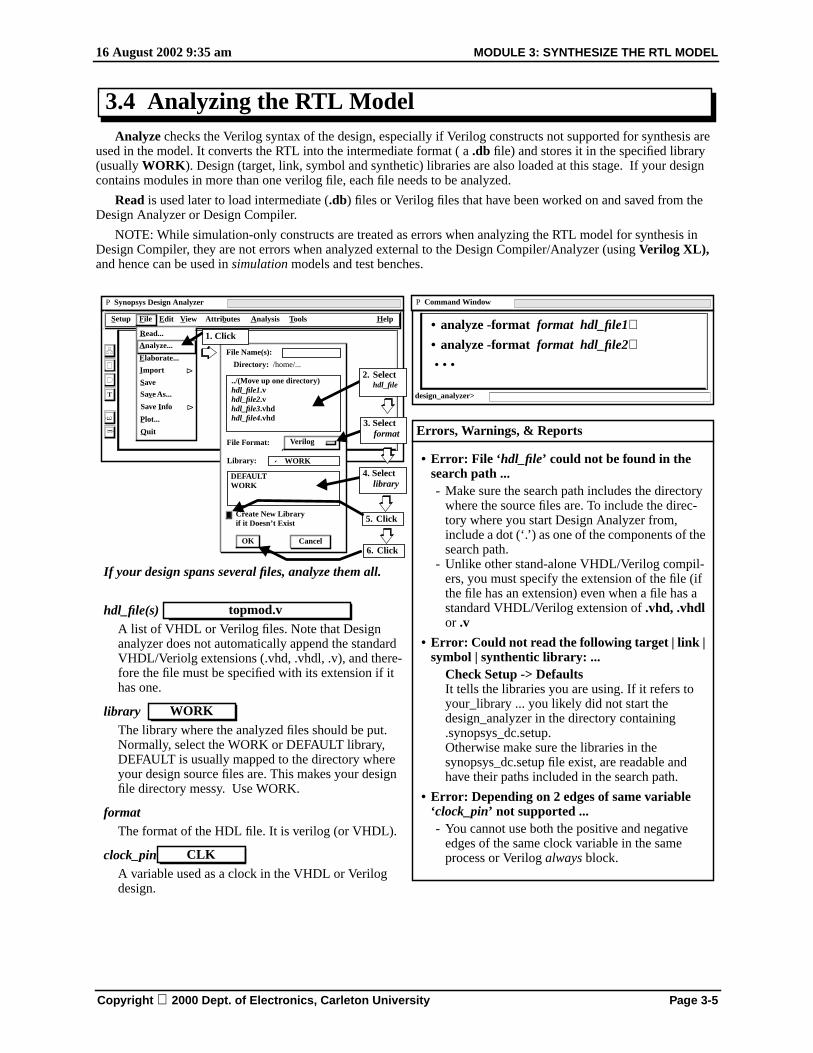
Analyze checks the Verilog syntax of the design, especially if Verilog constructs not supported for synthesis areused in the model. It converts the RTL into the intermediate format ( a .db file) and stores it in the specified library(usually WORK). Design (target, link, symbol and synthetic) libraries are also loaded at this stage. If your designcontains modules in more than one verilog file, each file needs to be analyzed.
Read is used later to load intermediate (.db) files or Verilog files that have been worked on and saved from theDesign Analyzer or Design Compiler.
NOTE: While simulation-only constructs are treated as errors when analyzing the RTL model for synthesis inDesign Compiler, they are not errors when analyzed external to the Design Compiler/Analyzer (using Verilog XL),and hence can be used in simulation models and test benches.
3.4 Analyzing the RTL Model
• Error: File ‘hdl_file’ could not be found in thesearch path ...- Make sure the search path includes the directory
where the source files are. To include the direc-tory where you start Design Analyzer from,include a dot (‘.’) as one of the components of thesearch path.
- Unlike other stand-alone VHDL/Verilog compil-ers, you must specify the extension of the file (ifthe file has an extension) even when a file has astandard VHDL/Verilog extension of .vhd, .vhdlor .v
• Error: Could not read the following target | link |symbol | synthentic library: ...
Check Setup -> DefaultsIt tells the libraries you are using. If it refers toyour_library ... you likely did not start thedesign_analyzer in the directory containing.synopsys_dc.setup.Otherwise make sure the libraries in thesynopsys_dc.setup file exist, are readable andhave their paths included in the search path.
• Error: Depending on 2 edges of same variable‘clock_pin’ not supported ...- You cannot use both the positive and negative
edges of the same clock variable in the sameprocess or Verilog always block.
P Synopsys Design Analyzer
È
È
T
P Command Window
• analyze -format format hdl_file1↵• analyze -format format hdl_file2↵ • • •
design_analyzer>
If your design spans several files, analyze them all.
hdl_file(s)A list of VHDL or Verilog files. Note that Designanalyzer does not automatically append the standardVHDL/Veriolg extensions (.vhd, .vhdl, .v), and there-fore the file must be specified with its extension if ithas one.
libraryThe library where the analyzed files should be put.Normally, select the WORK or DEFAULT library,DEFAULT is usually mapped to the directory whereyour design source files are. This makes your designfile directory messy. Use WORK.
formatThe format of the HDL file. It is verilog (or VHDL).
clock_pinA variable used as a clock in the VHDL or Verilogdesign.
topmod.v
WORK
CLK
Errors, Warnings, & Reports
File Name(s):
Directory: /home/...
Create New Libraryif it Doesn’t Exist
File Format:
../(Move up one directory)hdl_file1.vhdl_file2.vhdl_file3.vhdhdl_file4.vhd
16 August 2002 9:35 am MODULE 3: SYNTHESIZE THE RTL MODEL
Elaborating builds the design from the intermediate format of the “analyze” step. The RTL model is convertedinto generic gates and logic blocks. Again, constructs not supported for synthesis (such as using both clock edges in aprocess or always block) are reported. The elaborate process also reports the memory elements (flip-flops and latches)and tristate-buffers implied in your design. Since elaboration works through all the modules of a design hierarchy,only the top-most module needs to be elaborated. After elaboration, the Design Analyzer window should showone icon for each module in your design.
3.5 “Elaborating” the Design
• Error: Clock variable ‘clock_pin’ is being used asdata in ...- clock_pin, used as a clock with the statements
like clock_pin’event and clock_pin = ‘1’ (= ‘0’)or posedge (negedge) clock_pin, cannot be usedin the right-hand side of an assignment statementin the same process or always block. Use a sepa-rate process or always block to make this assign-ment.
• Error: This use of clock edge specification notsupported in ...- You cannot use both the positive and negative
clock edges of the same clock variable in thesame process or always block.
- In VHDL, you cannot use more than oneclock_pin’event and clock_pin = ‘1’ (= ‘0’) clockstatements in one process. If possible, make allassignments in one clock statement or use morethan one process.
• Info: Inferred memory devices in process ...
• Info: Inferred THREE-STATE control devices inprocess ...- Always check this information about inferred
devices to make sure that your RTL descriptiondoes not imply unnecessary flip-flops (due to var-iable assignments in clock_pin’event andclock_pin = ‘1’ (= ‘0’) statements or alwaysblocks with posedge (negedge) clock_pin state-ments), latches (due to variables not assigned toin all conditions of if and case statements - toavoid latches, also make the variable assignmentin the else or default clauses of these statements),and tristate buffers.
P Synopsys Design Analyzer
È
È
T
P Command Window
• elaborate module↵ // for Verilog
• (elaborate entity↵) // for VHDL
design_analyzer>
entityThe entity name of the topmost VHDL model. Thiswill find and elaborate lower level modules providedthey have been analyzed.
archThe architecture of the VDHL entity.
moduleThe module name of the top Verilog model. This willfind and elaborate lower level modules provided theyhave been analyzed.
libraryThe library where the files were analyzed into. Nor-mally, select the WORK or DEFAULT library,which is usually mapped to the directory where yourdesign source files are.
clock_pinA variable used as a clock in the VHDL or Verilogmodel.
00 Dept. of Electronics, Carl eton University Page 3-6
16 August 2002 9:35 am MODULE 3: SYNTHESIZE THE RTL MODEL
This checks the Current Design for problems. All errors must be corrected. While most warnings can be ignored,it is necessary to check each one of them since some warnings might actually indicate errors in the logic of the design.Click on the top module and ensure it is shown as “the design” at the bottom of the Design Analyzer window. Thendo the following:
3.6 Check the Design Rules
• Warning: In design ‘design’ port ‘port_name’ isnot connected to any nets.
Make sure that the port port_name is intention-ally not associated with any logic in your HDLdescription e.g. for scan test pins. For example, ifthe port is included for future expansion of thedesign, or for component interface consistency,the warning may be ignored.
• Warning: In design ‘design’ net ‘net_name’ has aconnection class violation.
This message will show up for wires connectingcore logic circuitry to I/O pads. It can beignored.
P Synopsys Design Analyzer
È
È
T
P Command Window
• check_design↵
design_analyzer>
designThe name of the design you are currently checking.
Copyright 2000 Dept. of Electronics, Carleton University Page 3-7
16 August 2002 9:35 am MODULE 3: SYNTHESIZE THE RTL MODEL
You may now save the design in the Synopsys internal database (.db) format. This is important if you wish to stopat this stage and continue the design process later. The saved db file will allow you to read in the current state of thedesign without having to analyze the files, re-elaborate, and check_design again from the RTL model.
The save command outlined here will save all the designs in the hierarchy in a file named file_name.. Usuallyfile_name is made the name of the top-level module (Verilog) and should end with suffix .db. In this case, the topmodule is the I/O pad wrapper, so first click on that module and ensure that it is shown to be “the design” at the bot-tom of the Design Analyzer window.
file_nameThe file name where you save the optimized versionofyour design.
file_formatSave in Synopses’ internal format..
db
Copyright 2000 Dept. of Electronics, Carleton University Page 3-8
16 August 2002 9:35 am MODULE 3: SYNTHESIZE THE RTL MODEL
Design Compiler maps the overall design to gates according to a set of criteria known as constraints. Design con-straints are necessary conditions that have to be met for the circuit to function properly, whereas optimization con-straints are things that the designer consider “nice”, cheap, profitable, small, etc.. Many design constraints arerelated to the signal timing and electrical loading that the cell libraries are designed for, while optimization con-straints are driven by the circuit application and operating context. Design constraints are given priority over optimi-zation constraints (otherwise the circuit won’t work even if it is small/fast/power-efficient etc.).
Design Hierarchy, Core Circuitry, and I/O Pad Module
Constraints must be set prior to compiling (mapping/optimization) the design. In order to apply constraints,Design Compiler maintains the notion of a design hierarchy, where each design in the hierarchy corresponds to a Ver-ilog module. Generally speaking, Design Compiler applies constraints to the currently selected design, which isshown as “the design” at the bottom of the Design Analyzer window. Constraints are typically applied to the top mod-ule and propagated down to lower level modules as a separate step. However, in this tutorial, the top-most synthesiz-able module is just a wrapper consisting of a technology-specific set of I/O buffer pads connected to a technology-independent core circuit. Since the core contains all the logic function, some constraints will only make senseapplied to the core’s “top” rather than the very top wrapper module (most notably, constraints related to design forfunctional scan testing). All constraints will be propagated to lower level design modules as a separate step, regard-less of whether they were applied to the core or the top-most wrapper.
Motivations and Cautions of the I/O Pad Wrapper Layer
There are trade-offs associated with using a wrapper layer to specify the I/O pads right from the start at the RTLstage. One of the reasons for choosing this approach is that Design Compiler’s pad insertion can choose inappropri-ate pads based on the requirements. Therefore, the designer should choose pads based on understanding of the condi-tion of the incoming signals and the load for outgoing signals. Furthermore, the I/O floorplan should be determinedprior to synthesis, based on outer-world restrictions such as bonding capabilities or requirements in connecting withother circuits. Therefore, the pads and the pad frame floorplan need to be selected ahead of time based on the top-down applications and restrictions (electrical loading, speed, test equipment) as well as the bottom-up capabilities ofthe pads available for the target technology library. This complicates the life of the designer, because the generic ver-ilog design that use to depend only on logic functionality must now have technology dependent pads. Since fabrica-tion technology changes every year, we try to minimize the interdependence of the technology dependent pads withthe core logic by putting all the pads into a wrapper layer of structural verilog.
Preplanning a pad wrapper layer has further benefits. All the I/O pads are that the pads are collected in one mod-ule. If you leave it upto Design Compiler, the pads could be placed anywhere in the design hierarchy. You alsochoose meaningful names for the pads so that you can actually recognize them during place and route.
Making the Pads “Off-Limits” to Modification/Optimization
Since the pads in the RTL wrapper are instantiations of actual library cells to be inserted, Design Compiler mustbe told not to modify them in trying to meet its constraints. The following command should now be typed into theentry part of the command window (the single line at the bottom):
set_dont_touch find( cell { "*_ip" , "*_op" } )
This assumes that the input and output pads have instantiation names ending in “_ip” and “_op”, and that no othercells have this. Otherwise, the cell specification for the don’t-touch command may have to be more specific, possiblyspecifying each pad instance individually. Check the command window log after this command to verify the affectedcells. Any wrongly affected cells can be corrected by the command
remove_attribute find(cell “name”) dont_touch
3.8 Setting Constraints for Synthesis
Copyright 2000 Dept. of Electronics, Carleton University Page 3-9
16 August 2002 9:35 am MODULE 3: SYNTHESIZE THE RTL MODEL
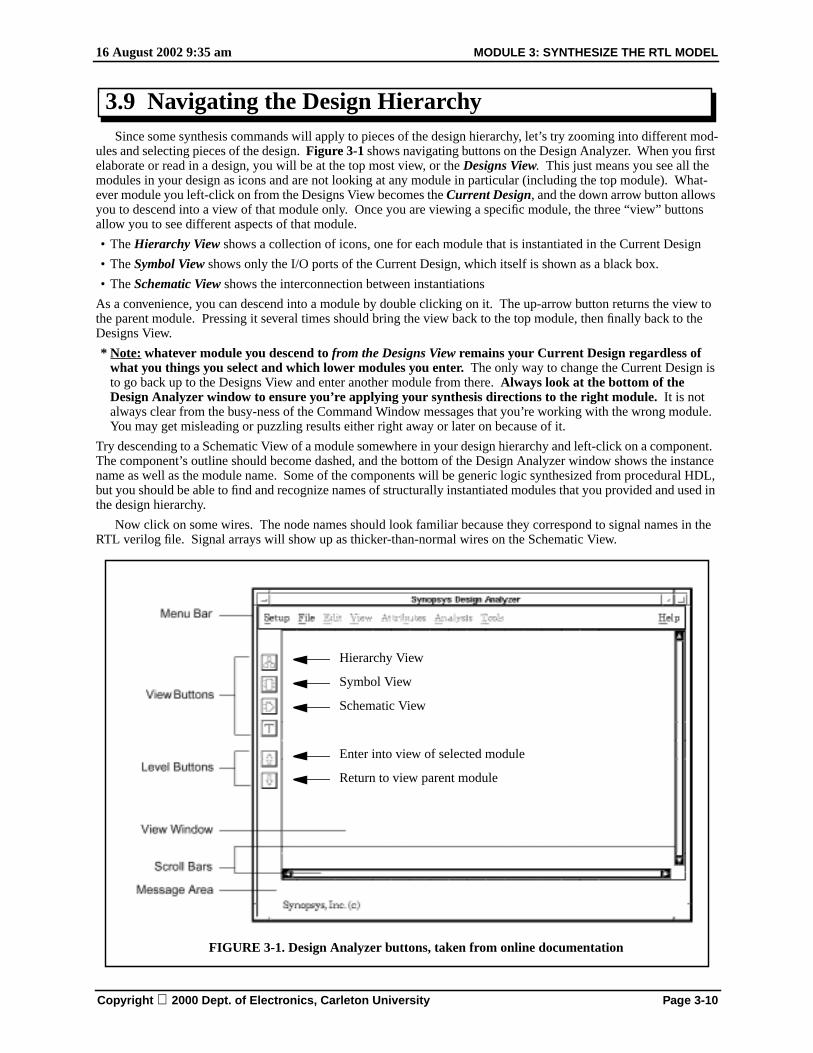
Since some synthesis commands will apply to pieces of the design hierarchy, let’s try zooming into different mod-ules and selecting pieces of the design. Figure 3-1 shows navigating buttons on the Design Analyzer. When you firstelaborate or read in a design, you will be at the top most view, or the Designs View. This just means you see all themodules in your design as icons and are not looking at any module in particular (including the top module). What-ever module you left-click on from the Designs View becomes the Current Design, and the down arrow button allowsyou to descend into a view of that module only. Once you are viewing a specific module, the three “view” buttonsallow you to see different aspects of that module.
• The Hierarchy View shows a collection of icons, one for each module that is instantiated in the Current Design
• The Symbol View shows only the I/O ports of the Current Design, which itself is shown as a black box.
• The Schematic View shows the interconnection between instantiations
As a convenience, you can descend into a module by double clicking on it. The up-arrow button returns the view tothe parent module. Pressing it several times should bring the view back to the top module, then finally back to theDesigns View.
* Note: whatever module you descend to from the Designs View remains your Current Design regardless ofwhat you things you select and which lower modules you enter. The only way to change the Current Design isto go back up to the Designs View and enter another module from there. Always look at the bottom of theDesign Analyzer window to ensure you’re applying your synthesis directions to the right module. It is notalways clear from the busy-ness of the Command Window messages that you’re working with the wrong module.You may get misleading or puzzling results either right away or later on because of it.
Try descending to a Schematic View of a module somewhere in your design hierarchy and left-click on a component.The component’s outline should become dashed, and the bottom of the Design Analyzer window shows the instancename as well as the module name. Some of the components will be generic logic synthesized from procedural HDL,but you should be able to find and recognize names of structurally instantiated modules that you provided and used inthe design hierarchy.
Now click on some wires. The node names should look familiar because they correspond to signal names in theRTL verilog file. Signal arrays will show up as thicker-than-normal wires on the Schematic View.
3.9 Navigating the Design Hierarchy
FIGURE 3-1. Design Analyzer buttons, taken from online documentation
Hierarchy View
Symbol View
Schematic View
Enter into view of selected module
Return to view parent module
Copyright 2000 Dept. of Electronics, Carleton University Page 3-10
16 August 2002 9:35 am MODULE 3: SYNTHESIZE THE RTL MODEL
Next, try selecting ports (module parameters, or “I/O” for that module). These should be visible from the Sche-matic and Symbol Views. Ports for arrays should be drawn with thicker lines. You should recognize the names thatare shown. In the top-most wrapper module and the top-most module of the core, you should see the unconnectedpins for scan testing I/O (if you left any for this purpose...it isn’t always necessary, since scan I/O pins can often bemultiplexed with regular I/O pins).
Handy Mouse Actions
• Select a whole bunch of things inside of any rectangular region of your choosing by holding down the left mouse,dragging out a rectangle, and letting go.
• Zoom in by holding down the right mouse button, pointing at Zoom, and letting go.
• Zoom out for a full view the same way, but pointing at Full View instead.
Copyright 2000 Dept. of Electronics, Carleton University Page 3-11
16 August 2002 9:35 am MODULE 3: SYNTHESIZE THE RTL MODEL
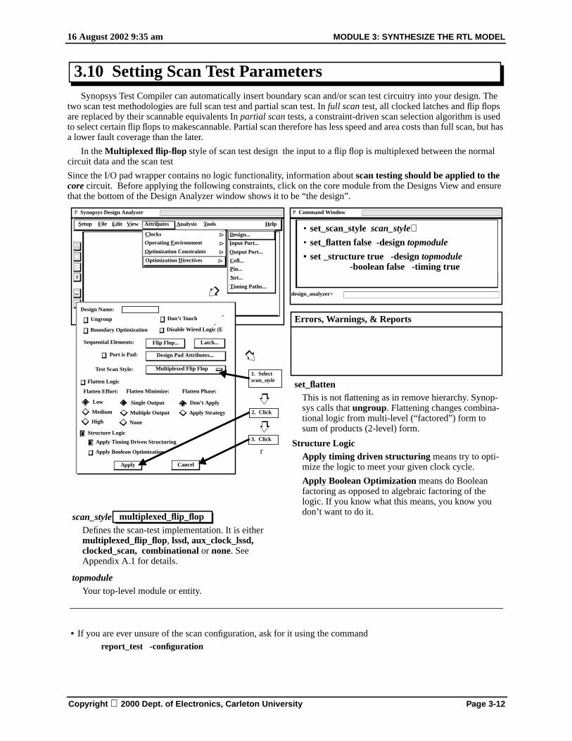
Synopsys Test Compiler can automatically insert boundary scan and/or scan test circuitry into your design. Thetwo scan test methodologies are full scan test and partial scan test. In full scan test, all clocked latches and flip flopsare replaced by their scannable equivalents In partial scan tests, a constraint-driven scan selection algorithm is usedto select certain flip flops to makescannable. Partial scan therefore has less speed and area costs than full scan, but hasa lower fault coverage than the later.
In the Multiplexed flip-flop style of scan test design the input to a flip flop is multiplexed between the normalcircuit data and the scan test
Since the I/O pad wrapper contains no logic functionality, information about scan testing should be applied to thecore circuit. Before applying the following constraints, click on the core module from the Designs View and ensurethat the bottom of the Design Analyzer window shows it to be “the design”.
• If you are ever unsure of the scan configuration, ask for it using the commandreport_test -configuration
• set _structure true -design topmodule -boolean false -timing true
design_analyzer>
scan_styleDefines the scan-test implementation. It is eithermultiplexed_flip_flop, lssd, aux_clock_lssd,clocked_scan, combinational or none. SeeAppendix A.1 for details.
set_flattenThis is not flattening as in remove hierarchy. Synop-sys calls that ungroup. Flattening changes combina-tional logic from multi-level (“factored”) form tosum of products (2-level) form.
Structure LogicApply timing driven structuring means try to opti-mize the logic to meet your given clock cycle.
Apply Boolean Optimization means do Booleanfactoring as opposed to algebraic factoring of thelogic. If you know what this means, you know youdon’t want to do it.
Copyright 2000 Dept. of Electronics, Carleton University Page 3-12
16 August 2002 9:35 am MODULE 3: SYNTHESIZE THE RTL MODEL
If you don’t designate pins for scan in or out, Design Compiler will multiplex those signals with regular pins of itschoosing. If you have any ports and pads intended either solely for scan I/O, or meant to be multiplexed with scan I/O, you should now designate them for that purpose. First, descend into a Symbol View of the top core module.
For Scan Out
• Select the desired output port, then go to the menu item:Attributes -> Optimization Directives -> Output Port...
• In the Output Port Attributes form change Signal Type to Scan Out
• Click Apply and Cancel.
For Scan Enable
This pin is probably better to choose yourself. If left to Design Compiler, it also takes the liberty of sometimes mak-ing it active-low, which can mess up your test results unless you actively look for it.
• Double-click on the desired input port and the Input Port Attributes form should come up. Select:Signal Type: Test -> Scan Enable
• Click Apply
For Scan In
• Repeat for the desired scan in input pin, changing its Signal Type to Test -> Scan In
Always click Apply after changing a form.
Design Compiler now knows which pins to use for scan-based test.
You can Cancel the open forms.
Return to the top-level module of this design for the remainder of the constraints.
To do this, click the Up-Arrow until you get back up to the top-most Design View, then double click on the top mod-ule (the pad wrapper module).
• Click on the Symbol view button (from the left-side of the Synopsys Design Analyzer window) if you are notalready viewing the Symbol View of the top I/O-pad wrapper module.
• To set the expected output load, select the all output ports (draw a box around them, or click on one, then hold shiftwhile you click on the other) and select: Attributes -> Operating Environment -> Load...
• Enter a Capacitive load: of 20The units for capacitance in this library are picofarads.
• Click Apply then Cancel
3.11 Designating Pins for Scan Test I/O
3.12 Define the output load
Copyright 2000 Dept. of Electronics, Carleton University Page 3-13
16 August 2002 9:35 am MODULE 3: SYNTHESIZE THE RTL MODEL
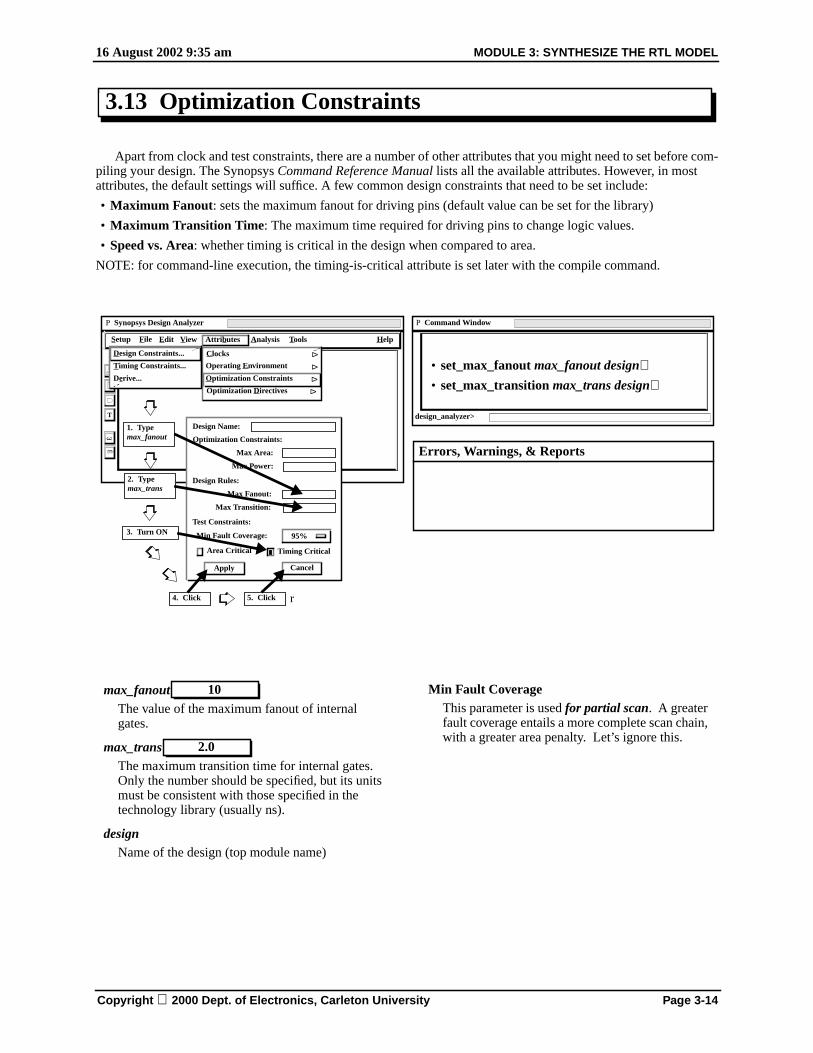
Apart from clock and test constraints, there are a number of other attributes that you might need to set before com-piling your design. The Synopsys Command Reference Manual lists all the available attributes. However, in mostattributes, the default settings will suffice. A few common design constraints that need to be set include:
• Maximum Fanout: sets the maximum fanout for driving pins (default value can be set for the library)
• Maximum Transition Time: The maximum time required for driving pins to change logic values.
• Speed vs. Area: whether timing is critical in the design when compared to area.
NOTE: for command-line execution, the timing-is-critical attribute is set later with the compile command.
max_fanoutThe value of the maximum fanout of internalgates.
max_transThe maximum transition time for internal gates.Only the number should be specified, but its unitsmust be consistent with those specified in thetechnology library (usually ns).
Min Fault CoverageThis parameter is used for partial scan. A greaterfault coverage entails a more complete scan chain,with a greater area penalty. Let’s ignore this.
Copyright 2000 Dept. of Electronics, Carleton University Page 3-14
16 August 2002 9:35 am MODULE 3: SYNTHESIZE THE RTL MODEL
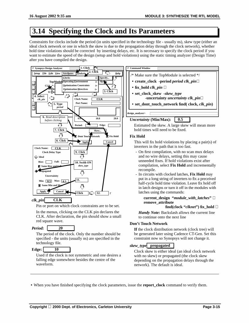
Constraints for clocks include the period (in units specified in the technology file - usually ns), skew type (either anideal clock network or one in which the skew is due to the propagation delay through the clock network), whetherhold time violations should be corrected by inserting delays, etc. It is necessary to specify the clock period if youwant to estimate the speed of the design (setup and hold violations) using the static timing analyzer (Design Time)after you have compiled the design.
• When you have finished specifying the clock parameters, issue the report_clock command to verify them.
3.14 Specifying the Clock and Its Parameters
P Synopsys Design Analyzer
È
È
T
P Command Window
/* Make sure the TopModule is selected */
• create_clock -period period clk_pin↵• fix_hold clk_pin ↵• set_clock_skew -skew_type
Uncertainty (Min/Max):Estimated the skew. A large skew will mean morehold times will need to be fixed.
Fix HoldThis will fix hold violations by placing a pair(s) ofinverters in the path that is too fast.- On first compilation, with no scan mux delays
and no wire delays, setting this may causeunneeded fixes. If hold violations exist aftercompilation, select Fix Hold and incrementallyrecompile.
- In circuits with clocked latches, Fix Hold mayput in a long string of inverters to fix a preceivedhalf-cycle hold time violation. Leave fix hold offin latch designs or turn it off in the modules withlatches using the commands:
find(clock “clknet”) fix_hold ↵Handy Note: Backslash allows the current lineto continue onto the next line
Don’t Touch NetworkIf the clock distribution network (clock tree) willbe generated later using Cadence CT-Gen. Set thisconstraint now so Synopsys will not change it.
skew_typeClock skew is either ideal (an ideal clock networkwith no skew) or propagated (the clock skewdepending on the propagation delays through thenetwork). The default is ideal.
0.5
propagated
9. Click
CLK
0.5
TopModule
CLK
0.5
Copyright 2000 Dept. of Electronics, Carleton Univers
ity Page 3-15
16 August 2002 9:35 am MODULE 3: SYNTHESIZE THE RTL MODEL
3.15 Annotating activity for Power analysis
Within Synopsys there is a power analysis tool which will let us estimate power consumption under varioucon-ditions and configurations. In order to get realistic estimates however, we need to tell the tool how often variousnodes will be toggling.
We use the annotate_activity command from the command window. For help, you can type manannotate_activity. The commands to be run, from the _chip level of the hierarchy are:
annotate_activity -hier -select all -static_probability 0 -clock clk -objects {reset,test_se,test_si,loadenable}
annotate_activity -hier -select all -static_probability 1 -clock clk -objects {countenable}
annotate_activity -hier -select all -clock clk -toggle_rate 0.5 -objects {FCc/SeqPart/state_0_}
annotate_activity -hier -select all -clock clk -toggle_rate 0.25 -objects {FCc/SeqPart/state_1_}
annotate_activity -hier -select all -clock clk -toggle_rate 0.125 -objects {FCc/SeqPart/state_2_}
The static_probability is the P[signal=1]. We set some of the values as constant so that they don’t effect ourpower measurements. For the actual counter, it is important to annotate the switching activities of the outputs.Although it isn’t sequential, it is a counter and so we know that they toggle at a rate of 0.125-MSB, 0.25 , 0.5LSB on average. To specify the signal names can be quite a chore. Often we would use the find command.
Now that we have annotated the switching activities, after compilation, we can get reasonable power-estimateswith the "report_power" command. We could also specify power as an optimization constraint, so that thecompiler tries to minimize power over such things as area and delay.
Copyright 2000 Dept. of Electronics, Carleton University Page 3-16
16 August 2002 9:35 am MODULE 3: SYNTHESIZE THE RTL MODEL
A number of problems in the compilation are avoided by the set_fix_multiple_port_nets command, whichinserts logic to ensure that there are no feedthroughs, or any driving of multiple port by a single net.
You should also propagate all the constraints on the top module to the lower level modules. Again this is donefrom the command line prompt using characterize.
• After fixing the ports and propagating constraints, save the constrained design as a db file from the top module.Use a descriptive new name like TopModule_constrained.db (don’t clobber the version you saved before). Thismakes it easy to come back to this point if you change the design in unintended ways.
3.16 Propagating Constraints Throughout the Hierarchy
P Synopsys Design Analyzer
È
È
T
P Command Window
• set_fix_multiple_port_nets -all↵• characterize -constraints other modinst↵
/* To save in the command window use */
write -format db -hierarchy -output topmod_constrained.db topmod↵
design_analyzer>
other_modinst
Lower level module instances to which the constraintsshould be propagated (basically, all of them). Aftercharacterization you should see the red square wave onthe clock pin of the lower level module.• More than one instance should be in a list, as illus-
File_nameWe suggest you save your design with thesufix constrained.db. This allows the file to beeasily found and loaded for restarting from thispoint.
File_formatThe db format is Synopses’ own internal fileformat. Use it if the file is not used outsideSynopsys.
topmod_constrained.db
db
Copyright 2000 Dept. of Electronics, Carleton University
Page 3-17
16 August 2002 9:35 am MODULE 3: SYNTHESIZE THE RTL MODEL
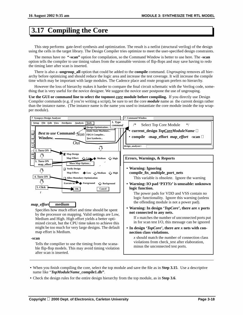
This step performs gate-level synthesis and optimization. The result is a netlist (structural verilog) of the designusing the cells in the target library. The Design Compiler tries optimize to meet the user-specified design constraints.
The menus have no “-scan” option for compilation, so the Command Window is better to use here. The -scanoption tells the compiler to use timing values from the scannable versions of flip-flops and may save having to redothe timing later after scan is inserted.
There is also a -ungroup_all option that could be added to the compile command. Ungrouping removes all hier-archy before optimizing and should reduce the logic area and increase the test coverage. It will increase the compiletime which may be important with large modules. The Cadence place and route program prefers no hierarchy.
However the loss of hierarchy makes it harder to compare the final circuit schematic with the Verilog code, some-thing that is very useful for the novice designer. We suggest the novice user postpone the use of ungrouping.
Use the GUI or command line to select the topmost core module before compiling. If you directly use DesignCompiler commands (e.g. if you’re writing a script), be sure to set the core module name as the current design ratherthan the instance name. (The instance name is the name you used to instantiate the core module inside the top wrap-per module).
• When you finish compiling the core, select the top module and save the file as in Step 3.15. Use a descriptivename like “TopModuleName_compile1.db”.
• Check the design rules for the entire design hierarchy from the top module, as in Step 3.6.
map_effortSpecifies how much effort and time should be spentby the processor on mapping. Valid settings are Low,Medium and High. High effort yields a better opti-mized circuit, but the CPU time taken to achieve thismight be too much for very large designs. The defaultmap effort is Medium.
-scanTells the compilier to use the timing from the scana-ble flip-flop models. This may avoid timing violationafter scan is inserted.
medium
• Warning: Ignoringcompile_fix_multiple_port_nets
This variable is obsolete. Ignore the warning
• Warning: IO pad ‘PXYYz’ is unusable: unknownlogic function.
The power pads for VDD and VSS contain nologic functionality. Ignore this warning (unlessthe offending module is not a power pad).
• Warning: In design ‘TopCore’, there are x portsnot connected to any nets.
If x matches the number of unconnected ports putin for scan test I/O, this message can be ignored
• In design ‘TopCore’, there are x nets with con-nection class violations.
x should match the number of connection classviolations from check_test after elaboration,minus the unconnected test ports.
16 August 2002 9:35 am MODULE 3: SYNTHESIZE THE RTL MODEL
By having Design Compiler generate several analysis reports, the results of the core compilation can be checkedto see if any constraints are violated, where they were violated, and how much area it costed. If there are violations(especially related to timing), you can run an incremental compilation on the core, which starts with the existinggate-level design and proceeds to atempt further optimization. Since we will be running an incremental compilationto incorporate the wrapper, let’s not worry too much about the incremental core compilation.
Select the top wrapper module to perform the following analyses.
• The report_constraints command is not always clear about where a violation takes place (which signal path ornode). The -verbose option for this command should give the details.
• Minor timing violations seem to go unreported, presumably because the analysis is approximate. Furthermore, theplace-and-route tool gives priority to eliminating violations, so minor violations at this stage are not likely toremain a problem.
• Because the clock line is routed everywhere and feeds many cells, it will have a large capacitance. It may violatethe maximum transition time and fanout. This is OK because the single clock node will actually be implementedas a buffered clock tree in the physical design stage. The timing slack of critical paths should not be affectedbecause they depend on the clock period.
• report_power command can be done here or you may wish to select from the form.
3.18 Analyzing Area, Timing, and Constraint Violations
• Report: In the contraints report, note the (MET)and (VIOLATED) against each of the design con-straints set earlier.- This shows that the design constraint has either
been met or violated by the indicated value.
• Report: In the timing report, note the slack (MET)at the end of the report. - This indicates the time that the longest path in the
design settles before the clock changes. A nega-tive value indicates a violation. Increase theclock period or reoptimize the design if there is aslack violation.
Copyright 2000 Dept. of Electronics, Carleton University Page 3-19
16 August 2002 9:35 am MODULE 3: SYNTHESIZE THE RTL MODEL
The core module now has been synthesized into CMOSP35-specific gates. The top wrapper module should nothave been changed by the compile. Figure 3-2 shows the schematic view of top wrapper module. None of the syn-thesis steps in the design flow should modify this module.
As a designer you should have a much better idea now about your final design size, and if you will be able to meetyour timing goal or not. Keep in mind that the timing values used are based on wireload files and may still be quitedifferent from post-layout values.
An incremental compile will be performed on this design.
• Select the top wrapper module from the Designs View.
• Attempt an incremental compile with high effort as follows:design_analyzer> compile -scan -map_effort high -incremental_map
• Save the overall design as a db file from the top wrapper module with a descriptive new name likeTopModuleName_compile2.db
• Repeat the Check Design and Report steps.
For the purpose of this tutorial, you can continue if you have no violations, or if your timing violation is less than2 ns. For your own designs, experience will tell you how much of a violation can be overcome by the placement androuting tools. If timing is not close, the design structure or performance goals may need to be rethought.
It is good practice to visually inspect the I/O wrapper module to ensure it still contains all the I/O pads and noother logic cells.
3.19 Compile the Whole Design From the Top Wrapper
FIGURE 3-2. The top wrapper module should not have been changed by the core compilation.
I/O PAD
I/O PAD
COREMODULE
TOP LEVELWRAPPERMODULE
PIN
BUS
WIRE
Copyright 2000 Dept. of Electronics, Carleton University Page 3-20
16 August 2002 9:35 am MODULE 3: SYNTHESIZE THE RTL MODEL
The purpose of the next two steps is to get an idea of how successful scan-based test will be with this specific design.If the fault coverage is lower than required/expected, you may need to re-think the RTL code or you may have a cod-ing error in your design. If basic design methods are followed, fault coverage well above 90% should be obtained.
Here, we check the design against the design rules of the selected scan test methodology and scan style. This must bedone prior to inserting scan test circuitry and generating test patterns. Again, while it is not necessary to correct warn-ings, remembered that the causes of these warnings will usually reduce the fault coverage.
Since the top wrapper module only contains I/O pads, and in order to avoid some scan chain insertion problems, thescan chain will be inserted directly into the core module.
• Select the core module from the Designs View.
• In this step, make the scan_style on the GUI panel the same as in Step 3.10.
• Both the scan_style and the test_methodology can always be checked usingreport_test -configuration
3.20 Checking the Test Design Rules
P Synopsys Design Analyzer
È
È
T
P Command Window
• set_test_methodology test_methodology
• check_test↵
design_analyzer>
test_methodologyThe test methodology to be used. It is either full_scanor partial_scan. The default is full_scan.
scan_styleEnsure this is set the same as in Step 3.10.
full_scan
multiplexed_flip_flop
• Warning:warnings may be ignored but will usually reducetest coverage.
Copyright 2000 Dept. of Electronics, Carleton University Page 3-21
16 August 2002 9:35 am MODULE 3: SYNTHESIZE THE RTL MODEL
At this point, you can optionally estimate the test fault coverage. The higher your fault coverage, the fewer defec-tive chips will be packaged and placed in product. Reducing the number of defective chips used at the time of initialtesting (with the scan-based test) reduces the time and money spent on defective product.
Fault coverage is estimated by running automatic test pattern generation (ATPG) on the design. This is especiallyimportant if you had warnings when running check test design rules in Step 3.19. By running ATPG at this point, youget an idea of the effect that the warnings (usually uncontrollable pins) have on the fault coverage. You can thendecide whether to correct the warnings or not.
You should get a warning about not having a scan path, since that is to be inserted next. Test vectors will be gen-erated on the assumption that all valid scan FF’s will be included in the scan path. First random scan vectors are gen-erated, and the fault-coverage provided by those vectors is determined. Next, specific vectors are generated in anattempt to isolate faults which were not detected by random patterns. Finally, all the vectors are "collapsed" to pro-duce the minimum set of vectors required to test the maximum number of faults.
3.21 Estimating Test Fault Coverage
• Warning: Design has no scan path. Generatedvectors will not be saved.
Ignore this warning. It simply reminds you thatyou have run ATPG before inserting scan test cir-cuitry. ATPG will be run again later.
16 August 2002 9:35 am MODULE 3: SYNTHESIZE THE RTL MODEL
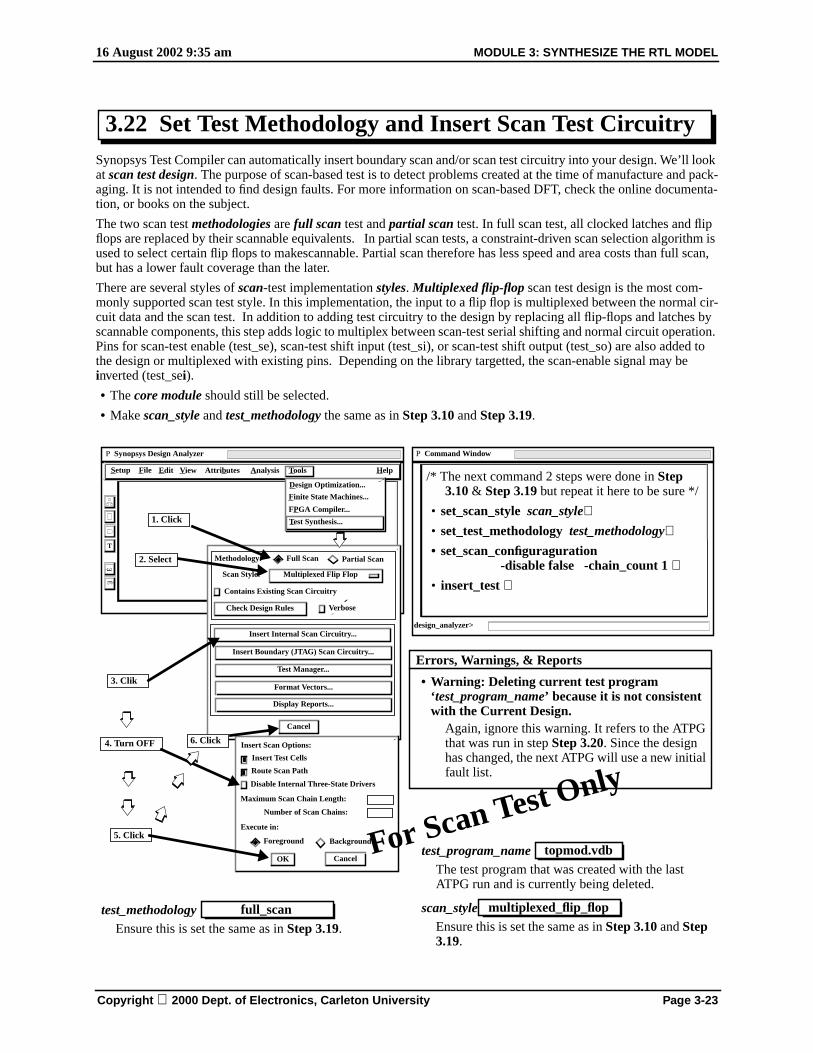
Synopsys Test Compiler can automatically insert boundary scan and/or scan test circuitry into your design. We’ll lookat scan test design. The purpose of scan-based test is to detect problems created at the time of manufacture and pack-aging. It is not intended to find design faults. For more information on scan-based DFT, check the online documenta-tion, or books on the subject.
The two scan test methodologies are full scan test and partial scan test. In full scan test, all clocked latches and flipflops are replaced by their scannable equivalents. In partial scan tests, a constraint-driven scan selection algorithm isused to select certain flip flops to makescannable. Partial scan therefore has less speed and area costs than full scan,but has a lower fault coverage than the later.
There are several styles of scan-test implementation styles. Multiplexed flip-flop scan test design is the most com-monly supported scan test style. In this implementation, the input to a flip flop is multiplexed between the normal cir-cuit data and the scan test. In addition to adding test circuitry to the design by replacing all flip-flops and latches byscannable components, this step adds logic to multiplex between scan-test serial shifting and normal circuit operation.Pins for scan-test enable (test_se), scan-test shift input (test_si), or scan-test shift output (test_so) are also added tothe design or multiplexed with existing pins. Depending on the library targetted, the scan-enable signal may beinverted (test_sei).
• The core module should still be selected.
• Make scan_style and test_methodology the same as in Step 3.10 and Step 3.19.
3.22 Set Test Methodology and Insert Scan Test Circuitry
• Warning: Deleting current test program‘test_program_name’ because it is not consistentwith the Current Design.
Again, ignore this warning. It refers to the ATPGthat was run in step Step 3.20. Since the designhas changed, the next ATPG will use a new initialfault list.
P Synopsys Design Analyzer
È
È
T
P Command Window
/* The next command 2 steps were done in Step3.10 & Step 3.19 but repeat it here to be sure */
test_program_nameThe test program that was created with the lastATPG run and is currently being deleted.
scan_styleEnsure this is set the same as in Step 3.10 and Step3.19.
topmod.vdb
multiplexed_flip_flop
Copyright 2000 Dept. of Electronics, Carleton Univers
ity Page 3-23
16 August 2002 9:35 am MODULE 3: SYNTHESIZE THE RTL MODEL
After inserting scan equivalent gates, Test Compiler will run the optimization engine to fix any constraints thatwere violated. There should be very few problems since the compile -scan option was used on the original compiles.If your design does not yet meet your timing goal, Design Compiler will try and optimize timing again at this point.
On your own designs, as a result of the previous step, new _test versions of the sub-modules may be generated(for modules containing components replaced by scan equivalents). The original groups as well as the new _testgroups would now be displayed in the Design Analyzer window. Only the _test groups are associated with the top-level of the design at this time. When you tell Synopsys to save all levels of the design, the “non -_test” groups willnot be saved.
When you have finished the scan insertion
• Perform another check_test on the core module.
• Perform another check_design on the top module.
Inserting the scan chain should have eliminated the unconnected inputs warnings. The only warnings left should berelated to the clock net or connection class warnings. These are not a problem since we will use Cadence’s CT-Genwill to create a clock tree later.
Copyright 2000 Dept. of Electronics, Carleton University Page 3-24
16 August 2002 9:35 am MODULE 3: SYNTHESIZE THE RTL MODEL
If there are timing violation due to scan insertion, or if you simply want to further optimize the design area andtiming, you may now run an incremental compilation (See important note below) on the existing gate-level design.If no improvements can be made, the design is left unchanged.
• Repeat the analyses of Step 3.17 on the top wrapper module to check for violations in the scan-inserted design.
• If there are any non-minor violations, recompile the top module incrementally from the command line:compile -scan -map_effort high -incremental_map
You should get a warning about deleting scan information. This does not appear to be a cause for concern, sincethe next step (Step 3.23) confirms the presence of the scan chain.
• After incremental optimization,- Repeat check_test on the core module- Repeat check_design on the top module.
If You Recompiled
You must repeat the analyses of Step 3.17 on the top module to check if the design now meets all the design con-straints. If the design does not meet timing constraints even after several optimizations and/or redesign, you may wishto consider increasing the clock period and/or relaxing some of the timing constraints.
.
If You Have No Serious Violations
Select the top module and save this final design as a db file with a descriptive new name like TopModule_scan.db.
It is a good idea to re-check the top-level of the design to ensure this is still only a wrapper layer containing no addedlogic other than I/O cells. If this wrapper has been modified, the test vectors generated based on the core module inlater steps will not work with your final chip, and it will be very difficult to check for manufacturing faults.
AN IMPORTANT NOTE:
>>DO NOT Re-COMPILE the design after scan has been inserted. It may very well destroy your scan chain<<
3.23 Report Analyses Again and Maybe Re-optimize
Copyright 2000 Dept. of Electronics, Carleton University Page 3-25
16 August 2002 9:35 am MODULE 3: SYNTHESIZE THE RTL MODEL
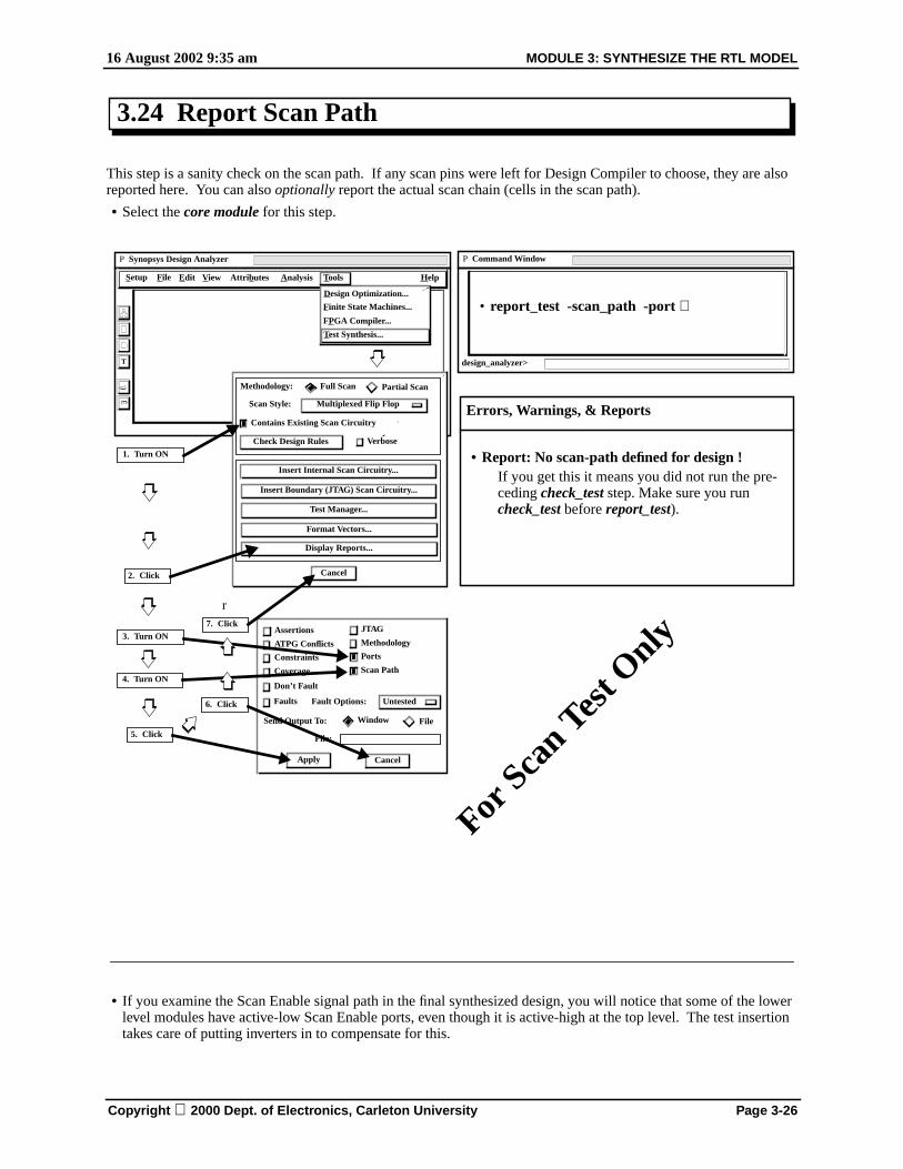
This step is a sanity check on the scan path. If any scan pins were left for Design Compiler to choose, they are alsoreported here. You can also optionally report the actual scan chain (cells in the scan path).
• Select the core module for this step.
• If you examine the Scan Enable signal path in the final synthesized design, you will notice that some of the lowerlevel modules have active-low Scan Enable ports, even though it is active-high at the top level. The test insertiontakes care of putting inverters in to compensate for this.
3.24 Report Scan Path
P Synopsys Design Analyzer
È
È
T
P Command Window
• report_test -scan_path -port ↵
design_analyzer>
• Report: No scan-path defined for design !If you get this it means you did not run the pre-ceding check_test step. Make sure you runcheck_test before report_test).
Copyright 2000 Dept. of Electronics, Carleton University Page 3-26
16 August 2002 9:35 am MODULE 3: SYNTHESIZE THE RTL MODEL
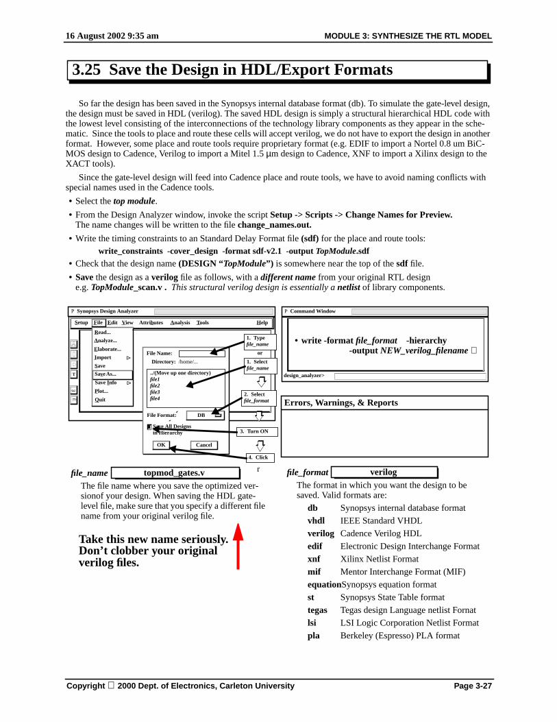
So far the design has been saved in the Synopsys internal database format (db). To simulate the gate-level design,the design must be saved in HDL (verilog). The saved HDL design is simply a structural hierarchical HDL code withthe lowest level consisting of the interconnections of the technology library components as they appear in the sche-matic. Since the tools to place and route these cells will accept verilog, we do not have to export the design in anotherformat. However, some place and route tools require proprietary format (e.g. EDIF to import a Nortel 0.8 um BiC-MOS design to Cadence, Verilog to import a Mitel 1.5 µm design to Cadence, XNF to import a Xilinx design to theXACT tools).
Since the gate-level design will feed into Cadence place and route tools, we have to avoid naming conflicts withspecial names used in the Cadence tools.
• Select the top module.
• From the Design Analyzer window, invoke the script Setup -> Scripts -> Change Names for Preview.The name changes will be written to the file change_names.out.
• Write the timing constraints to an Standard Delay Format file (sdf) for the place and route tools:write_constraints -cover_design -format sdf-v2.1 -output TopModule.sdf
• Check that the design name (DESIGN “TopModule”) is somewhere near the top of the sdf file.
• Save the design as a verilog file as follows, with a different name from your original RTL designe.g. TopModule_scan.v . This structural verilog design is essentially a netlist of library components.
file_nameThe file name where you save the optimized ver-sionof your design. When saving the HDL gate-level file, make sure that you specify a different filename from your original verilog file.
topmod_gates.v
Take this new name seriously.Don’t clobber your originalverilog files.
Errors, Warnings, & Reports
File Name:
Directory: /home/...
Save All Designsin Hierarchy
File Format:
../(Move up one directory)file1file2file3file4
DB
OK Cancel
Read...
Analyze...
Elaborate...
Save
Save As...
Save Info ∆
Plot...
Quit
Import ∆
4. Click
r
1. Typefile_name
1. Selectfile_name
2. Selectfile_format
or
3. Turn ON
file_formatThe format in which you want the design to besaved. Valid formats are:
db Synopsys internal database format
vhdl IEEE Standard VHDL
verilog Cadence Verilog HDL
edif Electronic Design Interchange Format
xnf Xilinx Netlist Format
mif Mentor Interchange Format (MIF)
equationSynopsys equation format
st Synopsys State Table format
tegas Tegas design Language netlist Fornat
lsi LSI Logic Corporation Netlist Format
pla Berkeley (Espresso) PLA format
verilog
Copyright 2000 Dept. of Electronics, Carleton University Page 3-27
16 August 2002 9:35 am MODULE 3: SYNTHESIZE THE RTL MODEL
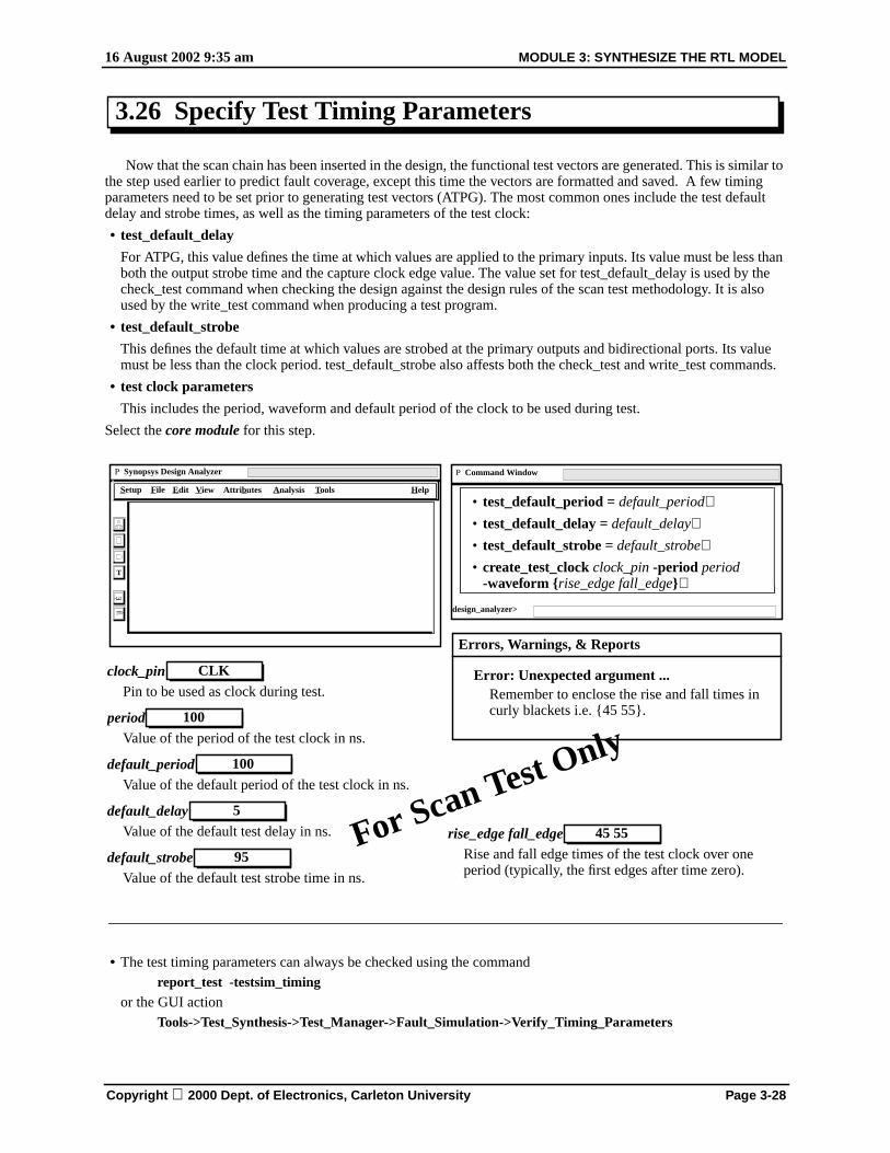
Now that the scan chain has been inserted in the design, the functional test vectors are generated. This is similar tothe step used earlier to predict fault coverage, except this time the vectors are formatted and saved. A few timingparameters need to be set prior to generating test vectors (ATPG). The most common ones include the test defaultdelay and strobe times, as well as the timing parameters of the test clock:
• test_default_delay
For ATPG, this value defines the time at which values are applied to the primary inputs. Its value must be less thanboth the output strobe time and the capture clock edge value. The value set for test_default_delay is used by thecheck_test command when checking the design against the design rules of the scan test methodology. It is alsoused by the write_test command when producing a test program.
• test_default_strobe
This defines the default time at which values are strobed at the primary outputs and bidirectional ports. Its valuemust be less than the clock period. test_default_strobe also affests both the check_test and write_test commands.
• test clock parameters
This includes the period, waveform and default period of the clock to be used during test.
Select the core module for this step.
• The test timing parameters can always be checked using the commandreport_test -testsim_timing
or the GUI actionTools->Test_Synthesis->Test_Manager->Fault_Simulation->Verify_Timing_Parameters
rise_edge fall_edgeRise and fall edge times of the test clock over oneperiod (typically, the first edges after time zero).
45 55
Copyright 2000 Dept. of Electronics, Carleton Univ
ersity Page 3-28
16 August 2002 9:35 am MODULE 3: SYNTHESIZE THE RTL MODEL
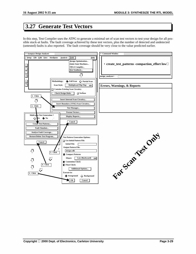
In this step, Test Compiler uses the ATPG to generate a minimal set of scan test vectors to test your design for all pos-sible stuck-at faults. The fault coverage achieved by these test vectors, plus the number of detected and undetected(untested) faults is also reported. The fault coverage should be very close to the value predicted earlier.
Copyright 2000 Dept. of Electronics, Carleton University Page 3-29
16 August 2002 9:35 am MODULE 3: SYNTHESIZE THE RTL MODEL
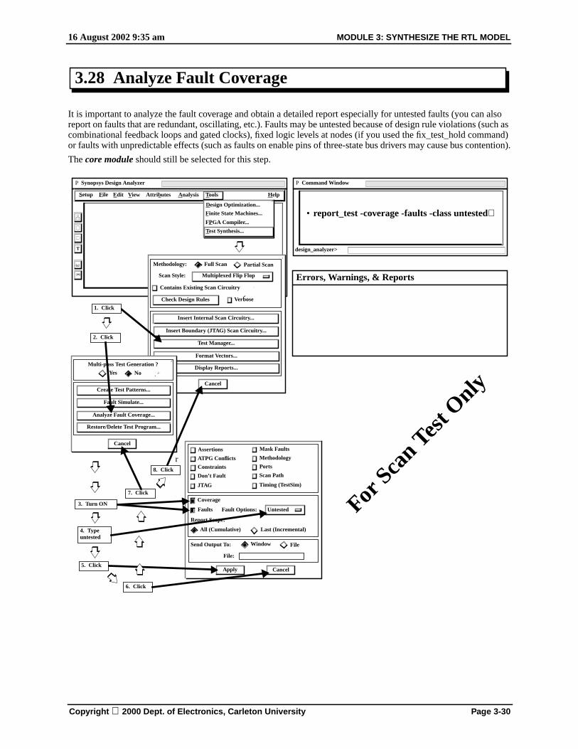
It is important to analyze the fault coverage and obtain a detailed report especially for untested faults (you can alsoreport on faults that are redundant, oscillating, etc.). Faults may be untested because of design rule violations (such ascombinational feedback loops and gated clocks), fixed logic levels at nodes (if you used the fix_test_hold command)or faults with unpredictable effects (such as faults on enable pins of three-state bus drivers may cause bus contention).
The core module should still be selected for this step.
Copyright 2000 Dept. of Electronics, Carleton University Page 3-30
16 August 2002 9:35 am MODULE 3: SYNTHESIZE THE RTL MODEL
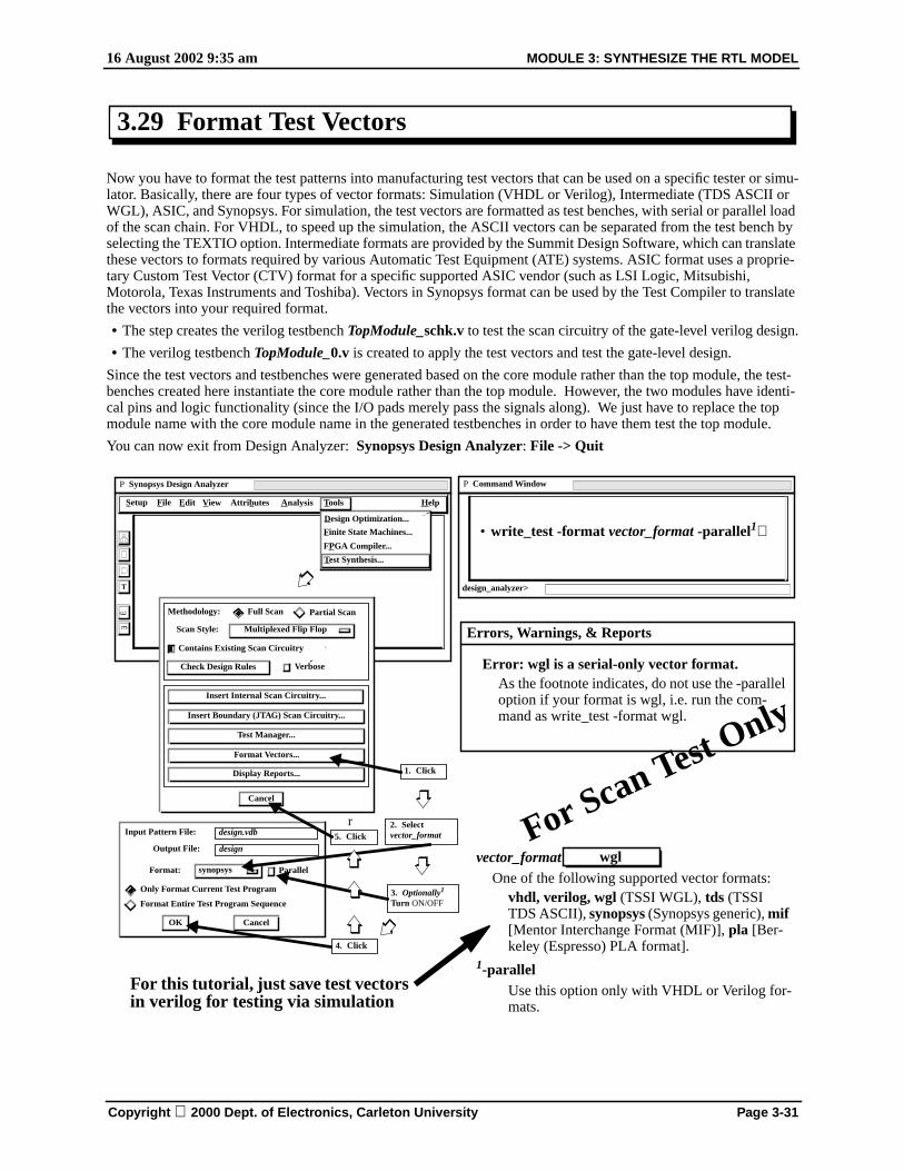
Now you have to format the test patterns into manufacturing test vectors that can be used on a specific tester or simu-lator. Basically, there are four types of vector formats: Simulation (VHDL or Verilog), Intermediate (TDS ASCII orWGL), ASIC, and Synopsys. For simulation, the test vectors are formatted as test benches, with serial or parallel loadof the scan chain. For VHDL, to speed up the simulation, the ASCII vectors can be separated from the test bench byselecting the TEXTIO option. Intermediate formats are provided by the Summit Design Software, which can translatethese vectors to formats required by various Automatic Test Equipment (ATE) systems. ASIC format uses a proprie-tary Custom Test Vector (CTV) format for a specific supported ASIC vendor (such as LSI Logic, Mitsubishi,Motorola, Texas Instruments and Toshiba). Vectors in Synopsys format can be used by the Test Compiler to translatethe vectors into your required format.
• The step creates the verilog testbench TopModule_schk.v to test the scan circuitry of the gate-level verilog design.
• The verilog testbench TopModule_0.v is created to apply the test vectors and test the gate-level design.
Since the test vectors and testbenches were generated based on the core module rather than the top module, the test-benches created here instantiate the core module rather than the top module. However, the two modules have identi-cal pins and logic functionality (since the I/O pads merely pass the signals along). We just have to replace the topmodule name with the core module name in the generated testbenches in order to have them test the top module.
You can now exit from Design Analyzer: Synopsys Design Analyzer: File -> Quit
3.29 Format Test Vectors
P Synopsys Design Analyzer
È
È
T
P Command Window
• write_test -format vector_format -parallel1↵
design_analyzer>
vector_formatOne of the following supported vector formats:
1-parallelUse this option only with VHDL or Verilog for-mats.
wgl
Error: wgl is a serial-only vector format.As the footnote indicates, do not use the -paralleloption if your format is wgl, i.e. run the com-mand as write_test -format wgl.
For this tutorial, just save test vectorsin verilog for testing via simulation
Copyright 2000 Dept. of Electronics, Carleton University Page 3-31
16 August 2002 9:35 am MODULE 3: SYNTHESIZE THE RTL MODEL
Changing the Test Bench for Scan Testing
By the end of this synthesis flow, your design will mapped to technology-specific gate-level cells with extra cir-cuitry for scan testing, etc.. This means it will have extra ports for scan-in, scan-out, and scan-enable pins. You willalso find that any arrayed signals will not be arrayed in the synthesized design; instead, the array elements will belisted as separate signals. You need to examine the format of the array signals in the synthesized (ie. gate-level)design and modify your original testbench for the RTL design to accomodate these changes, then save it under a dif-ferent name e.g. “GateLevel_Testbench”. When the next simulate the gate-level design, be sure the testbench is thefirst file in your verilog command:
This assumes that the ‘timescale is specified in the testbench rather than the second file. It makes sense for ‘times-cale to be in the testbench because:
• the time step resolution is determined by the desired simulation rather than the synthesized hardware.
• the time delay units should only be used in the testbench, since that is the only place where the user should be arbi-trarily controlling the timing of signals. Time delays caused by the synthesized hardware should be completelydetermined by the cell models rather than the user.
In addition to the required revisions to the original testbench, the synthesis procedure will also produce two test-benches in Step 3.28 for scan testing: one to test the scan chain itself, and another to test functionality of the synthe-sized design. Each of these testbenches needs a ‘timescale statement inserted. These can be copied from either theRTL-level testbench or the gate-level testbench (there is no reason why the two should have different timescales).
What To Do
3.30.1 Copy the synthesized design and the scan testbenches of Step 3.28 into the HDLs directory with helpfullyidentifying names.
3.30.2 Perform the gate-level simulation using on your synthesize circuit using the modified gate-level testbenchbased on your original RTL-level testbench. Compare simulations results with the original RTL-level simu-lation. They should be functionally the same.
3.30.3 Run each of the two testbenches from Step 3.28 after modifying them to invoke the top level wrapper andinserting timescale statements. They produce no waveforms, but they do spit out a message telling youwhether the synthesize design is functionally correct.
3.30 Testing the Synthesized Design
Copyright 2000 Dept. of Electronics, Carleton University Page 3-32
16 August 2002 9:16 am Module 4: FLOORPLANNNING
RTL Simulation
Scan Insertion
Gate-Level Simulation
Routing & TimingVerification
Placement
Floorplanning
Clock Tree Generation
Physical Verification
Verilog
DesignAnalyzer
Verilog
DesignPlanner
DP/Qplace
DP/CTGen
SiliconEnsemble
DFII
Synthesis DesignAnalyzer
Module 4: FLOORPLANNNING
Objective :
To create a floorplan for the design including a default group of cells, I/O ringconnected by abutment, and defined placement sites for all cells
You are now starting the physical portion of IC design. This section uses theCadence tool Physical Design Planner (PDP or DP) for physical placement ofa design.The creation and placement of groups is not fully explored in this designexample since it does not contain any macro-cells such as RAM or hard-cores.
4.1 Using Netscape for Online Help
We will be performing a number of cell positioning functions from the areaPdp--Editing window via pop-up panels. Naturally, you will wonder what many of theparameters mean. Most of the panels have a help button which warps yournetscape browser the the right help page. Netscape can get confused and notallow you to scroll down to see all of the help page. Press the Reload buttonseveral times to fully load the help page.
The help button on the Pillar window warps netscape to a central Design Plannerpage, from where you can access the Design Planner Reference PDF document(the index link is not up to date, so use the PDF document!).
4.2 Import the gate-level list
4.2.1 If link dp/tech doesn’t already exist, create it by going into directory "dp"and entering the Unix command:
4.2.2 Make sure there is a startup file local.dpux in the dp/run/ directory asdescribed in “Startup Files for Synthesis and Place & Route” on page v.
4.2.3 To start Design Planner you should be in the dp/run/ directory andshould type the following command at the Unix prompt:
areaPdp &
This will start areaPdp, the timing-driven floorplanning tool. After thetool starts (this may take a minute or two) the Pillar Command windowand the log window should both appear.
Copyright 2000 Dept. of Electronics, Carleton University Page 4-1
16 August 2002 9:16 am Module 4: FLOORPLANNNING
4.2.4 To import your design from a Verilog netlist into a Design Planner library, from the Pillarwindow, select the following menu pick:
File->Import->Verilog...
This brings up the ver2hld and View File windows.
4.2.5 Select or enter the following values in the ver2hld form:
Input Verilog file names: ../../HDLs/TopModule_gates.v(assuming this is filename and location of the gate-level netlist)
Press Print informational messagesName of Top cell to translate: TopModulePress Name of the global netsPower: VDDGround: VSSTie nets (up down): VDD VSS (Press the button before specifying VDD VSS)Output library name: designCreate primitives with view name: abstract (Press)Create blocks with view name: autoLayout (Press)
OK the ver2hld form to import your Verilog netlist.
It may take a while to complete, but no errors or warnings should be produced. You canQuit the View File window.
4.2.6 In the Pillar window select:
File -> Open...
4.2.7 In the Open File window select:
Libraries -> designSelect TopModule, and click OKSelect autoLayout and click OK
This should launch the areaPdp--Editing window.
In the editing window you should see your I/O pads and standard cells piled on top of each other.You should turn on visibility of the cell instance names by selecting
View->Preferences-->Show->Instance Text: Instance Name
4.3 Reference Data for I/O Pads via netscape
The next step is to add power cells to your design. The pad cell (and core cell) descriptions for thistarget 0.35 micron process can be viewed with netscape. Go to the web page file:/CMC/kits/cmosp35/doc/cmosp35_docs.html .
Copyright 2000 Dept. of Electronics, Carleton University Page 4-2
16 August 2002 9:16 am Module 4: FLOORPLANNNING
• Under "CMOSP35: STANDARD CELL LIBRARIES", follow the link Standard Cells and3.3V and 5V I/O’s under the Black-Box Libraries list .
• At this point, curious users may wish to detour to the link Simple Guidelines for Using tsmc0.35um Libraries and glance at the overview of the cell libraries.
• Otherwise, under "3.3V I/O", follow the Typical Case link for a list of pads for theTPD773PN library. Each one has its own web page.
• Note that non-I/O-pad cells (those in the core module) are listed under "Standard Cells"instead of "3.3V I/O"
4.4 Add power pads to the design
In areaPdp, the power supply pad cells are added as an ECO (engineering change order) since thecells do not exist in your current netlist i.e. adding these cells will modify the netlist.
4.4.1 Select ECO -> Cells -> Add with Connectivity...
Note that we are adding four core pairs (pairs of VDD/VSS power pads for feeding thecore circuit), and six ring pairs (pairs of power pads for feeding only the I/O buffer padsthat form a perimeter around your core design). From the HTML datasheets for theCMOSP35 tpd773pn library pads, see that PVDD1 has a core power connection, PVDD2has I/O (or ring) power connections, and PVDD3 has both core and ring connections.
4.4.2 In the Design Planner Glue Cell Addition form enter/modify:
You should see four new I/O cells added to your workspace (press Fit in the area-Pdp--Editing form if necessary).
4.4.3 Adding PVSS1 cells follow a similar procedure.
Change:
Cell Name: PVSS1Prefix Name: vss_core
Click Apply
4.4.4 Repeat again for six pairs of ring (I/O) cells using the following form for VDD:
Cell Name: PVDD2Prefix Name: vdd_ring
Copyright 2000 Dept. of Electronics, Carleton University Page 4-3
16 August 2002 9:16 am Module 4: FLOORPLANNNING
Number to Add: 6
Click Apply
4.4.5 The PVSS2 cells follow the same convention.
Change:
Cell Name: PVSS2Prefix Name: vss_ring
Click Apply
4.4.6 Once all power pads have been added, Close the Design Planner Glue Cell Additionwindow.
4.5 Initialize the floorplan
4.5.1 The design floorplan is ready to be initialized.
In the areaPdp--Editing window select:Floorplan -> Initialize...
4.5.2 In the Design Estimation Parameters form, change:
Estimate Aspect Ratio [X/Y]: 1.5Standard Cell Routing Ratio: 0 Press Area?Click Apply & Close the form
You should now see a die area with the specified aspect ratio. Your core cells should col-lected be at the lower right, while power pad and I/O pads are spread out along the top.
4.5.3 Corner cells are needed to connect the I/O rings. They are added next.
In the areaPdp--Editing window, select:Place -> I/O -> Corner Cells -> Add...
4.5.4 Fill out the Design Planner Add I/O Corners form by selecting:
I/O Corner[BL] and add the following information:Library Name: tpd773pnCell Name: PCORNERView Name: abstract
4.5.5 Now select the remaining I/O Corner[BR], I/O Corner[TR] and I/O Corner[TL] andcopy and paste the entries across to the other boxes so all four corners are filled out thesame.
4.5.6 Apply & Close the Design Planner Add I/O Corners form.
Copyright 2000 Dept. of Electronics, Carleton University Page 4-4
16 August 2002 9:16 am Module 4: FLOORPLANNNING
4.5.7 Placing the I/O tends to be problematic, so this is a good place to save an intermediate ver-sion of your design. From the AreaPdp--Editing window select:
File -> Save As...
4.5.8 In the Save File As form enter:
Save as: initializedClick OK
If something goes wrong with I/O placement, you can load this intermediate version andtry again.
4.6 Create the ring of I/O cells
Your floorplan should now have placed corners. The remaining I/O cells will now be arranged intoa ring of butted pads. Creating a proper I/O floorplan is one of the most critical steps in the digitaldesign process, partly because it is the boundary condition driving place and route. To bephysically realizable as a ring formed from abutment, you must ensure opposite sides of the ringare the exact same size. Other areas of concern to the user are: Is the I/O pad to I/O pad pitchcompatible with the selected bonding process? Will the die fit within a selected package? Have anadequate number of core and ring power pairs been added to the design?
For the purposes of this lab, you can copy the pad placement file MyPlacement.ioc from thesamples directory and skip Step 4.6.2 below; it deals with creating your own pad placement file.If you skip that step, you would also avoid doing the sections after Step 4.6.3 dealing with how toorganize pads, though it is highly advisable to read it. Also, in order to do Step 4.6.3, you still haveto examine the placement file to get an idea of how pad order is specified.
Generate an initial I/O placement file for your design
This initial I/O placement will consist of randomly ordered pads abutted into a ring. It merelyserves as a starting point which must be modified to meet external requirements, such as bondingmachine limitations and packaging availability.
4.6.1 In the areaPdp--Editing window select:
Place -> I/O -> Pads/Pins...
For the reasons mentioned above, It’s recommended that you skip to 4.6.3.
4.6.2 Modify the Design Planner Place I/O Initialize form as listed:
I/O Init Mode: print random io fileI/O Init File Name: random.iocI/O Init I/O boundry Mode: generate newI/O Init I/O to I/O Min Distance: 0.0
Copyright 2000 Dept. of Electronics, Carleton University Page 4-5
16 August 2002 9:16 am Module 4: FLOORPLANNNING
Click Apply
A random.ioc file should be created.
All the fields of the Design Planner Place I/O Initialize form have verbose and puzzlingnames starting with the words "I/O Init". This prefix is merely a reminder of the formname. The help pages (and the form itself) make more sense if you ignore this prefix.
To view the pads as a ring, the random.ioc placement file must be read. This is the nextstep.
Read a Pad Placement File
4.6.3 In the Design Planner Place I/O Initialize form, enter:
I/O Init Mode: load fileI/O Init File Name: Your_Pad_Placement_File_Name e.g.: ../../samples/BlahBlah.iocI/O Init I/O boundry Mode: generate newI/O Init I/O to I/O Min Distance: 0.0 <== Important for abuttment ****
Make sure the I/O Side Ordering field matches the direction of pad ordering specified inthe placement file.
Click Apply
The pads should now be organized into a ring with the pad cells butting up along the entire ring,except maybe at the corners. Zoom in as close as possible to an abutment edge until you can seethe discretized motion of the focus point as your mouse moves around. Since this is the limit ofpositional resolution, it confirms that the cells are abutted.
If the pads overlap rather than but-up, then the I/O to I/O Min Distance field in the DesignPlanner Place I/O Initialize form was probably left at its default value -1.0. Set it to 0.0, as above,and load the placement file again.
If you mistakenly left the test_so pins in the design, the pad instance will be left in its originalposition and not be incorporated into the ring. This is because its position is not specified in theplacement file. Remove it from the RTL source files and start this lab over.
Organization of I/O Pads
Zoom out, click on various pads, and look at their names at bottom of the areaPdp--Editing form.Remember to have instance names turned on. As expected, there is no rhyme or reason to theplacement of the randomly ordered pads. The pad positions must now be reorganized to meet real-world needs, as well as to ensure a continuous and unbroken ring.
One likely requirement to be met is the minimum spacing that can be handled by your bondingmachine. It is possible that you have to space the pads out at a sparser pitch, in which case "feeder"
Copyright 2000 Dept. of Electronics, Carleton University Page 4-6
16 August 2002 9:16 am Module 4: FLOORPLANNNING
cells of the appropriate size are required between pads to maintain continuity of the ring. Feedercells are also used to maintain ring continuity when the design is core bound i.e. when the core areais so large and the number of pads so small that there are not enough pads to form a continuousring around the core.
For the purposes of this tutorial, we briefly go over some considerations for proper pad placement.We will not actually go through the I/O floorplan.
Use a text edittor to view the I/O placement file random.ioc. Helpful comments are shown usingsemicolons (’;’). The corner cells are show at the top. The lists of pads along each edge of the I/O boundary are designated by T, R, B, and L (top, right, bottom, and left edges). The direction ofpad placement along each edge is specified by the I/O Side Ordering field of the Design PlannerPlace I/O Initialize form. Knowing this, it is a simple matter to move the pads around. It isespecially simple in this example, where all the pads are the same size. The Black Box cell libraryis pretty good that way; all the pad widths are integer multiples of a minimum pad width.
Some basic considerations in where to place pads are:
• Place "ring" power and ground in the corrner of the I/O ring, since no traces need to be routedto them. (PVDD2 and PVSS2)
• Place "core" power and ground away from the corners of the I/O ring so traces can be rundirectly from the power pad to the core power ring without the need for bends. This is espe-cially important for small designs, where the power bus width is so large compared to theavailable routing space that an careening power bus can prevent proper routing for the remain-ing signal lines.
• It is generally believed to be a bad idea to mix core and ring power (PVDD3 and PVSS3).However, if you do use these for some reason, place them near the center of the I/O ring, thesame as the PVDD1’s.
• When loading your pad placement file, use load file rather than load file&auto place so thatyou know the entire file was properly read (mistyped pad names are not placed).
Justify your I/O placement
If opposite sides of the die have equal total widths of abutted pads, with the only gap between thepads and the corners, then this step should push them all together into a continuous ring.
4.6.4 From the areaPdp--Editing window select:
Place -> I/O -> Justify...
4.6.5 In the Design Planner Place I/O Justify form set:
I/O Corner to I/O Distance: 0.0
Copyright 2000 Dept. of Electronics, Carleton University Page 4-7
16 August 2002 9:16 am Module 4: FLOORPLANNNING
Click Apply & Close
You may get an error related to the Boundary and other "Info’s". Close inspection is thebest way to tell whether the I/O ring is OK.
This last step should ensure your I/O ring is properly connected by abutment. You should visuallycheck that there are no gaps in the I/O ring. To do this, zoom in on the I/O ring, and pan around thedesign.
If there are any problems, or required changes to your I/O ring, you can repeat the initialize I/Ostep, and subsequent steps. You do not need to add corner cells again (once they have been addedto your design).
Copyright 2000 Dept. of Electronics, Carleton University Page 4-8
16 August 2002 9:16 am Module 4: FLOORPLANNNING
Figure 4-3 illustrates many of the steps you’ve taken so far. Feeder cells are also shown for thecase that the pads need to maintain a minimum spacing for a specific bonding machine. Thesubsequent steps will complete this diagram.
Before proceeding, you may want to save the state of the design using a helpful name, like"JustifiedPads".
4.7 Define and place groups
Once you are happy with the I/O ring, you can prepare to place your standard cells.
Most designs which do not contain macro cells and are smaller than 500,000 cells should be placedflat. This allows the timing-driven features of the placement and routing tools to ensure critical netsmeet timing.
Default
Sets of four 20-micron wide feeder cells
I/O and power cells
Corner Cells
Default group of unplaced cells created byFloorplan -> Groups -> Generated by Logic...
User-drawn region of rows
Estimated core area generated by Initialized floorplanplaced inside the core withPlace -> Blocks/Groups (Leggo) ...
Figure 4-3: Floorplanned design.
Copyright 2000 Dept. of Electronics, Carleton University Page 4-9
16 August 2002 9:16 am Module 4: FLOORPLANNNING
If your design contains pre-placed blocks (hard cores) they are also floorplanned at this step.
This section is composed of two main parts. In the first part, areaPdp collects the cells into groupsin order to facilitate high level organization of large chunks of the circuit in the second part. Thisexample design will have just one group, as shown in Figure 4-3, delineated by a yellow boxencompassing the cells for the group. The proportion of space within the group which will beoccupied by cells is called the area utilization. Lower utilization means more free space, greaterflexibility in organizing and interconnecting the cells, and higher likelihood of meeting constraints,at the cost of more area for the group.
The second part defines a core region in which to organize groups (just one in our case). Here,utilization is used again to refer to the excess space within the core area in which to organize andinterconnect groups.
4.7.1 To create groups based on logic, from the areaPdp--Editing window select:Floorplan -> Groups -> Generate by Logic...
If your design imported from Synopsys contains more than one level of hierarchy withinthe core, you can flatten it here by selecting Cells/Group Min: 100,000. This will ensureall groups are at least 100,000 cells large.
4.7.2 Select:
Utilization Pin Grid (um): 1.4Click Apply.
This should create one group of cells called default located outside of your die area.Zoom in to take a close look. Your group has the default area utilization of 75%. Thismeans only 75% of the total area available for placing cells in that group is actually cellarea, and the remaining 25% unused area can be used for adding power striping, spacebetween rows of cells, space for adding clock tree buffers, and to reduce routing conges-tion. Try entering different values for utilization and pressing Apply. The group sizeshould change to give more or less free space within the group. Experience will make youa better judge of what utilization factor is best. Since this example is small, 55% utiliza-tion was specified to avoid placement anomalies. Since the design is pad limited, there isso much wasted core area that there is no point in trying to achieve greater utilization.
Close the Logic Group Options form when you’ve applied a suitable utilization.
4.7.3 To place the group(s):
Select Place -> Blocks/Groups
4.7.4 In the Design Block/Group Placement form:
Click Apply to have your block reshaped and placed in the core (sometimes this reshapingwill not happen - this is not a problem). Be sure that your default group (yellow box) iswithin the marked core area, otherwise you may have problems in Qplace. Exceeding the
Copyright 2000 Dept. of Electronics, Carleton University Page 4-10
16 August 2002 9:16 am Module 4: FLOORPLANNNING
core area by only 10% will definitely cause errors in Qplace.
If the default group cannot be placed inside the core area:
Select Adjustable Core Area(%): 10.0Apply again
4.7.5 Close the Design Block/Group Placement form
4.8 Create placement sites
Creating rows of placement sites
The placement tools require rows of possible placement sites where the I/O and core cells will beplaced. Since the I/O’s are already placed, the I/O rows are generated from the preplaced I/O’s.The core placement rows are generated in a manually drawn region which is just larger than yourplaced block. If you had more than one placed block, your region of rows would have to cover allof the placed blocks in your core area.
4.8.1 From the areaPdp--Editing window, select:
Floorplan -> Rows -> Create I/O Rows...
In the Design Planner Draw I/O Site form select:
Site Name: padFrom Preplaced IOs (Press)
Click Apply & Close.
Redlines show the "I/O Rows".
4.8.2 To create a region of cell placement site rows, select:
Floorplan -> Rows -> Create Region of Rows...
Your design might be I/O bound, in which case there is lots of cell area, rows will beplaced with VDD rails at the top, VSS at the bottom, and a gap between the rows. If spaceis more of an issue, every second row can be inverted so the rails are abutted, and no gap isrequired between rows.
4.8.3 In this step you will be drawing a box around the core of your design (see dotted box inFigure 4-3). Before proceeding you may wish to zoom-in on the core area of your designby drawing a box around the core using the right-hand mouse button. You should be ableto see all of the default group (yellow box containing green standard cells) before proceed-ing.
In the Design Planner Draw Site Region form select:
Channel Offset Offset: 1.25
Copyright 2000 Dept. of Electronics, Carleton University Page 4-11
16 August 2002 9:16 am Module 4: FLOORPLANNNING
Click Apply & Close
4.8.4 The bottom of your areaPdp--Editing window should now say:
Please Specify Point 1 for Region—The tool wants you to define the region which isfilled by rows. If your default group (yellow box) is totally within the marked core area,you can draw the region larger than the group, but smaller than the core. If the group ispartially outside your core area, draw the region just slightly larger than the default group.Once you’ve decided where to draw your region, click once to mark the upper left cornerof the region, and once to mark the lower right (see Figure 4-3).
4.8.5 If you are not happy with your region of rows, you either
re-start from your most recently saved design (Strongly recommended).
Or, you can delete it with: (NOT Recommended)
Floorplan -> Rows -> Delete...
and try again. Those who are paranoid may wish to save the design as (say) "Defined-Rows" once you get a decent row delineation.
4.9 Define special nets
4.9.1 The last step in floorplanning is to tell the tool which are the special nets in your design.
From the areaPdp--Editing window select:Floorplan -> Nets -> Setup Special Nets...
4.9.2 In the Special Net Connectivity form, enter the following settings:
Match Name? ONNet Name? clk or use Browse to select the root clk net*
Net Type: clockClick on Set By Net TypeClick on Set Name Net Type
* This should be the clock port name of the wrapper and core modules.
4.9.3 In the same form, set up for VDD:
Net Name? VDDNet Type: supplyClick on Set Name Net Type
In the DEF Print Properties section,
Net name? VDD
Ensure Special is set to (* VDD)
Copyright 2000 Dept. of Electronics, Carleton University Page 4-12
16 August 2002 9:16 am Module 4: FLOORPLANNNING
Click on Set Net Properties
4.9.4 Repeat the above steps for VSS.
Net Name? VSSNet Type: groundClick on Set Name Net TypeIn the DEF Print Properties section,Net name? VSSChange Special to (* VSS)Click on Set Net Properties
Click on Print Special Connectivity Summary to View File
We have provided an example of a Summary for your reference.
# Special Net Connectivity Summary, May 11 16:57:30 1999# Cell (design TopModule autoLayout)# Net clk, Type clock# Net VSS, Type ground# Net VDD, Type supply(DEFSPECIAL_CONN (NET VDD (SPECIAL_SUM (SPECIAL (INST_TERMS 2136) (ROUTE_SHAPES 0 ) ) ENDSPECIAL_SUM) (DEF_SPECIALNETS "( * VDD )" ) ENDNET) (NET VSS (SPECIAL_SUM (SPECIAL (INST_TERMS 2136) (ROUTE_SHAPES 0 ) ) ENDSPECIAL_SUM) (DEF_SPECIALNETS "( * VSS )" ) ENDNET)ENDDEFSPECIAL_CONN)
Note the INST_TERMS numbers will likely differ in your design from those shownabove. I also found that if I mistakenly left test_so in design and blindly forged aheadwith the pad ring, there will be anomalous (extra) entries in the NET VDD/VSS blocks.
4.9.5 Close the Special Net Connectivity form and Quit the ViewFile form.
4.10 Add power stripes (power planning)
Before the standard cells are placed, you need to add power stripes, each of which consists of aVDD and VSS bus. These stripes, along with the power rails built into each standard cell, form a
Copyright 2000 Dept. of Electronics, Carleton University Page 4-13
16 August 2002 9:16 am Module 4: FLOORPLANNNING
power and ground grid. The stripes are placed but not connected before the cells are placed soQplace (the timing-driven placement engine) knows to avoid placing cells under the power stripes.
4.10.1 To add power stripes through your design, select:
Floorplan -> Preroutes -> Supply Stripes...
4.10.2 Modify the Design Planner Route Stripes form as follows:
Net Name(s): VDD VSSLayer: metal2Width(s): 3.2 3.2 Spacing 1.0Start Position: 10.4Number of Stripes: 3Apply & Close
Metal2 is selected for the stripes since it is the default metal for vertical routing (metal1 &metal3 are default for horizontal routing).
Three stripes were chosen above just to illustrate how multiple stripes are automaticallyinserted at a fixed pitch. For example, if the core is approximately 800 microns across,starting the first stripe at 200 microns will divide the core into approximately four equalsections. The number and spacing of stripes is dependent on the shape/size of your coreand your power distribution requirements.
Stripe Positioning
The Widths of 3.2 and Spacing of 1.0 are selected to keep the center of the busses on the 1.4-micron routing grid. The Start Position specifies where to put the first and last stripes relative tothe edge of the Region of Rows. It is only a rough positioning as specifies the position of the centerof the first bus (VDD) of the stripe relative to some unseen position slightly beyond the Region ofRows (in this example, it is half the routing grid spacing beyond i.e. 0.7 micron). Since the bussesare constrained to lie totally within the Region of Rows, a Start Position of 0 micron will hard-limit the position of the edge-most bus to be flush with the Region of Rows boundary.
If the Widths, Spacing, and Start Position do not leave the busses on the 1.4 micron grid, theirpositions will be adjusted to center them on the grid; the actual Start Position may be slightly less(or more) than specified. The actual Spacing will always be at least as large as specified, exceptin the pathological case where a bus is hard-limited against the Region of Rows boundary. In thiscase, the partner bus for that stripe is positioned as if there was no hard-limiting, leaving lessSpacing than specified. To avoid this, Start Position should be well away from the boundary.
4.10.3 If you wish to re-do the stripes and/or rings, you can Edit -> Delete All Routing... andthen repeat the last step.
Copyright 2000 Dept. of Electronics, Carleton University Page 4-14
16 August 2002 9:16 am Module 4: FLOORPLANNNING
Since this particular example design is very small, it only makes sense to have one stripe.
Delete all the three stripes inserted above and insert one stripe down the center.
You can use the cursor to figure out how far from the edge of your "region of rows" to therough centre of your design. It should be about 70 - 80 um.
Figure 4-4 shows what the design should look like.
4.10.4 Save the design at this point. You have now completed floorplanning.
File -> Save As...Save as: floorplan
THIS IS A NATURAL BREAK POINT
Copyright 2000 Dept. of Electronics, Carleton University Page 4-15
16 August 2002 9:16 am Module 4: FLOORPLANNNING
Figure 4-4: Example of how floorplanned design should look like.
Copyright 2000 Dept. of Electronics, Carleton University Page 4-16
16 August 2002 9:35 am MODULE 5: TIMING-DRIVEN PLACEMENT OF STANDARD CELLS
RTL Simulation
Scan Insertion
Gate-Level Simulation
Routing & TimingVerification
Placement
Floorplanning
Clock Tree Generation
Physical Verification
Verilog
DesignAnalyzer
Verilog
DesignPlanner
DP/Qplace
DP/CTGen
SiliconEnsemble
DFII
Synthesis DesignAnalyzer
MODULE 5: TIMING-DRIVEN PLACEMENT OF STAN-DARD CELLS
Objective:
To use forward-annotated timing information from Synopsys to place the core
cells.
5.1 Use the QPlace sequencer
5.1.1 To bring up the placement sequencer, from the areaPdp--Editing win-dow select:Place -> Blocks/Cells (QPlace)...
In the Qplace Sequencer, select Sequencer Setup...
Under Placement (Qplace)Select Placement Options...
5.1.3 In the Qplace Placement Parameters form select:
Prewire Keep Out? (this prevents cells from being placed under thepower stripes.)
Close the Qplace Placement Parameters and Sequencer Setup forms.
5.1.4 In the Qplace Sequencer select:Congestion Map Display
NOTE: There is currently a bug in the Design Planner Sequencer which causesthe sequencer to fail if steps are run one by one, instead of using the sequencer torun all the placement steps at once. Also, since the Qplace sequencer spawns anew Unix shell to run the Qplace tools, your account MUST be set up to use allof the Cadence tools in your .cshrc (or .bashrc) file. If you manually enter acommand line script or use some other means of setting up your account to workwith Cadence tools, it is likely the next step will fail since you will not be giventhe chance to set up the temporary shell used to run Qplace. Naturally, this step
Copyright 2000 Dept. of Electronics, Carleton University Page 5-1
16 August 2002 9:35 am MODULE 5: TIMING-DRIVEN PLACEMENT OF STANDARD CELLS
will also fail if your .cshrc file has an exit command before the statement(s) that sets your Cadenceenvironment.
An important note:
The aformentioned bug will cause 5.1.5 to fail the first time it is run. To solve this problem:
• Ensure you run as in 5.1.5 first -> it will fail in the DEFOUT step, but will create some usefullfiles nonetheless
• Using the unix command prompt, navigate to the ../dp/run directory (if not already there)
• In that directory there is a hidden file called .run_sdf2def (You can see it with an ls -al com-mand.)
• You must run this batch file manually with the command: ./.run_sdf2def
• This will create a file called timing.def (a converted version of your .sdf file) in theFunCount_chip_QP directory
• Go back into the Qplace Sequencer Setup form and remove the check from "Convert SDFConstraints".
• Re-run the sequencer as in step 5.1.5 and everything should go allright.
5.1.5 Click Apply in the Qplace Sequencer
This step insructs Design Planner to:
• create a library description file (LEF) listing the cells included in the design
• create a design file (DEF) containing the cell interconnect information but no place-ment information at this time
• create a timing constraints file based on the .sdf file from Synopsys
• use all these files to call Qplace, the timing-driven placement engine.
Qplace will create a new .def file which is then imported back into Design Planner. Withluck there will be no problems!
Qplace works by placing cells in various sites while trying to minimize the length of netsrequired to connect the cells. When timing-based placement is selected, the nets are given
Copyright 2000 Dept. of Electronics, Carleton University Page 5-2
16 August 2002 9:35 am MODULE 5: TIMING-DRIVEN PLACEMENT OF STANDARD CELLS
weights based on how much timing slack (or negative slack) exists in each net.
5.1.6 Once Qplace has completed, Save your design as placed.
Verify Integrity of Placement
You should now ensure the placement step worked (if not, your future steps will also fail). Oneway to tell is to zoom-in on the core of your design, and see if the cells are now spaced out overthe core area (instead of all packed together as they were in Figure 4-3). You can also view thelog files in the new TopModule_QP directory and ensure there were no errors.
If Qplace had problems placing your cells (e.g. if you specified too high area utilization withinthe group), one possible outcome is a warning about overlapping components during this step. Youmay also see cells protruding beyond the yellow group border, which is not a problem except forfact that it indicates a potentially difficult placement, with the possibility of overlapping of cellselsewheres; you should take extra care to search the log file with an edittor for warnings of overlap.One possible measure against problematic placement is to specify a lower area utilization withinthe group(s). Erase all cell site regions and power stripes before doing this. You will also have tounpress Separate Cells Fixed on the Logic Group Options form to free up the placed cells. Afterredefining and placing the group, recreate the placement sites and add power stripes
5.2 View placement congestionA congestion map will have been imported. This map can be used to determine the esti-mated routing congestion for your design.
5.2.1 You may turn off the site row display if you have the site drawing layer visible. In the Pil-lar window, select:
Environment->Layers...
5.2.2 Under Layer-Purposes select Site Drawing
Deselect visibleClick Redraw
The congestion map display is much easier to read now.
Placement on this design takes about 10 minuteson an Ultra Sparc 10. Your own design will likelytake longer depending on design size, number ofcritical nets, and CPU resources available.
Copyright 2000 Dept. of Electronics, Carleton University Page 5-3
16 August 2002 9:35 am MODULE 5: TIMING-DRIVEN PLACEMENT OF STANDARD CELLS
5.2.3 To view the values that are displayed, zoom in closely on the congested area within thecore. The congestion is displayed using the following format:
5.2.4 To remove the congestion grid, from the QPlace Sequencer click on Options next toCongestion Map Display. In the Congestion Map Display form, click on Clear.
5.3 Perform timing analysis based on initial placement
Before you insert the clock tree, you should perform static timing analysis to ensure that yourplacement will come close to meeting your timing constraints. We use the Pearl timing analysisenvironment to calculate the delays of critical signal paths based on the cell delays and net loading.This is becoming more prevalent for timing verification than verilog simulation, which only teststhe conditions encountered in the simulation. This timing check can also be run a second timefollowing the clock tree generation. Note the estimated delays on the clock net at this point. Dothey change after clock tree insertion?
Provide Timing Analysis Information Using GCF File
The timing analysis needs information about the operating condition of the design, such as clockand external load, as well as information about the target technology/library. This information ispassed to areaPdp using a General Constraint File (GCF file). Look at the samples directory forthe sample GCF file FunCount_chip.gcf; it is a fairly simple file. The first half containsinformation about the target technology and shouldn’t change much between designs. The secondhalf specifies the clock and external load. The line
defines a waveform with 20ns period, positive edge at 0ns, negative edge at 10ns, and labels thiswaveform as "50 MHz 50/50". The "CLOCK" line further down selects this waveform to be theclock to appy to the "clk" node, while the "EXTERNAL_LOAD" line specifies the external loadcapacitance. All of this information corresponds to the constraints set during synthesis (usingDesign Analyzer). For your own design, these values should change to match the synthesisconstraints accordingly.
5.3.1 To begin select Timing->Pearl->Setup Run Environment...
In the DP-Pearl Setup Run Environment window:Change the GCF File to ../../samples/FunCount_chip.gcfClick on Apply & Close.
5.3.2 To begin the timing check, select Timing->Pearl->Check Timing vs. Constraints...
h (6, 10, 20) where 6 is the number of tracks used10 is the number of tracks available20 is the number of tracks for all layers v (6, 10, 20)
Copyright 2000 Dept. of Electronics, Carleton University Page 5-4
16 August 2002 9:35 am MODULE 5: TIMING-DRIVEN PLACEMENT OF STANDARD CELLS
(NOTE: If you have your constraints and timing information captured in a gcf file you canuse the Analyze Timing option from the Pearl menu instead. For more information on thissee the Cadence documentation).
There is a bug that will cause 5.3.3-5.3.6 steps to fail. You can either skip this timinganalysis, or use the Timing->Pearl->Analyze Timing option instead. The window thatpops up is the Pearl Timing Analysis window that can be used to show informationabout various paths through the design.
When you’re done, please skip to Creating A Clock Tree section in Page 6-1
5.3.3 In the DP-Pearl Check Timing vs. Constraints window select:
Display Pearl Graphical InterfaceSet the Create_New_SPF flagChange the Path Constraint Reference Type to SDF, andfile name to ../../Synopsys/FunCount_chip.sdf
5.3.4 Now click on the Pearl Delay/Parasitic Input: Options... button
In the DP-Pearl Create RC Parasitics window, select:Create Using: CDS Steiner TreeOuput As: rSPF
5.3.5 Next click on the Create Using: Options... button
In the Design Planner CDS Steiner Tree RC Option window, make sure the ExtractBoundary Info flag is set on.
Also turn on the Read Congestion Map flag and provide the path to the congestion mapcreated when running Qplace, FunCount_chip_QP/placed.congMap
5.3.6 Click Apply & Close in the Design Planner CDS Steiner Tree RC Option window.
Click Close in the DP-Pearl Create RC Parasitics window.
Click Apply & Close in the DP-Pearl Check Timing vs. Constraints window.
You might get the following warnings in the areaPdp.log window:
• WARNING -*- Via RC information not in tech file
• HLD-WARNING: SPF instance section not generated due to incomplete information
• Warning: Found pearl_library in /CMC/tools/cadence.1999a/IC/tools/pearl/tcl/library, not inCadence installation(This last warning only if you activated Display Pearl Graphical Interface in the DP-PearlCheck Timing vs. Constraints window)
These warnings seem harmless.
Copyright 2000 Dept. of Electronics, Carleton University Page 5-5
16 August 2002 9:35 am MODULE 5: TIMING-DRIVEN PLACEMENT OF STANDARD CELLS
After a short while the Pearl GUI should pop up. It might contain errors about "Latch clausecontains no clock or input" during the "ReadGCFTimingLibraries" activity, which seem harmless.The left hand side window is the Pearl Console window. There should be a right-hand sidewindow showing the worst case possibilities of constraint violations in the Pearl Summarywindow. CMC has also observed an error with some versions of Pearl where the Pearl Console isthe only Pearl window that opens, and it contains an error message: Error: invalid commandname "FindSDFPathConstraints". If you have this in your window, manually enter thecommand: cmd> findpathconstraints in the Pearl Console. This should cause the PearlSummary window to be produced.
The constraints used (set back when using Synopsys) set a maximum time for the data to becomestable. The worst estimated result (least amount of slack time) is #1. If you click on #1 a new setof windows opens up showing a schematic of the path as well as a list of delays through eachcomponent. If you view your PDP design window you will see the path highlighted in yourfloorplan. If you click on any of the components or paths in the schematic or list, the appropriategate or net will also be hightlighted in the floorplan.
You can also experiment with the timingverify, findpathsfrom clk ^, and checklimits commandsas described later in section Step 8.4.
Although minor violations may be corrected by timing-driven routing, the sample design had noproblems at this point.
All timing should easily be met at this point. When you are done close all the Pearl windows,remove the highlighted path(s): select View -> Clear or just click on the Clear button in theareaPdp-Editing window.
Copyright 2000 Dept. of Electronics, Carleton University Page 5-6
16 August 2002 9:16 am MODULE 6: CREATING A CLOCK TREE
RTL Simulation
Scan Insertion
Gate-Level Simulation
Routing & TimingVerification
Placement
Floorplanning
Clock Tree Generation
Physical Verification
Verilog
DesignAnalyzer
Verilog
DesignPlanner
DP/Qplace
DP/CTGen
SiliconEnsemble
DFII
Synthesis DesignAnalyzer
MODULE 6: CREATING A CLOCK TREE
Objective:
To add clock buffer cells and nets to create a balanced clock tree which exceedsthe parameters specified in synthesis. Also, to generate a “golden” Verilognetlist of the design to be used for final verification
Now that the cells have been placed, the clock tree can be created.
6.1 Define the clock tree
A clock tree will be synthesized to replace the existing clock tree. Since Synopsyswas instructed to not touch the clock tree, it currently consists of one net (calledclk_core in the top wrapper module). CT Gen will be told to replace clk_corewith a balanced tree meeting the desired performance criteria.
6.1.1 To define the clock net select:
Place -> Clock -> Setup -> By Name...
6.1.2 In the Design Planner Create Clock form, press the Browse button anddouble-click on the net connecting the clock pad to the core (clk_core).
Then press the Options... button.
6.1.3 In the Design Planner Clock Tree Options form, enter values to matchthe clock specified in Synopsys, but over-constrain the Max Skew by abit. Note the I/O instance name of the clock input pad is clk_ip from theoriginal rtl.v file, and the output pin of that cell is C from the I/O cellhtml data files.
Enter:
Clock Root Driver: clk_ip (the instance name of FunCount_chip’s clockinput pad)Root Output Pin: CWave Rise Time: 0.2Wave Fall Time: 0.2Wave High Time: 9.8Wave Low Time: 9.8Min Insertion Delay: 0.0 (default)Max Insertion Delay: 10Max Skew: 0.01
Copyright 2000 Dept. of Electronics, Carleton University Page 6-1
16 August 2002 9:16 am MODULE 6: CREATING A CLOCK TREE
Click Apply & Close
Close the Design Planner Create Clock form.
6.1.4 From the areaPdp--Editing window select:
Place -> Clock -> Generate (CT-Gen)...
In the Design Planner CTGen Sequencer select:Sequencer Setup...
This tool, ctgen, will fail the first time it is run. The solution is:
• Ensure you run as in 6.1.5 first -> it will fail, but will create some usefull files nonetheless
• Using the unix command prompt, navigate to the ../dp/run/FunCount_chip_CTGEN direc-tory (or equivelent)
• In that directory there is a hidden file called .run_ctgen (You can see it with an ls -al com-mand.)
• You must run this batch file manually with the command: ./.run_ctgen
• This takes about a minute. If it fails the likely cause is from a Special Nets problem in 4.9 ->delete the special nets and retry
• Go back into the ctgen sequencer and run the final step individually
• Everything should go allright, and a clock tree will "theoretically" be inserted - As it turns out,because there are only 3 flip-flops on the clock network, after all of that churning the
• Clock-tree generator didn’t add any buffers.
6.1.5 In the CTGen Global Options form:
Set:Destination View: ctgenCloseClick Apply & Close in the CTGen Sequencer
If you get a severe warning about LEF/DEF inconsistency, you probably had a problemwith cell placement (see Step 5.1.6). You may also get warned about CONSTRAINTSstatement not supported, which seems harmless.
This step takes a few minutes
Copyright 2000 Dept. of Electronics, Carleton University Page 6-2
16 August 2002 9:16 am MODULE 6: CREATING A CLOCK TREE
6.1.6 If CTGen is successful, you should be able to open the new design.
From the areaPdp--Editing window select:File -> Open...You may need to select Libraries -> designDouble-click on ctgen
6.1.7 This design only exists in memory at this time. To save the ctgen design to disk, select:File -> Save
6.2 View the clock tree
6.2.1 To have the clock tree highlighted, select Edit -> Select or just click on net under Selectin the areaPdp--Editing window. Then click on By Name...
In the Select/Deselect by Name form, enter:Name: clkName Match: wildcardType: inst
6.2.2 Then to have the tool highlight all the instances with clk in their name, click on:
Select/Deselect: Type+
To remove those, click on Type- or All Type-
Except for the clock pad in the I/O ring, all of the highlighted instances should be newcells used to buffer the clock tree. If you don’t see any, a common cause is that CTGenhad errors. Use an edittor to do a case-insensitive search on the areaPdp log file for "warn"and "error". Another possible cause is that you didn’t descend into the new design (Step6.1.6).
The clock buffers are also listed in TopModule_CTGEN/rpt/final.trace underCLOCKTREE_COMPONENTS.
6.2.3 To see flight-lines representing the clock tree nets, change:
Type: netClick: Select/Deselect: Type+
The clock nets form a structured tree pattern with the trunk of the tree connecting thesenew buffer (or inverter) cells, and the leaf nodes of the tree being clock pins on yourdesign’s Flip-Flops (FF’s). You can open the placed design and repeat. For designs of anyrealistic size, you whould find the only "clk" instance is the I/O pad, and that the clk netsare a crude string of nets going from one FF clk pin to another. Since this design is sosmall, the placed and ctgen designs have similar clock distribution networks.
6.2.4 Details on what CTGen actually did to your design can be viewed in theFunCount_chip_CTGEN/rpt directory. A sample final.timing file is shown:
Copyright 2000 Dept. of Electronics, Carleton University Page 6-3
16 August 2002 9:16 am MODULE 6: CREATING A CLOCK TREE
Report: ./rpt/final.timingDesign: FunCount_chip
Clock tree root: clk_ip CTiming start pin: clk_ip C
Max. transition time at leaf pins:0.200 nsMin. insertion delay to leaf pins:0.003 nsMax. insertion delay to leaf pins:0.003 nsMax. skew between leaf pins:0.000 ns
Note that CTGen tried to meet the constraints placed earlier. The 0 ns max. skew betweenleaf pins is due to this trivially small design. In a larger design (Figure 6-1 for example),it was 0.012 ns i.e. greater than the 0.01 ns specified, and this shows up as a violation infinal.violations. This is OK if it is still considerably smaller than the 0.5 ns value whichwas used for design synthesis when the clock was specified in Synopsys. In a large design,the skew can be over-constrained for demonstration purposes in order to get CTGen tocreate a nice looking clock tree (Figure 6-1). This design would probably be OK with aspecified max skew of 0.3 or more.
6.3 Write out the "golden netlist"Now that this design has a clock tree, the netlist (cells and connections to them) should notneed to be changed. At this point we generate a "golden" gate-level netlist which shouldbe re-simulated to ensure none of the steps so far have broken the design. Assuming allsimulations are OK this "golden" netlist will be used as the schematic when the final lay-out is verified with automatic Layout Vs. Schematic (LVS) at the end of the design cycle.
6.3.1 In the Pillar window select: File -> Export -> Verilog...
Copyright 2000 Dept. of Electronics, Carleton University Page 6-4
16 August 2002 9:16 am MODULE 6: CREATING A CLOCK TREE
Source View Name: ctgenVerilog File Name: FunCount_chip_gold.vClick Physical Cells/Nets Removal Options...Within the Physical Cells/Nets Removal Options window, enter:Name of Physical Cells to Remove: PFEED20 PCORNER PVDD2 PVSS2
Click OK
This will prevent cells which are not connected to nets in the design from being includedin the Verilog netlist.
6.3.3 In the plr2ver form select: Tie Net Options...
In the Tie Net Options window enter:Tie Up Net(s): VDDTie Down Net(s): VSSTie Net Handling Method: Supply Signal
Click OK
6.3.4 Again in the plr2ver window, select:
Print Informational MessagesClick OK
The command should complete without errors.
6.4 Add a power ring around the core
Before proceeding to Silicon Ensemble to route the design, you will add a core power ring. Thepurpose of the core ring is to form a power distribution network connecting the existing stripes,and power rails.
6.4.1 In the areaPdp--Editing window ensure you are still editing the ctgen version of yourdesign, and select: Floorplan -> Preroutes -> Supply Rings...
6.4.2 In the Design Planner Route Rings form change:
The supply ring width was selected to avoid problems related to the maximum metal widthsize of 35. If your design power requirements need a ring wider than 30 microns, you willneed to slot the metal lines before Design Rule Check (DRC).
Copyright 2000 Dept. of Electronics, Carleton University Page 6-5
16 August 2002 9:16 am MODULE 6: CREATING A CLOCK TREE
The power rings were added after Verilog out to avoid a problem with via instances beingadded to the golden netlist.
6.4.3 You can re-save the ctgen view by selecting File -> Save in the areaPdp--Editing win-dow.
6.5 Export the placed design
This design can now be exported to Silicon Ensemble via two text files in Cadence’s LEF andDEF languages for describing integrated circuits. LEF (library exchange format) describes thefabrication technology and library cells, while DEF (design eschange format) describes the placedcircuit, including netlist and constraints.
6.5.4 Make the following changes to the hld2def form:
Output Def File Name: FunCount_chip_dp.def
DEFOUT Sections: Technology, Floorplan & PinsDEFOUT Components: Cells&PlacementDEFOUT Nets/Special Net: Nets&RoutingDEFOUT Net Selection: All (default)Micron Units: 1000
Click OK
6.5.5 From the Pillar window select:
File -> Exit...cd ../..
Copyright 2000 Dept. of Electronics, Carleton University Page 6-6
16 August 2002 9:16 am MODULE 6: CREATING A CLOCK TREE
You are now ready to route your design from Silicon Ensemble.
THIS IS A NATURAL BREAK POINT
Copyright 2000 Dept. of Electronics, Carleton University Page 6-7
16 August 2002 9:16 am MODULE 7: IMPORTING THE PLACED DESIGN
RTL Simulation
Scan Insertion
Gate-Level Simulation
Routing & TimingVerification
Placement
Floorplanning
Clock Tree Generation
Physical Verification
Verilog
DesignAnalyzer
Verilog
DesignPlanner
DP/Qplace
DP/CTGen
SiliconEnsemble
DFII
Synthesis DesignAnalyzer
MODULE 7: IMPORTING THE PLACED DESIGN
Objective:
To verify the functionality of the “golden” netlist, then import into the SiliconEnsemble environment all of the design libraries and constraints needed toroute the design
This Module and the next Module make use of the Silicon Ensemble interface toroute the power, clock, and regular nets of the design, and then again using Pearlanalyze the timing of the design based on extracted parasitics of the routed nets.
7.1 Online help on Silicon Ensemble
Aside from the help buttons on the GUI, you can issue the openbook commandfrom the Unix prompt. From the OpenBook Main Menu, follow theFloorplanning / Place and Route link to the Silicon Ensemble P & R link.
7.2 Simulate the golden Verilog netlist
Before importing the placed design into Silicon Emsemble for routing, it is goodpractice to verify that the current design is functionally equivalent to the originalgate level design. To do this, the golden Verilog netlist is simulated.
7.2.1 To repeat the Verilog simulations, first:
cd cmc_digflow/HDLs/cp ../dp/run/FunCount_chip_gold.v .
7.2.2 To simulate these different test benches, follow the same steps as thegate-level simulation in Step 3.30.2 EXCEPT useFunCount_chip_gold.v in place of FunCount_chip_gates.v. It is agood idea to copy the gate-level testbench to another name suffixed with"_gold" so that you can change the shm filename (so that it too ends in"_gold") and compare the output with the gate-level simulation.
You will notice fewer "Too few module port connections" warningsnow since PDP included VDD and VSS connections in the Verilognetlist.
Once satisfied that the "golden netlist" has all the desired functionality, you cancontinue with the design flow, and route your design. Later the golden netlist willbe compared with the final layout to ensure the layout submitted for fabrication
Copyright 2000 Dept. of Electronics, Carleton University Page 7-1
16 August 2002 9:16 am MODULE 7: IMPORTING THE PLACED DESIGN
contains the same components and connections as the Verilog netlist which has just been shownvia simulation to be correct.
Before attempting this module for your own design a Global Constraint File is needed. For thisdesign example, a GCF file has already been created and exists in the samples directory.
7.3 Start Silicon Ensemble
TIP: If you enable your NumLock key, Silicon Ensemble may behave strangely when zoomingin, moving cells, or using the ruler... so leave your NumLock key off!!!
7.3.1 To change into the SE directory, at the Unix prompt enter:
cd cmc_digflow/se
7.3.2 Ensure you have an appropriate se.ini file (See “Startup Files for Synthesis and Place &Route” on page 8.) by entering:
more se.ini
The se.ini file is technology-specific, and sets the environment for Silicon Ensemble,including the path to the library (dbs) where all designs will be saved. It also sets someother default values (Verilog bus delimiter, placement and routing variable, etc.).
7.3.3 To start up Silicon Ensemble, at the Unix prompt enter:
sedsm -m=200 &
You may need to start se up with more reserved memory. Use the "sedsm -m=300 &"commandA minimum of 120 MB of RAM is recommended to place and route this design.
Once the Silicon Ensemble window opens it is a good idea to raise the command log por-tion of the screen. To do this, click and drag the square box located on the top right-handside of the command portion (bottom) of the Silicon Ensemble window. You should beable to see 15 or so lines of text in the command window. You should check this windowafter each command to ensure there are no errors or unexpected warnings produced.
7.4 Import the results from Design Planner
Read the LEF and DEF design descriptions of your design created from PDP in Step 6.5.
7.4.1 A library database must be created or loaded before you import the netlist. This was savedin PDP.File->Import->LEF...
Copyright 2000 Dept. of Electronics, Carleton University Page 7-2
16 August 2002 9:16 am MODULE 7: IMPORTING THE PLACED DESIGN
7.4.2 In the Import LEF form:Select: ../dp/run/FunCount_chip_dp.lefSelect OK
This creates a library database in memory. This database contains a complete technologysection and physical descriptions of each macro cell (by size, symmetry characteristics,pins and blockages) for each cell used in your design.
There should be no errors with the library.
The .lef file just imported contains all cells used in your design. If for some reason youwish to add/change cells in Silicon Ensemble, you may also need to import a LEF for thestandard cell library. This would be needed if you used CT-Gen, or Placement Based Opti-mization (PBO) within Silicon Ensemble. Modifying the cells used in your design wouldalso make it necessary to re-generate a "golden" Verilog netlist.
7.4.3 To create the design database, select:
File-> Import DEF...../dp/run/FunCount_chip_dp.defClick OK
You should have three warnings, two about importing cells that don’t have VDD or VSSconnections (these are PFEED20, PVDD2, and PVSS2 cells) and a warning about chang-ing the design name. All of these are OK.
7.5 Import design-specific constraints
7.5.1 You now need to import a timing library for use by Wroute (the Timing-Based Router).
The timing libraries to be used are specified in a design specific global constraints filewhich has been created for this design.
File -> Import -> Timing Library...
7.5.2 In the Import Timing Library form, select:
../samples/FunCount_chip.gcfClick OK
You should not have any errors but you may have warnings about the PVDD2 and PVSS2pads. This design-specific constraint file will be used later as a means of defining the sys-tem clock prior to timing analysis. The user can specify which set of timing libraries to usefor their design in the gcf file. In the case of this design, worst-case timing values are used.
7.5.3 Finally you need to import your original constraints file from Synopsys.
File -> Import -> SDF...
7.5.4 In the Import SDF form enter: ../Synopsys/FunCount_chip.sdf
Copyright 2000 Dept. of Electronics, Carleton University Page 7-3
16 August 2002 9:16 am MODULE 7: IMPORTING THE PLACED DESIGN
Click OK
If your design is not already visible, you can click on the "Fit" button located on the left-hand side of the Silicon Ensemble main window.
Your design has been imported in with the default name "LBRARY".
7.5.5 To save this as a Silicon Ensemble database.
Select: File -> Save As...In the Save As form, enter Design Name: from_dp
This is a good time to look around the Silicon Ensemble tool, and look further at your design. Ifyou zoom in on your design core, and continue to zoom in, you will eventually see the "routinggrid". All of the pins in the core of your design should be centered on the routing grid. Most stepsalready completed in PDP can also be run from within Silicon Ensemble. Unfortunately the setupfiles for each tool are different, so the commands do not look/feel the same.
In industry almost all CAD tools are run as batch scripts from the command line. This is tominimize the amount of time and money required when a tool’s license needs to be "checked out".
THIS IS A NATURAL BREAK POINT
Copyright 2000 Dept. of Electronics, Carleton University Page 7-4
16 August 2002 9:16 am MODULE 8: ROUTING
RTL Simulation
Scan Insertion
Gate-Level Simulation
Routing & TimingVerification
Placement
Floorplanning
Clock Tree Generation
Physical Verification
Verilog
DesignAnalyzer
Verilog
DesignPlanner
DP/Qplace
DP/CTGen
SiliconEnsemble
DFII
Synthesis DesignAnalyzer
MODULE 8: ROUTING
Objective:Using existing timing constraints, route the design and verify the routed designmeets timing goals
8.1 Route powerThe first step is to route the chip’s power nets. If you have previously exited fromthe Silicon Ensemble tool, you should reload the from_dp version of your design.
8.1.1 In the main window select: Route -> Connect Ring...Ensure the Nets are set to "VSS" and "VDD" (The quotes are optional).
8.1.2 This design has no Blocks, or I/O Ring (the I/O are already connected byabutment). So only the other three options need to be run.Deselect: BlockDeselect IO Ring ( not IO Pad )Click OK the Connect Ring form.
You may get messages about "A normal via may be lost..." howeverthese are not a problem.
8.1.3 Once the power routing is complete, click the Fit button, and see if thereare any violations. These will show up as X’s in the design.If you have no violations you can skip to Step 8.1.5 to save your designand continue to route the clock nets.
CMC has found that there are violations quite often when routing power. One stepwhich has been taken to reduce problems is moving the Core Power pads to thecenter of the I/O ring sides. (The ring power pads do not have to route to the core,so they should be put close to the corners; routing from the corners to the core isdifficult due to the bends required).
8.1.4 If your design did not route on the first attempt, one thing to try is:Reload the from_dp design (File -> Open...)Bring up the Connect Ring formDeselect: Block, IO Pad & IO RingWith Stripe and Follow Pins selected, click Apply.Click Fit to see if any errors exist.If not, deselect: Stripe & Follow PinsSelect: IO PadClick Apply
Copyright 2000 Dept. of Electronics, Carleton University Page 8-1
16 August 2002 9:16 am MODULE 8: ROUTING
If there are no error markers after clicking the "Fit" button you can proceed to Wroute. If you stillhave violations, you will have to experiment to resolve your power routing problems.
8.1.5 Before attempting to route the design...File -> Save As...Design Name: preroute
8.2 Route the clock netsSince the most critical nets in your design are typically your clock tree, they will be routed first.
8.2.1 From the main window select:Route -> Clock Route...Enter: Maximum Clock Skew (ns): 0.1
This is more than the PDP predicted limit of 0.010 but still less than the Synthesized valueof 0.5. It is the 0.5ns maximum clock skew that all the other timing constraints are basedon, so in order for your constraints to be valid the clock skew must be constrained to under0.5ns.
8.2.2 Click OK the ClockRoute form.You should get a report that ends something like:
This shows the Insertion delay (time from I/O pad to leaf-cell) ranging between 0.792 and0.801 ns for a maximum clock skew of 0.009 ns. This is even lower than the PDP pre-dicted value.
8.2.3 If you zoom in on the core of your design, you should see a few added traces.To see what the routed clock tree looks like.Select: Edit -> Find...
Copyright 2000 Dept. of Electronics, Carleton University Page 8-2
16 August 2002 9:16 am MODULE 8: ROUTING
In the Find form, enter:Type: NetName: clk*Select Hilight
The clock net should be shown on your design. Note that the traces all follow the routinggrid now, but the general shape is the same as was shown in PDP.
8.2.4 Once done using Find, click on: Dehilight All then Cancel
8.3 Perform timing-driven routingThe remainder of your nets can now be routed with Wroute.
8.3.1 To run Wroute select: Route -> Wroute...In the Wroute form note that Global and Final Route, as well as Auto Search AndRepair are already selected.Click on: Timing Driven RoutingClick OK
If everything has gone right so far, Wroute should be able to route your design. Youshould have no violations in this small design; in the larger example of Figure 6-1, 482Violations existed after initial routing, but after 6 automated search and repair passes allof the violations were corrected.
8.3.2 Save the design as: wrouteZooming in on the core of your design will show a considerable number of traces.
8.3.3 You can now have Silicon Ensemble run a couple of basic checks on your design. Neithershould produce any errors:Verify -> Connectivity...Click OKVerify -> Geometry...Click OK
This step will take a few minutes.
Copyright 2000 Dept. of Electronics, Carleton University Page 8-3
16 August 2002 9:16 am MODULE 8: ROUTING
Any problems (marked with X’s) will need to be identified and corrected.
8.4 Verify timingThe final step in Silicon Ensemble is to do a timing check to ensure the routed design still meetsthe specified timing constraints.
8.4.1 Before using Pearl for timing analysis with Silicon Ensemble, you will need to read inyour design constraints. This time, the constraints set in the FunCount_chip.gcf file areused, instead of the sdf file created by Synopsys.
From the main Silicon Ensemble window, select:File -> Import -> System Constraints...Select the file: cmc_digflow/samples/FunCount_chip.gcfClick OK
The system constraints set in this file are an ideal 50 MHz clock, and 20 pF pin loads.
8.4.2 Select: Report -> Timing Analysis...In the Report Timing Analysis form select:Violation types: AllGenerate RSPFInteractive modeClick OK
After a few minutes of processing, the Pearl Console window will appear. Because of the way theautomated scripts work, only violations will be displayed automatically. If your design meets yourtiming constraints, nothing will be displayed in the Pearl Summary window.
8.4.3 To repeat the timing verification check, enter the Pearl command:cmd> timingverify
The 10 worst Setup, Hold and pulse Width paths should be displayed. You can click onany path of interest and view the schematic of that path in the Path Schematic window(you may need to open this by clicking on Path Details Window under "Windows").
This step will take a few minutes.
Copyright 2000 Dept. of Electronics, Carleton University Page 8-4
16 August 2002 9:16 am MODULE 8: ROUTING
8.4.4 Also of interest may be: cmd> findpathsfrom clk ^This command will show the longest delay timing paths generated by a rising clock edge.
8.4.5 Another report that shows potential problems is: cmd> checklimitswhich shows any nets that violate the libraries 1.5 ns maximum slew limit. Violations hereimply that those nets change value too slowly, and this could be a design problem. If yourdesign meets all other timing goals, and you have minor slew violations, you may be ableto ignore these. Violations here likely indicate that net will draw more power than averagebecause of the slower transitions.
In the sample design there were minor slew limit violations on nets driving I/O pads.
8.4.6 Quit Perl with File -> Exit
8.5 Export the routed designIf you are confident that your routed design meets the timing goals, you can now export the designDEF for importing into the Cadence DFII environment for LVS and DRC verification, metalslotting, adding a logo, and stream out into a GDSII database.
8.5.1 To write your DEF, select:File -> Export -> DEF...Click OK the Export DEF form.
THIS IS A NATURAL BREAK POINT
Copyright 2000 Dept. of Electronics, Carleton University Page 8-5