Lab 4: Design of the Single Balanced Mixer (Using HSMS-281x Diode) and Measurements Varun Mannam, Student Member IEEE Abstract—We designed the Mixer operating at 2.4 GHz for WIFI-band using ADS software and fabricated using Rogers 4350B substrate. We designed the single-balanced mixer using the diode (HSMS-281x model). We measured the isolation across all ports of the mixer. We measured the conversion loss of the mixer. We performed the non-linear measurements, which includes IM3 vs frequency. The performance metrics are compared with the data-sheet values and explained if any discrepancy exists. I. INTRODUCTION The mixer is a critical component of RF transceiver design. The following figure shows the RF receiver block diagram which has the mixer acts as down-converter from RF (high frequency) to IF (low-frequency). Fig. 1. RF receiver block diagram The mixer is the non-linear device which produces the non-linear frequencies for up-conversion/down- conversion.The mixer circuit generates the following frequencies: fIF = n * fLO ± m * fRF (m and n are ALL integers). The Mixer is evolved from single simple diode where RF and LO signal is given to anode and result IF is at cathode port is taken. Now we used balanced structures (like: hybrid) in some combinations. here in-phase and out-of phase signals will be produced using hybrid, where the out of phase signals can be canceled by using some components. The signal is spread across multiple inter-mods in frequency domain. The initial single-ended mixer is designed and added few components to cancel out-of phase inter-mods.The phase-correlation power-diving of 0 and 180 deg are used. In this paper we are designing the single-balanced mixer which is the hybrid junction with 2-diode. Here the balance means the measure of cancellation of single-tone inter-mods b/w RF and LO. This mixer provides Isolation b/w RF and LO ports, 50 percent reduction in inter-mods and higher conversion efficiency. The Paper mainly discuss in 2-parts, where as in part-I discuss mainly about the design of Mixer which includes the fabrication and part-II discuss mainly about the measurements on the designed mixer. We measured few parameters of the designed Mixer. Those are linear and non-linear measurements. In our lab, professor gave us a HSMS-2841x diode model and attached this to the designed board which is operating at 2.4 GHz. This board has RF ports for inputs (RF and LO) and output (IF). The design of Mixer involves multiple steps mainly, diode IV curves, Large-signal S-parameters of the diode, Rat-race coupler, IF filter and match network for diode to rat-race coupler. Each of the step is explained in the later sections in detail. The Fabrication is done with LPKF machine using Rogers 4350B substrate. The fabrication process is explained separately in the later sections in-detail. From this data sheet of the HSMS-281x, the diode designed is operating at 2.45 GHz using SOT-23 package. The linear model of the diode is taken from Avago Technologies application note 1124. In linear operation, conversion gain is independent of RF signal power. i.e 1dB decrease in RF power results, 1dB decrease in IF power, results same conversion loss, but at high RF power, this effects is not same. The IF output is decreases more than conversion loss of the mixer. This stage is called Compression in mixer. At this stage, the RF power is used as a function of switches along with LO powers. The linear measurements are the conversion loss of the mixer. We measured the isolation of the mixer across all ports. The non-linear measurements are IM3, 1-dB compression point. These measurements are performed using 2-tone test which we did similar to our previous labs. We used a couple of attenuators in our circuit to protect the Mixer and test equipment. The spectrum analyzer handles maximum power of 1watt. We added one more 10dB attenuators with lower power rating. Accounting the cable losses in all measurements are important. We designed the Mixer using HSMS-281x diode and measured the RF performance. The performance metrics are compared with the data-sheet values and explained if any discrepancy exists. 1 arXiv:2102.12945v1 [physics.ins-det] 10 Feb 2021
Transcript
Lab 4: Design of the Single Balanced Mixer (UsingHSMS-281x Diode) and Measurements
Varun Mannam, Student Member IEEE
Abstract—We designed the Mixer operating at 2.4 GHz forWIFI-band using ADS software and fabricated using Rogers4350B substrate. We designed the single-balanced mixer usingthe diode (HSMS-281x model). We measured the isolationacross all ports of the mixer. We measured the conversionloss of the mixer. We performed the non-linear measurements,which includes IM3 vs frequency. The performance metricsare compared with the data-sheet values and explained if anydiscrepancy exists.
I. INTRODUCTION
The mixer is a critical component of RF transceiver design.The following figure shows the RF receiver block diagramwhich has the mixer acts as down-converter from RF (highfrequency) to IF (low-frequency).
Fig. 1. RF receiver block diagram
The mixer is the non-linear device which producesthe non-linear frequencies for up-conversion/down-conversion.The mixer circuit generates the followingfrequencies: fIF = n ∗ fLO ±m ∗ fRF (m and n are ALLintegers). The Mixer is evolved from single simple diodewhere RF and LO signal is given to anode and result IF isat cathode port is taken. Now we used balanced structures(like: hybrid) in some combinations. here in-phase and out-ofphase signals will be produced using hybrid, where the outof phase signals can be canceled by using some components.The signal is spread across multiple inter-mods in frequencydomain. The initial single-ended mixer is designed andadded few components to cancel out-of phase inter-mods.Thephase-correlation power-diving of 0 and 180 deg are used. Inthis paper we are designing the single-balanced mixer whichis the hybrid junction with 2-diode. Here the balance meansthe measure of cancellation of single-tone inter-mods b/w RFand LO. This mixer provides Isolation b/w RF and LO ports,50 percent reduction in inter-mods and higher conversion
efficiency.
The Paper mainly discuss in 2-parts, where as in part-Idiscuss mainly about the design of Mixer which includes thefabrication and part-II discuss mainly about the measurementson the designed mixer. We measured few parametersof the designed Mixer. Those are linear and non-linearmeasurements. In our lab, professor gave us a HSMS-2841xdiode model and attached this to the designed board which isoperating at 2.4 GHz. This board has RF ports for inputs (RFand LO) and output (IF).
The design of Mixer involves multiple steps mainly, diodeIV curves, Large-signal S-parameters of the diode, Rat-racecoupler, IF filter and match network for diode to rat-racecoupler. Each of the step is explained in the later sectionsin detail. The Fabrication is done with LPKF machine usingRogers 4350B substrate. The fabrication process is explainedseparately in the later sections in-detail.
From this data sheet of the HSMS-281x, the diode designedis operating at 2.45 GHz using SOT-23 package. The linearmodel of the diode is taken from Avago Technologiesapplication note 1124.
In linear operation, conversion gain is independent of RFsignal power. i.e 1dB decrease in RF power results, 1dBdecrease in IF power, results same conversion loss, but athigh RF power, this effects is not same. The IF output isdecreases more than conversion loss of the mixer. This stageis called Compression in mixer. At this stage, the RF poweris used as a function of switches along with LO powers. Thelinear measurements are the conversion loss of the mixer.We measured the isolation of the mixer across all ports. Thenon-linear measurements are IM3, 1-dB compression point.These measurements are performed using 2-tone test whichwe did similar to our previous labs.
We used a couple of attenuators in our circuit to protectthe Mixer and test equipment. The spectrum analyzerhandles maximum power of 1watt. We added one more10dB attenuators with lower power rating. Accounting thecable losses in all measurements are important. We designedthe Mixer using HSMS-281x diode and measured the RFperformance. The performance metrics are compared with thedata-sheet values and explained if any discrepancy exists.
1
arX
iv:2
102.
1294
5v1
[ph
ysic
s.in
s-de
t] 1
0 Fe
b 20
21
II. DESIGN OF THE MIXER
As mentioned in the Introduction, design of mixerincludes the following steps mainly Diode-model, I-Vcharacteristics, Large-signal S-parameters, Rat-race coupler,IF filter design and match network for diode and IF stage.In this section each step of diode design is explained in-detail.
A. Diode Model
In this section, we created the diode from die model ofHSMS-281x data-sheet and package model from Avago-SMTrespectively. We created the spice model of the die usingADS software. The spice model parameters are given below.
The following figure shows the ADS model of the diode.
Fig. 2. HSMS-281x diode model in ADS
We used the Avago SMT package Model to model theparasitics of the diode which uses the inductor and capacitors.we are using SOT-23 package which includes the two-diodesin the package, out of which only 1-diode is activated atpresent. The following figure shows the parasitic values of
CP ,CC and CL values.
Fig. 3. HSMS-281x diode package in ADS
The parasitic values used in the package model are LL is0 nH, CL is 0 pF, CP is 0.08 pF, Coupling capacitor CC is0.06 pF and bond-wire inductance (LB) is 1.0 nH.
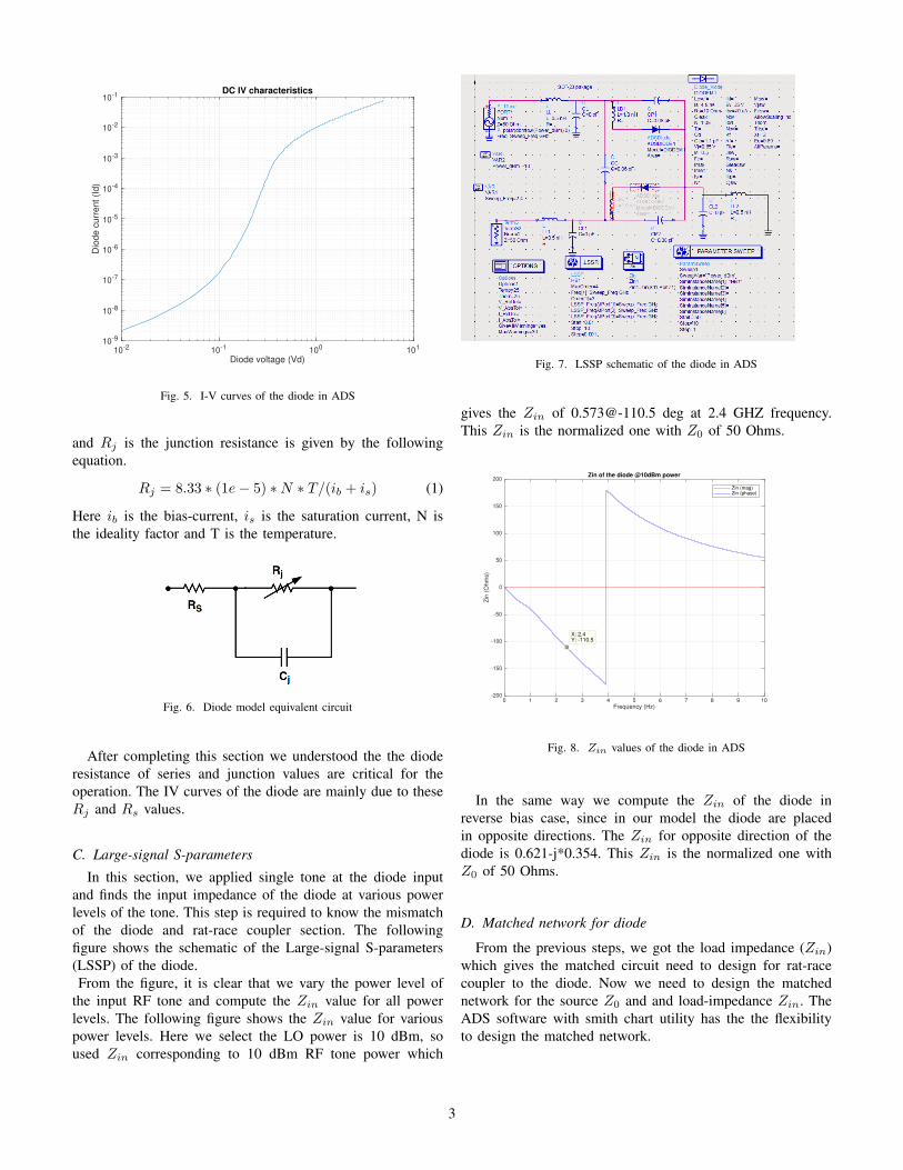
B. I-V characteristics
In this section, we performed the DC-simulation of thediode which mainly says the IV characteristics of the diode.The given ADS template have this step which plots the I-Vcharacteristics. The following figure shows the dc-simulationsetup of the diode using ADS.
Fig. 4. DC simulation of diode in ADS
The following figure shows the IV characteristics of the diodefrom ADS. The IV curves dives into the 3- regions, first oneis the saturation current below vD of the diode where as thesecond one the diode current is dominated by input voltagefrom the effect of junction resistance (Rj) and the third oneis diode current by linear voltage by the Resistance (Rs).These characteristics can be seen in log-log plot of IV curves.The diode has series resistance (Rs) of 10 ohms.
The diode equivalent linear model is shown below.Here theRs is the series resistance, Cj is the junction capacitance
2
10-2 10-1 100 101
Diode voltage (Vd)
10-9
10-8
10-7
10-6
10-5
10-4
10-3
10-2
10-1D
iode c
urr
ent (I
d)
DC IV characteristics
Fig. 5. I-V curves of the diode in ADS
and Rj is the junction resistance is given by the followingequation.
Rj = 8.33 ∗ (1e− 5) ∗N ∗ T/(ib + is) (1)
Here ib is the bias-current, is is the saturation current, N isthe ideality factor and T is the temperature.
Fig. 6. Diode model equivalent circuit
After completing this section we understood the the dioderesistance of series and junction values are critical for theoperation. The IV curves of the diode are mainly due to theseRj and Rs values.
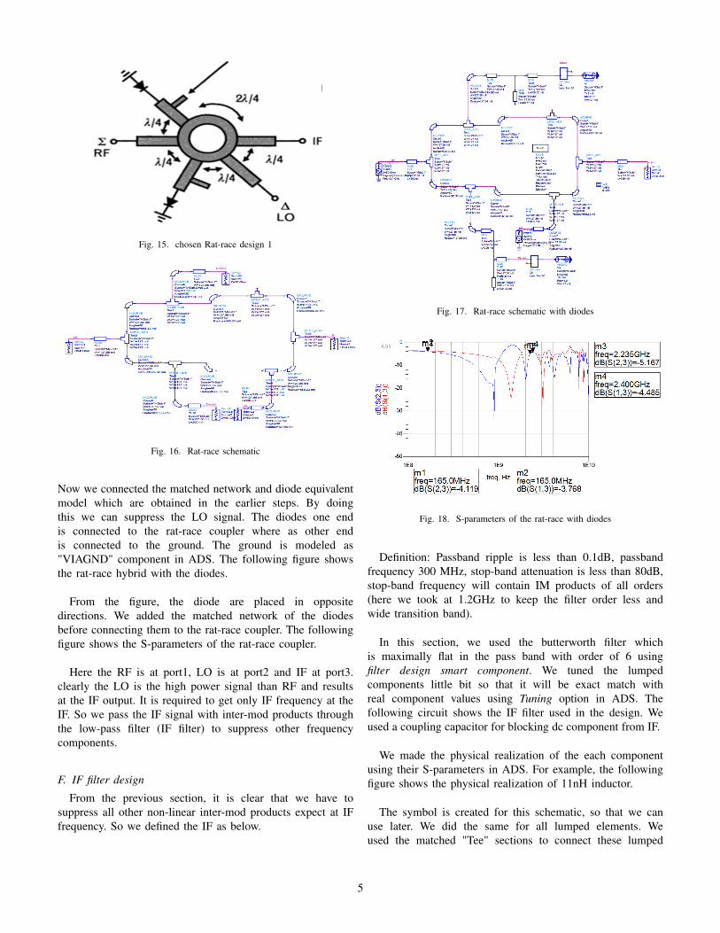
C. Large-signal S-parameters
In this section, we applied single tone at the diode inputand finds the input impedance of the diode at various powerlevels of the tone. This step is required to know the mismatchof the diode and rat-race coupler section. The followingfigure shows the schematic of the Large-signal S-parameters(LSSP) of the diode.From the figure, it is clear that we vary the power level of
the input RF tone and compute the Zin value for all powerlevels. The following figure shows the Zin value for variouspower levels. Here we select the LO power is 10 dBm, soused Zin corresponding to 10 dBm RF tone power which
Fig. 7. LSSP schematic of the diode in ADS
gives the Zin of [email protected] deg at 2.4 GHZ frequency.This Zin is the normalized one with Z0 of 50 Ohms.
0 1 2 3 4 5 6 7 8 9 10Frequency (Hz)
-200
-150
-100
-50
0
50
100
150
200
Zin
(O
hm
s)
Zin of the diode @10dBm power
Zin (mag)Zin (phase)
X: 2.4Y: -110.5
Fig. 8. Zin values of the diode in ADS
In the same way we compute the Zin of the diode inreverse bias case, since in our model the diode are placedin opposite directions. The Zin for opposite direction of thediode is 0.621-j*0.354. This Zin is the normalized one withZ0 of 50 Ohms.
D. Matched network for diode
From the previous steps, we got the load impedance (Zin)which gives the matched circuit need to design for rat-racecoupler to the diode. Now we need to design the matchednetwork for the source Z0 and and load-impedance Zin. TheADS software with smith chart utility has the the flexibilityto design the matched network.
3
In this step, we designed load-impedance matched networkfor diode in forward bias. The load-impedance is 19.3-j*31.5ohms. The following figure shows the load-matched network.
Fig. 9. Load-matching network from smith chart tool
Using the Smith Chart Utility, we got the schematics withequivalent electrical lengths. By using the Line-cal toolin ADS, we got the equivalent physical length of thetransmission lines. We used open stubs which is easy todesign, since these don’t need to connect to via.
Fig. 10. Load-matching network with stub physical length
The Line-Cal tool gives us the length and width ofthe transmission lines for the specified impedance andTransmission lines length. In the same way, we computed theelectrical and physical lengths of the diode matched networkin reverse bias. The following figure shows the matchingnetwork for diode in opposite direction.
Fig. 11. Load-matching network for reverse direction of diode
The following figure shows the equivalent physical lengths ofthe matched network.Till this section, we finished the diode model and matchednetwork of the diode.
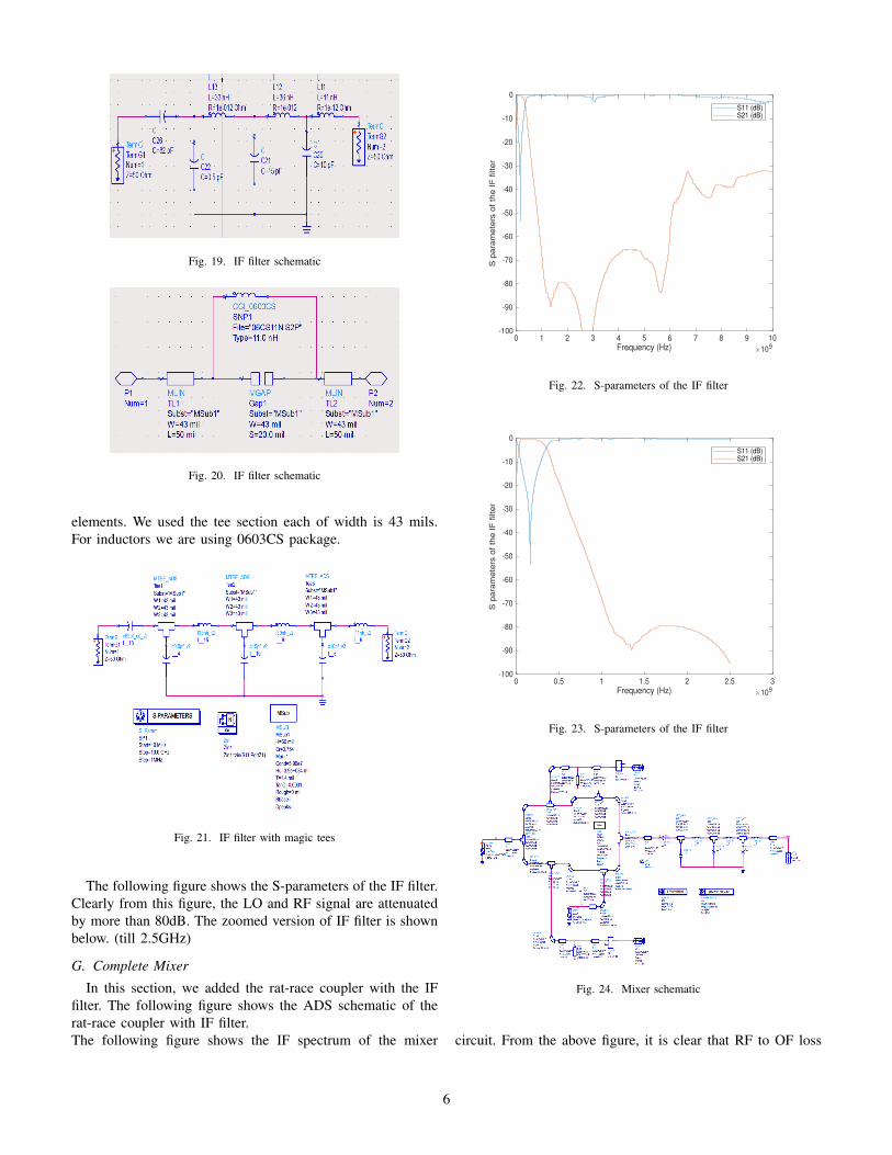
E. Rat-race Coupler
The important component in the mixer design is the hybridof 90 deg or 180 deg. Here we are using 180 deg hybrid
Fig. 12. Load-matching network with physical length for reverse directionof diode
which is the rat-race coupler. The rat-race coupler is havinglength of 1.5*λ of length. Out of which 3 ports are separatedby λ/4 and other one is separated by three times λ/4. Thefollowing figure shows the general rat-race coupler design.From the figure, the port P1 is the RF input, port P2 is the
Fig. 13. Rat-race coupler
sum port, port P3 is the LO input and port P4 is the IF outputport. The S-parameter matrix of the rat-race coupler is givenbelow.
Fig. 14. S-matrix of the rat-race coupler
In this section, we designed the same rat-race coupler usingADS software. Design steps: Instead of λ/4 lines, we usedthe curves of the angel of 60◦. Out of the 2-designs providedby the professor we are using design 1 to make the rat-racecoupler. The following figure shows the design 1 of therat-race coupler.
As mentioned earlier, we are using curve of 60◦ with sameelectrical length instead of λ/4 lines to make the designlooks like a circle. We added another λ/4 division so thatthe diode can be placed symmetric from 3 ∗ λ/4 section. The"MCurves" are connected using matched Tee sections. Tomake the diode and LO ports vertical , we used another 30◦
curve before connecting the ports.
4
Fig. 15. chosen Rat-race design 1
Fig. 16. Rat-race schematic
Now we connected the matched network and diode equivalentmodel which are obtained in the earlier steps. By doingthis we can suppress the LO signal. The diodes one endis connected to the rat-race coupler where as other endis connected to the ground. The ground is modeled as"VIAGND" component in ADS. The following figure showsthe rat-race hybrid with the diodes.
From the figure, the diode are placed in oppositedirections. We added the matched network of the diodesbefore connecting them to the rat-race coupler. The followingfigure shows the S-parameters of the rat-race coupler.
Here the RF is at port1, LO is at port2 and IF at port3.clearly the LO is the high power signal than RF and resultsat the IF output. It is required to get only IF frequency at theIF. So we pass the IF signal with inter-mod products throughthe low-pass filter (IF filter) to suppress other frequencycomponents.
F. IF filter design
From the previous section, it is clear that we have tosuppress all other non-linear inter-mod products expect at IFfrequency. So we defined the IF as below.
Fig. 17. Rat-race schematic with diodes
Fig. 18. S-parameters of the rat-race with diodes
Definition: Passband ripple is less than 0.1dB, passbandfrequency 300 MHz, stop-band attenuation is less than 80dB,stop-band frequency will contain IM products of all orders(here we took at 1.2GHz to keep the filter order less andwide transition band).
In this section, we used the butterworth filter whichis maximally flat in the pass band with order of 6 usingfilter design smart component. We tuned the lumpedcomponents little bit so that it will be exact match withreal component values using Tuning option in ADS. Thefollowing circuit shows the IF filter used in the design. Weused a coupling capacitor for blocking dc component from IF.
We made the physical realization of the each componentusing their S-parameters in ADS. For example, the followingfigure shows the physical realization of 11nH inductor.
The symbol is created for this schematic, so that we canuse later. We did the same for all lumped elements. Weused the matched "Tee" sections to connect these lumped
5
Fig. 19. IF filter schematic
Fig. 20. IF filter schematic
elements. We used the tee section each of width is 43 mils.For inductors we are using 0603CS package.
Fig. 21. IF filter with magic tees
The following figure shows the S-parameters of the IF filter.Clearly from this figure, the LO and RF signal are attenuatedby more than 80dB. The zoomed version of IF filter is shownbelow. (till 2.5GHz)
G. Complete Mixer
In this section, we added the rat-race coupler with the IFfilter. The following figure shows the ADS schematic of therat-race coupler with IF filter.The following figure shows the IF spectrum of the mixer
0 1 2 3 4 5 6 7 8 9 10Frequency (Hz) 109
-100
-90
-80
-70
-60
-50
-40
-30
-20
-10
0
S p
ara
me
ters
of
the
IF
filte
r
S11 (dB)S21 (dB)
Fig. 22. S-parameters of the IF filter
0 0.5 1 1.5 2 2.5 3Frequency (Hz) 109
-100
-90
-80
-70
-60
-50
-40
-30
-20
-10
0
S p
ara
me
ters
of
the
IF
filte
r
S11 (dB)S21 (dB)
Fig. 23. S-parameters of the IF filter
Fig. 24. Mixer schematic
circuit. From the above figure, it is clear that RF to OF loss
6
-160
-150
-140
-130
-120
-110
-100
-90
-80
-70
-60
-50
-40
-30
-20
-10
0
Outp
ut pow
er o
f th
e IF
filte
r
0 2 4 6 8 10 12Frequency (Hz) 109
Fig. 25. Output products of the mixer circuit from Matlab
is less than 8dB, LO signal power is given by -75 dBm andRF signal at IF port is at -104 dBm.
Fig. 26. Output products of the mixer circuit from ADS
The S-parameters of the mixer circuit is given in the followingfigures.
Clearly, from the S-parameters, the conversion loss is givenby -4.43 dB which is RF to LO, RF to IF @RF frequency isgiven by -91.2 dB, the LO to IF isolation is given by -6.241dB, and the LO to RF isolation is given by -84.92 dB. Fromthis it is clear that the LO matching is not proper at the IFoutput. The matched network of the all ports are explained inthe later sections.
H. Layout design
In this section, we replace all the schematics withappropriate layout circuits. The complete layout of theschematic is shown below. The capacitors used in the designare 0.5 pF, 10 pF, 15 pF and 82 pF (coupling capacitor Cc).The inductors used in the design are 11 nH, 30 nH and 33nH. In the schematic, additional transmission line of 200 mils
0 1 2 3 4 5 6 7 8 9 10Frequency (Hz) 109
-120
-100
-80
-60
-40
-20
0
S13 o
f th
e M
ixer
S13 (dB)
Fig. 27. RF to IF S-parameters
0 1 2 3 4 5 6 7 8 9 10Frequency (Hz) 109
-80
-70
-60
-50
-40
-30
-20
-10
0
S23 o
f th
e M
ixer
LO to IF S-params
S23 (dB)
Fig. 28. LO to IF S-parameters
0 1 2 3 4 5 6 7 8 9 10Frequency (Hz) 109
-120
-100
-80
-60
-40
-20
0
S21 o
f th
e M
ixer
LO to RF S-params
S21 (dB)
Fig. 29. LO to RF S-parameters
is added to make sure we have enough transmission line toplace the ports of the transistors at all the ports. We addedviaholes for short circuit. We dig the holes for short-circuitin the design.
7
Fig. 30. Layout of the mixer circuit
III. FABRICATION
The layout using Gerber file is fabricated using the LPKFmachine. We used the Rogers 4350B substrate with effectiveresistance of 3.754, thickness is 60mil, 1oz copper (1.4mil), loss tangent of 0.0031 and conductivity of 5.96e7.We selected the appropriate settings for the milling. Thefollowing figure shows after fabrication from LPKF machine.
Fig. 31. Fabricated Mixer with LPKF machine
A. Lumped components and diodes
We soldered the capacitors, inductors and diodes on thefabricated design. We added the 3-ports for RF input, LO inputand IF output with 3.5mm SMA female connectors.
The following figure shows after adding lumped elementsand diodes.
Fig. 32. Mixer after soldering the components
IV. MEASUREMENTS
The following are the performance metrics of the mixer.1) Conversion loss: CL= Prf -Pif which is opposite of the
conversion gain (CG)2) Isolation of ports: isolation across all ports3) 1-dB compression point: impact on switching of RF
power4) Noise figure: proportional to Conversion loss5) single tone IM distortion: unwanted harmonics are called
IMD6) Multi-tone IM distortion: using 2-tone test,measure IIP3
value.Out of which here we measured the conversion loss, isolationand IIP3 values of the designed mixer. The following figureshows the typical setup for mixer measurements.
Fig. 33. Mixer measurement setup
A. Calibration
Before measuring the loss parameters, it is better tocalibrate the cables and know the cables loss. Before insertingthe Mixer in the measurement, perform the port1 and port2loss which includes the splitter. We used the Keysight vectorsignal generator(s) and signal analyzers for the measurement.
8
The loss of the splitter along with cable loss is measuredas -5.2 dB. The LO cable loss is 0.93 dB, RF cable loss is0.94 dB and IF cable loss is 0.1 dB and splitter loss is 4.16 dB.
B. Measurement setup for conversion loss
Now insert the mixer in between MXG and VSA. Weselected the RF frequency as 2.4GHz with power level of -25dBm and LO signal of 10 dBm at 2.235 GHz, which providesthe IF value of 165 MHz. we measured the IF value at 165MHz, which results as -34.4 dBm provides the conversionloss of 9.3dB. The following table gives the conversion lossat various power-levels.
RF Pin (dBm) IF Out Power (dBm)-25.1 -34.4-15.1 -24.3-5.1 -14.144.9 -4.75.9 -3.86.9 -3.157.9 -2.5
TABLE IIIF POWER VS RF PIN
The following figure shows the conversion loss vs RFpower. Here we plotted interpolated line from first RF powerto show the conversion loss in increases as the RF powerincreases which is nothing but compression at higher RFpowers. The ip1 dB is 7dBm.
-30 -25 -20 -15 -10 -5 0 5 10RF input power (dBm)
-30
-25
-20
-15
-10
-5
0
IF O
utp
ut
po
we
r
Conversion Loss (dB)
CL (dB)Ideal CL (dB)
Fig. 34. Conversion loss vs RF input power (dB)
C. Measurement setup for Isolation
In this step, we measured the isolation across all ports. TheRF to IF isolation is measured such that apply the tone atRF port and measured the tone at IF port with RF frequency.Example, apply a tone of -25.1 dBm at RF input @2.4 GHzand measure the IF @2.4 GHz (in this case, no LO signal is
applied). The RF to IF isolation is measured as 17.6 dB.
RF Pin (dBm) IF Out Power (dBm @2.4 GHz)-25.1 -47.2-15.1 -32.72
TABLE IIIRF VS IF ISOLATION
The LO to IF isolation is measured such that apply the tone atLO port and measured the tone at IF port with LO frequency.Example, apply a tone of 4.9 dBm at LO input @2.235 GHzand measure the IF @2.235 GHz (in this case, no RF signalis applied). The LO to IF isolation is measured as 20.3 dB.
In the same way, the LO to RF isolation is measuredsuch that apply the tone at LO port and measured the toneat RF port with LO frequency. Example, apply a tone of4.9 dBm at LO input @2.235 GHz and measure the RFport @2.235 GHz (in this case, IF port is terminated withmatched load). The LO to RF isolation is measured as 6.4 dB.
V. NON-LINEAR MEASUREMENTS
In this section we perform the non-linear measurementsof the designed mixer using two-tone test. In this section,we discussed mainly about the third order inter-modulationpower. The measurement setup is same as our-previous labsetup.
A. Losses measured
We measured the total loss with and without splitter.We got the loss due to each component. The splittergave the loss of 4.1 dB, the RF cable has loss of 0.94dB, LO cable has loss of 0.93 dB and IF cable has loss of0.1 dB. These losses are same in the above mentioned section.
B. IM3 vs RF power
We used a two tone (2-tone) inputs at same power levelsand measured the Pout at inter-mods using the PXA. ForRF input power, we used 2.4 GHz for generator 1 and 2.45GHz for generator 2. The inter-mod product is observed at2.5 GHz. Initially we increased the input power in steps of 5dBm, but later input power is increased in steps of 1 dBm.To find the IM3 point, the Pout at f1 and IM3 at 2f2-f1power levels should meet. We interpolated this data for morenumber of power levels.The Third-order inter-modulations curve is derived based onfew observations and interpolated throughout the Pin (dBm).The following table shows the IM3 powers vs RF inputpowers.
The following figure shows IIP3 of the mixer byinterpolating the RF input data, RF output data and IM3 data.
We observed the OP1dB and IM3 power are intersectingat input power of 23.5 dBm as IIP3 value and 14.1 dBm asOIP3 values.
VI. MATCHING OF THE MIXER
In this section, we found the match of the mixer circuitfrom all ports using ADS simulation. After the mixerdesigned, we did the S-parameters of the RF, LO and IF portsto find the refections from each of the port. The followingfigure shows the return loss of the RF port (S11).
The following figure shows the return loss of the LO port(S22).
The following figure shows the return loss of the IF port(S33).
VII. CONCLUSIONS
We designed the single balanced mixer from scratch andunderstood each component in the design which effects themixer performance. We fabricated the mixer using LPKF ma-chine with Rogers 4350B substrate with Effective permittivity
0 1 2 3 4 5 6 7 8 9 10Frequency (Hz) 109
-15
-10
-5
0
5
10
S11 o
f th
e R
F p
ort
RF port mismatch
S11 (dB)
Fig. 36. Return loss of the RF port
0 1 2 3 4 5 6 7 8 9 10
Frequency (Hz) 109
-35
-30
-25
-20
-15
-10
-5
0
5
S2
2 o
f th
e L
O p
ort
LO port mismatch
S22 (dB)
Fig. 37. Return loss of the LO port
0 1 2 3 4 5 6 7 8 9 10
Frequency (Hz) 109
-25
-20
-15
-10
-5
0
S3
3 o
f th
e I
F p
ort
IF port mismatch
S33 (dB)
Fig. 38. Return loss of the IF port
is 3.745. We performed the mixer linear and non-linear mea-surements. We understood how to measure the conversion lossof the mixer using the VSA. We verified the measured valuesare closely matching with the data sheet values. This gave us
10
confidence to design and measure any active component in thenext labs. Coming to conversion loss, we measured it which is9.3 dB. For non-linear measurements, we used two-tone tests,same as with our previous labs. The compression point andIM3 points are measured and verified using data sheets, herethe IIP3 is 17.9 dBm.
REFERENCES
[1] HSMS-281x datasheet.pdf.[2] Avago Technologies Application Note 1124.pdf.[3] Class notes and material provided by Professor[4] Johnson Technologies Capacitors (JTI0603SseriesCAPS 2011)
datasheet.pdf[5] Coilraft (CCI) RF Library (0603CS inductors) datasheet.pdf[6] Asif Ahmed. A Study and Design of a Rat-Race Coupler Based
Microwave Mixer. Journal of Electrical and Electronic Engineering. Vol.3, No. 5, 2015, pp. 121-126. doi: 10.11648/j.jeee.20150305.14