UNIVERSITY OF ENGINEERING AND TECHNOLOGY, TAXILA FACULTY OF TELECOMMUNICATION AND INFORMATION ENGINEERING DEPARTMENT OF COMPUTER ENGINEERING Digital Logic Design Lab Instructor:-Engr. Aamir Arsalan Session:-2K15 Computer Digital Logic Design Design of Binary Adder and its Verilog Coding Student Name: Registration No: ____________________________ Instructor Signature: ___________________________ Dated: 18 th April, 2016 to 22 ndApril, 2016 Semester:Spring 2016
FACULTY OF TELECOMMUNICATION AND INFORMATION ENGINEERING
DEPARTMENT OF COMPUTER ENGINEERING
Digital Logic Design Lab Instructor:-Engr. Aamir Arsalan
Session:-2K15 Computer
Objective:-
The Objectives of this lab is to understand:
1. The design and working of binary adders.
2. Implement the design in Proteus.
3. Write the code in Verilog and verify it.
Theory:-
Digital computers perform a variety of information-processing tasks. Among the functions
encountered are the various arithmetic operations. The most basic arithmetic operation is the
addition of two binary digits. This simple addition consists of four possible elementary operations:
0 + 0 = 0, 0 + 1 = 1, 1 + 0 = 1, and 1 + 1 = 10. The first three operations produce a sum of one
digit, but when both augend and addend bits are equal to 1, the binary sum consists of two digits.
The higher significant bit of this result is called a carry. When the augend and addend numbers
contain more significant digits, the carry obtained from the addition of two bits is added to the next
higher order pair of significant bits. A combinational circuit that performs the addition of two bits
is called a half adder. One that performs the addition of three bits (two significant bits and a
previous carry) is a full adder. The names of the circuits stem from the fact that two half adders
can be employed to implement a full adder.
A binary adder – subtractor is a combinational circuit that performs the arithmetic operations of
addition and subtraction with binary numbers. We will develop this circuit by means of a
hierarchical design. The half adder design is carried out first, from which we develop the full adder.
Connecting n full adders in cascade produces a binary adder for two n -bit numbers. The
subtraction circuit is included in a complementing circuit.
Half Adder:-
From the verbal explanation of a half adder, we find that this circuit needs two binary inputs and
two binary outputs. The input variables designate the augend and addend bits; the output variables
produce the sum and carry. We assign symbols x and y to the two inputs and S (for sum) and C
(for carry) to the outputs. The truth table for the half adder is listed in table given below. The Coutput is 1 only when both inputs are 1. The S output represents the least significant bit of the sum.
FACULTY OF TELECOMMUNICATION AND INFORMATION ENGINEERING
DEPARTMENT OF COMPUTER ENGINEERING
Digital Logic Design Lab Instructor:-Engr. Aamir Arsalan
Session:-2K15 Computer
Full Adder:-
Addition of n-bit binary numbers requires the use of a full adder, and the process of addition
proceeds on a bit-by-bit basis, right to left, beginning with the least significant bit. After the least
significant bit, addition at each position adds not only the respective bits of the words, but must
also consider a possible carry bit from addition at the previous position. A full adder is a
combinational circuit that forms the arithmetic sum of three bits. It consists of three inputs and two
outputs. Two of the input variables, denoted by x and y, represent the two significant bits to be
added. The third input, z, represents the carry from the previous lower significant position. Two
outputs are necessary because the arithmetic sum of three binary digits ranges in value from 0 to
3, and binary representation of 2 or 3 needs two bits. The two outputs are designated by the symbols
S for sum and C for carry. The binary variable S gives the value of the least significant bit of thesum. The binary variable C gives the output carry formed by adding the input carry and the bits of
the words. The truth table of the full adder is listed in table given below.
The eight rows under the input variables designate all possible combinations of the three variables.
The output variables are determined from the arithmetic sum of the input bits. When all input bits
are 0, the output is 0. The S output is equal to 1 when only one input is equal to 1 or when all three
inputs are equal to 1. The C output has a carry of 1 if two or three inputs are equal to 1.
FACULTY OF TELECOMMUNICATION AND INFORMATION ENGINEERING
DEPARTMENT OF COMPUTER ENGINEERING
Digital Logic Design Lab Instructor:-Engr. Aamir Arsalan
Session:-2K15 Computer
The S output from the second half adder is the exclusive-OR of z and the output of the first half
adder, giving
= ⨁(⨁)
= ( ) ( ′)′
= ( ) ( ′′)
= ′
The carry output is
= ( ) =
Binary Adder:-
A binary adder is a digital circuit that produces the arithmetic sum of two binary numbers. It can
be constructed with full adders connected in cascade, with the output carry from each full adder
connected to the input carry of the next full adder in the chain.
Addition of n-bit numbers requires a chain of n full adders or a chain of one-half adder and n-1
full adders. In the former case, the input carry to the least significant position is fixed at 0. Figure
below shows the interconnection of four full-adder (FA) circuits to provide a four-bit binary ripplecarry adder. The augend bits of A and the addend bits of B are designated by subscript numbers
from right to left, with subscript 0 denoting the least significant bit. The carries are connected in a
chain through the full adders. The input carry to the adder is C0, and it ripples through the full
adders to the output carry C4. The S outputs generate the required sum bits. An n -bit adder requires
n full adders, with each output carry connected to the input carry of the next higher order full adder.
FACULTY OF TELECOMMUNICATION AND INFORMATION ENGINEERING
DEPARTMENT OF COMPUTER ENGINEERING
Digital Logic Design Lab Instructor:-Engr. Aamir Arsalan
Session:-2K15 Computer
Carry Look Ahead Generator:-
The addition of two binary numbers in parallel implies that all the bits of the augend and addend
are available for computation at the same time. As in any combinational circuit, the signal must
propagate through the gates before the correct output sum is available in the output terminals. The
total propagation time is equal to the propagation delay of a typical gate, times the number of gate
levels in the circuit. The longest propagation delay time in an adder is the time it takes the carry to
propagate through the full adders. Since each bit of the sum output depends on the value of the
input carry, the value of Si at any given stage in the adder will be in its steady-state final value
only after the input carry to that stage has been propagated. In this regard, consider output S3 in
figure of full adder shown above. Inputs A3 and B3 are available as soon as input signals are applied
to the adder. However, input carry C3 does not settle to its final value until C2 is available from the previous stage. Similarly, C2 has to wait for C1 and so on down to C0. Thus, only after the carry
propagates and ripples through all stages will the last output S3 and carry C4 settle to their final
correct value.
The number of gate levels for the carry propagation can be found from the circuit of the full adder.
The circuit is redrawn with different labels shown in figure below for convenience. The input and
output variables use the subscript i to denote a typical stage of the adder. The signals at P i and Gi
settle to their steady-state values after they propagate through their respective gates. These two
signals are common to all half adders and depend on only the input augend and addend bits. The
signal from the input carry Ci to the output carry Ci+1 propagates through an AND gate and an ORgate, which constitute two gate levels. If there are four full adders in the adder, the output carry
C4 would have 2 * 4 = 8 gate levels from C0 to C4. For an n -bit adder, there are 2n gate levels for
the carry to propagate from input to output.
The carry propagation time is an important attribute of the adder because it limits the speed with
which two numbers are added. Although the adder or for that matter, any combinational circuit —
will always have some value at its output terminals, the outputs will not be correct unless the
signals are given enough time to propagate through the gates connected from the inputs to the
outputs. Since all other arithmetic operations are implemented by successive additions, the time
consumed during the addition process is critical. An obvious solution for reducing the carry propagation delay time is to employ faster gates with reduced delays. However, physical circuits
have a limit to their capability. Another solution is to increase the complexity of the equipment in
such a way that the carry delay time is reduced. There are several techniques for reducing the carry
propagation time in a parallel adder. The most widely used technique employs the principle of
FACULTY OF TELECOMMUNICATION AND INFORMATION ENGINEERING
DEPARTMENT OF COMPUTER ENGINEERING
Digital Logic Design Lab Instructor:-Engr. Aamir Arsalan
Session:-2K15 Computer
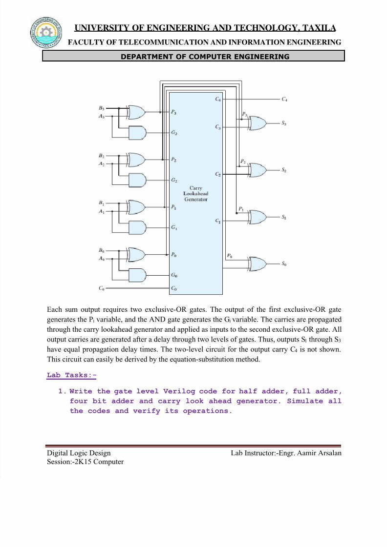
Logic diagram of carry lookahead generator
Note that this circuit can add in less time because C3 does not have to wait for C2 and C1 to propagate; in fact, C3 is propagated at the same time as C1 and C2. This gain in speed of operation
is achieved at the expense of additional complexity (hardware).
The construction of a four-bit adder with a carry lookahead scheme is shown in figure below.


![[HCI Lab] Week 06 Prototyping](https://static.documents.pub/doc/80x56/55a6227d1a28abf0278b4654/hci-lab-week-06-prototyping.jpg)


