Laboratory #2 Design and Understanding of RF Components: Inductors & Varactors Objectives: To learn the fundamentals of inductors and varactors for RF CMOS circuits, to learn the design and characterization of inductors and varactors and to understand the use of ASITIC for the simulation of inductors implemented in silicon technologies. 1. VARACTORS 1.1 Explain different types of varactors that are employed in RF CMOS design, and discuss the pros and cons of each. What is the most common use of varactors in RFIC design? Evaluate each different type of varactor and their pros and cons with respect to this common application. One crucial variable of both receiving and transmitting blocks is the tuning of LC oscillators. These are typically implemented by monolithic inductors. Since inductors are difficult to be varied the only freedom in the oscillation frequency is the value of the capacitance. In this sense, a lot of variable (voltage dependent) capacitors are utilized in monolithic LC oscillators and are called varactors. Fig. 1 Reversed bias PN junction One type of varactor is the reverse biased P-N junction, shown in Fig. 1. The voltage dependent capacitance can be expressed as the following.
Transcript
Laboratory #2Design and Understanding of RF Components: Inductors & Varactors
Objectives: To learn the fundamentals of inductors and varactors for RF CMOS circuits, to learn the design and characterization of inductors and varactors and to understand the use of ASITIC for the simulation of inductors implemented in silicon technologies.
1. VARACTORS1.1 Explain different types of varactors that are employed in RF CMOS design, and discuss the pros and cons of each. What is the most common use of varactors in RFIC design? Evaluate each different type of varactor and their pros and cons with respect to this common application.
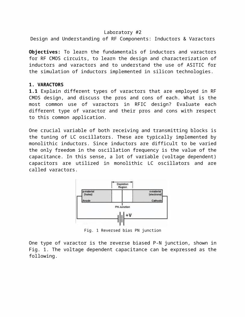
One crucial variable of both receiving and transmitting blocks is the tuning of LC oscillators. These are typically implemented by monolithic inductors. Since inductors are difficult to be varied the only freedom in the oscillation frequency is the value of the capacitance. In this sense, a lot of variable (voltage dependent) capacitors are utilized in monolithic LC oscillators and are called varactors.
Fig. 1 Reversed bias PN junction
One type of varactor is the reverse biased P-N junction, shown in Fig. 1. The voltage dependent capacitance can be expressed as the following.
C var=Co
(1+ VV a
)n
It is evident from the equation that the tuning range of P-N junction varactor is reduced with lower supply voltage. To maximize the tuning range, the absolute value of varactor should be minimized but the parasitic capacitances prevents from using small values of capacitance. One can also notice that the P-N junction varactor shows non-symmetric capacitor variation, thereby introducing significant nonlinearity. At lower supply voltage, it is more difficult to select the proper biasing point where the junction is not to be forward biased.
The second type of varactor is the one implemented with MOSFET devices. If the source and drain are shorted the device can serve as a variable capacitor as well. However, a large resistance between source and drain makes the Q of varactor low and this is a serious shortcoming for the
use of MOSFET as a varactor for RF applications. To overcome this problem the accumulation mode MOSFET is mostly used in the tuning of the oscillating frequency. This varactor can work with both positive and negative voltages and provide maximum dynamic range. Accumulation mode varactors have n+ diffusions in an n-well, rather than in a p-type region. The capacitance is high when a positive voltage is applied to the gate, attracting electrons under the gate and forming an accumulation region. MOS varactors generally offer higher Q, since there are fewer parasitic junctions and paths to ground. However, they cannot be modeled as a standard MOSFET with the drain and source tied together; instead a custom model must be used. MOS varactors can be used to operate in inversion, depletion or accumulation mode.
Fig. 2 Accumulation Mode MOSFET
1.2 Use a PMOS transistor (W= 12 x 15µm , L=1.2µm) to create a varactor. What type of varactor is this? Obtain the Capacitance vs. Vgs plots of this varactor at 1GHz, 1.9GHz and 2.4GHz. Show your simulation setup and include a detailed explanation of how you obtained these characterization plots. (Hint: Use the “family” and “value” functions of Cadence)
Fig. 3 shows the simulation setup used in Cadence for the extraction of the voltage dependent capacitance for a PMOS.
Fig. 3 Setup for capacitance simulation
From the Ohm’s Law we can get to the following formula for the capacitance:
C= If
Where it has been assumed that the voltage applied is unity. Fig. 4 shows the voltage dependent capacitance for three different frequencies and Fig. 5 shows the simulation parameters used in Cadence.
Fig. 4 Voltage dependent capacitance for a PMOS
Fig. 5 Simulation setup
2. INDUCTORS
2.2 Explain the impact of inductor design parameters (metal layer, radius, metal width, etc.) on the inductor performance (inductance, quality factor, parasitics, etc.). Discuss the non-idealities and loss mechanisms in a monolithic inductor. Discuss why in new RF CMOS processes there is a dedicated metal layer for inductors? What are the main distinguishing characteristics of this metal layer?
By using standard IC processes it is possible to design on-chip inductors. Most of the designs are based in the geometric shapes shown in Fig. 6. In order to use this shapes the technology needs to have at least two metal layers since the inner connection cannot use the same metal to be connected with another component.
Fig. 6 Monolithic inductor shapes
Nevertheless, the trade-offs presented on the design of integrated inductors are significant. First, the amount of noise, distortion and power consumption is higher than the off-chip inductors. Furthermore, because of the type of geometries permitted by most layout tools, circular spirals can’t be implemented and this limits the quality factor that one can get from on-chip inductors. Another limitation while working with integrated inductors is the area needed to achieve values larger than a few tens of nH. Therefore, practical on-chip inductances are on the order of 10nH.Fig. 7 shows a cross-section of an integrated spiral inductor. The magnetic field B(t) produces two effects: self and mutual inductance coupling among the metal tracks composing the inductor and current induced in the substrate and metal tracks. The electric field E 1(t), results of the voltage difference between the two ends of the spiral and produces ohmic losses due to the resistivity of the metal tracks. The electric field E2(t), is generated from the voltage difference between adjacent strips and between those and the inner connections. They produce capacitive coupling among the coils of the inductor. The electric field E3(t), is generated as a result of the existing voltage difference between the spiral and the substrate. It produces capacitive coupling between the spiral and substrate and ohmic losses in the conductor substrate due to displacement currents induced through the capacitive coupling between the spiral and substrate.
Fig. 7 Cross-section view of a monolithic inductor
Most of the DC resistive losses are worsened by the skin effect, which causes the current to flow in the borders of the metal tracks. This can be seen as the alteration of the current density distribution from the magnetic field generated by the current itself. As shown in Fig. 8, when a magnetic field generated by a current in a conductor crosses its cross-section, it induces a force over the current itself. This force is perpendicular to the magnetic field and to the direction of the
current flow. Then, the current is pushed toward the outer surface of the conductor. This increases the effective series resistance seen on spiral inductors.
Fig. 8 Skin effect in a rectangular conductor
In the same way, there are parasitic capacitances between the metal traces and the substrate that will resonate with the inductor. The resonance frequency is the higher upper frequency of the inductor and is often low, which makes the inductor useless in most of the cases. Also, because of the proximity to the substrate, energy is coupled into it resulting on a degradation of the quality factor. In order to understand the way in which the parasitic elements discussed before affect the inductor’s performance a circuit model needs to be used. A common model used for integrated inductors is the model known as the “pi” model and is shown in Fig. 9.
Fig. 9 “PI” model for integrated inductors
CP represents the capacitance among the strips and between the strips and the coil inner connection, usually this capacitance is negligible. RS represents the inductor resistance, which accounts for the ohmic losses due to the metal track resistance, induced electric fields on the
metallic conductor and magnetic induced currents in the substrate. LS model the actual inductance of the coil. COX represents the parasitic capacitance between the metal of the spiral and the substrate. RSI represents the ohmic losses in the substrate produced by the displacement currents induced in the substrate. CSI models the capacitive effects of the substrate due to its semiconductor characteristics. A drawback of this model is that many of its components, like resistance, inductance, substrate parasites, depend on frequency. Because of this, the model is valid for a small range of frequencies (from 0.2 GHz to 1GHz), or when losses on the substrate are negligible. The following equations are used to compute each of the parameters of the model as a function of the inductor geometric values and fabrication process parameters. First we have the inductor resistance RS.
Where w is the width and t the depth of the strip, l is the length of the spiral, δ the skin depth at the considered frequency and ρ the resistivity of the metal. The inductance LS is computed using the H.M. Greeenhouse algorithm presented in [1]. The capacitances showed on the model are computed using the next equations:
Where n is the number of crossings between the coil and the central lower connection, εOX is the oxide dielectric constant, toxM1-M2 is the oxide depth between the spiral tracks and its central interconnection.
Where Csub and Gsub are the substrate capacitance and conductance per unit area, respectively. These two constants are empirically computed.An important remark is that the above expressions allow a qualitative rather than a quantitative analysis of the inductor, since there are limitations in the validity of some of the equations. Other drawback is that the proposed expression for the computation of the resistance is more appropriate for circular conductors rather than rectangular. Finally, this model is only valid when none of the two ports of the inductor is connected to AC ground. When this is not the case, the model is simpler and is called the one-port Pi model. This simplified model is shown in Fig. 10.
Fig. 10 One-port “Pi” model for integrated inductors
In order to improve the quality factor of integrated inductors, newer technologies use thick metal processes and high resistive substrate. The high resistive substrate helps to reduce the substrate loss of spiral inductor due to the conducting substrate. Furthermore, thick metal process helps to reduce the resistance of the inductors, therefore minimizing the losses due to Rs. The next table shows a comparison of inductors fabricated using different substrate resistances and metal thicknesses [2].
Table 1: Several inductors fabricated with different substrate resistances and metal thickness.
In conclusion, to achieve higher quality factors, the use of high resistive substrate and thick metal layers is needed to decrease parasitic resistances and therefore increase the value of Q.
2.3 Following the sample session, design 10 different inductors (with different shapes, sizes and dimensions for the metal lines). The aim of this exercise is to see the realistic inductor values in this technology (i.e. maximum Q you can achieve with realistic inductance values, etc.) and have an idea of the area it will cost you.Make a table to show the design parameters you picked for each inductor, include the inductance and quality factor at 1.9GHz (use “pix” command to monitor this). Discuss your observations.(Some sample dimensions can be taken from: S. S. Mohan, et. Al., “Simple Accurate Expressions for Planar Spiral Inductances”, IEEE Journal of Solid-State, Vol. 34, No. 10, October 1999.)
3.1 Pick three of the inductors you designed in section 2.3 and check the pi model and quality factor of the inductor at several different frequencies using the pix command to obtain a plot of Q vs. Frequency. (Note that for a given geometry, inductance will slightly change at different frequencies, as long as this change is small, you can ignore it.). What is the qualitative explanation behind the shape of the Q vs.f curve, what effects are dominant in different parts of this plot?
Command used: 2portx L3 0.1 4 0.1 PI rect fast <filename> L3
Quality Factor vs. InductanceThe behavior of the Q factor with respect to the inductance value is of particular interest in RF design. In this section we will obtain Q vs. L curves by changing the geometric properties of inductors.
3.2 Obtain Q vs. L plots as shown in the figures. Pick a sweep parameter to obtain a plot similar to Figure 1. Perform the pi model analysis for your inductors at three different frequencies to obtain three plots.
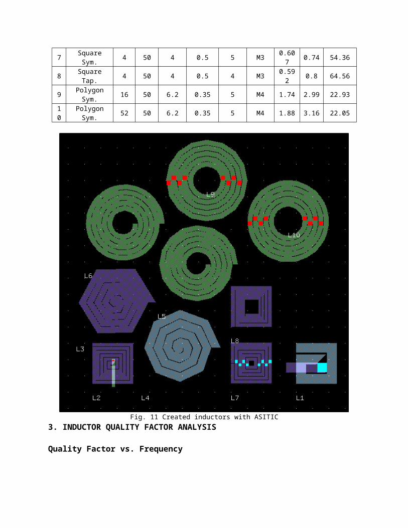
Fig. 12 Created inductors with ASITIC
Inductor Quality Factor OptimizationAs we saw from section 3.2, for certain frequencies or inductor ranges, Q decreases with increasing inductance value.Let’s take an inductor L1 with Q1 = ωL1 / R1. Theoretically, if we add two of these inductors in series we will have equivalent inductance Leq = 2L1 but the effective Q will be Qeq = Q1. However, we have seen that under certain conditions Q decreases for increasing inductance for a single inductor. Then, we could form large inductors from series combination of smaller inductors and therefore obtain a better Q than we would have by using one large inductor.
3.3 Is the above statement true? Please clearly state your answer. Support your answer with theoretical physical reasoning and ASITIC examples. You can use “join” command to perform series addition of inductors. (For any inductor you use in your explanation, give the values of all the geometry parameters for that inductor as well as the pi model results for a particular frequency. Make sure that you are doing a fair comparison between inductors.)
Yes the statement is true. The reason is that the mutual inductance between each inductor is not been considered usually when the inductors are added in series. If we consider the effects of adding
inductors in series and the mutual inductance between each other the total inductance will be higher than just adding each inductor in series hence giving a higher Q value.
First we have one inductor of Radius: 90 um, Width: 6 um, Spacing: 0.6um, N: 6, Metal layer: M4, Sides: 16 at 1.9 GHz. After the extracting the parameters with the pix command we got the following:
Inductance = 5.68 nHQ = 2.38, 2.11, 2.91
Then we created for inductors with the following parameters. Radius: 50 um, Width: 6 um, Spacing: 0.6um, N: 6, Metal layer: M4, Sides: 16 at 1.9 GHz. After the extracting the parameters with the pix command we got the following:
Inductance = 5.71 nHQ = 2.45, 2.41, 2.56
Fig. 13 Created inductors with ASITIC
References[1] T.H. Lee, “The Design of CMOS Radio-Frequency Integrated Circuits”, Cambridge University Press, Cambridge, UK. 2002.[2] C.S. Kim, et.al. “Thick Metal CMOS Technology on High resistivity Substrate and Its Application to Monolithic L-Band CMOS LNAs”, ETRI Journal, Vol. 21. No. 4, Dec 1999.