“Proceedings of the 2003 American Society for Engineering Education Annual Conference & Exposition Copyright 2003, American Society for Engineering Education” Session 1526 LABORATORY EXPERIMENTS UNIFYING CONCEPTS IN THE COMMUNICATIONS, DIGITAL SIGNAL PROCESSING (DSP) AND VERY LARGE SCALE INTEGRATION (VLSI) COURSES Ravi P. Ramachandran, Linda M. Head, Shreekanth A. Mandayam, John L. Schmalzel and Steven H. Chin Department of Electrical and Computer Engineering, Rowan University, Glassboro, New Jersey 08028 Abstract - The hallmark of the Rowan College of Engineering undergraduate program is to provide effective laboratory based instruction that illustrates important scientific concepts. This paper presents the results of an effort by the Department of Electrical and Computer Engineering at Rowan University to configure a novel method of teaching the junior level Communications (COMM), Digital Signal Processing (DSP) and Very Large Scale Integration (VLSI) courses under a common laboratory framework. These three courses are taken concurrently during the spring semester of the junior year. The described interdisciplinary experiments cut across individual course boundaries and integrate hands-on experience and software simulation. Software is integrated with the experiments through MATLAB and SIMULINK, C/C++ and Mentor Graphics. Introduction This project is an effort by the Department of Electrical and Computer Engineering at Rowan University to configure a novel method of teaching the junior level Communications (COMM), Digital Signal Processing (DSP) and Very Large Scale Integration (VLSI) courses under a common framework. These three courses are taken concurrently during the spring semester of the junior year. The effort is aimed at establishing a “proof of concept”. There has been a historical division and separation of the fields of Communications, DSP and VLSI in electrical engineering education. This separation has crept up to the very high professional circles in both industry and university. Engineers specialized in one area find it hard to collaborate with their colleagues and separate cliques within the department start to form. This
Transcript
“Proceedings of the 2003 American Society for Engineering Education Annual Conference & Exposition Copyright 2003, American Society for Engineering Education”
Session 1526
LABORATORY EXPERIMENTS UNIFYING CONCEPTS IN THE COMMUNICATIONS, DIGITAL SIGNAL PROCESSING (DSP) AND
VERY LARGE SCALE INTEGRATION (VLSI) COURSES
Ravi P. Ramachandran, Linda M. Head, Shreekanth A. Mandayam, John L. Schmalzel and Steven H. Chin
Department of Electrical and Computer Engineering, Rowan University, Glassboro, New Jersey 08028
Abstract - The hallmark of the Rowan College of Engineering undergraduate program is to
provide effective laboratory based instruction that illustrates important scientific concepts. This
paper presents the results of an effort by the Department of Electrical and Computer Engineering
at Rowan University to configure a novel method of teaching the junior level Communications
(COMM), Digital Signal Processing (DSP) and Very Large Scale Integration (VLSI) courses
under a common laboratory framework. These three courses are taken concurrently during the
spring semester of the junior year. The described interdisciplinary experiments cut across
individual course boundaries and integrate hands-on experience and software simulation.
Software is integrated with the experiments through MATLAB and SIMULINK, C/C++ and
Mentor Graphics.
Introduction
This project is an effort by the Department of Electrical and Computer Engineering at
Rowan University to configure a novel method of teaching the junior level Communications
(COMM), Digital Signal Processing (DSP) and Very Large Scale Integration (VLSI) courses
under a common framework. These three courses are taken concurrently during the spring
semester of the junior year. The effort is aimed at establishing a “proof of concept”.
There has been a historical division and separation of the fields of Communications, DSP
and VLSI in electrical engineering education. This separation has crept up to the very high
professional circles in both industry and university. Engineers specialized in one area find it hard
to collaborate with their colleagues and separate cliques within the department start to form. This
“Proceedings of the 2003 American Society for Engineering Education Annual Conference & Exposition Copyright 2003, American Society for Engineering Education”
type of segregation is no longer acceptable as we must provide an integrative experience at the
undergraduate level.
Rowan University began as a teacher education institution. It then evolved into a
comprehensive state college and now into a university. The School of Engineering is a recent
expansion for the college; a major gift in 1992 from the Rowan Foundation was the catalyst for
adding engineering. Our new engineering programs seek to use innovative methods of teaching
and learning to better prepare students for entry into a rapidly changing and highly competitive
marketplace. Key program features include: (1) an analytical and hands-on balance created
through collaborative laboratory and lecture material; (2) an emphasis on teamwork as the
necessary framework for solving complex problems; (3) incorporation of appropriate
technologies throughout the curricula; and (4) creation of continuous opportunities for technical
communication. To best meet these objectives, our programs include a multidisciplinary
engineering clinic every semester [1][2][3]. Sharing many features in common with the model
for medical training, the clinic provides an atmosphere of faculty mentoring in a hands-on,
laboratory setting. In addition to the clinic, specialized courses are taught to deliver a well
blended combination of theoretical and practical skills. This project is in accordance with the
aims of our new programs and strives to meet the requirements of industry in hiring engineers
who can move across rather artificial course boundaries with great ease.
The common educational framework we envision will enable the students to better
comprehend the conceptual relationships of COMM, DSP and VLSI. Implementation of our
ideas is facilitated by the fact that the three courses are run in the same semester. Each course has
three hours of lectures and three hours of laboratory per week. The illustrative laboratory
experiences enforce the conceptual relationships. This philosophy is further motivated by the
need to promote the two main learning styles that students have [4]. Most students, instructors
and curricula are sequential in that the process functions with partial understanding, there is
steady progress, and details are emphasized [4]. Global learners need the big and overall picture
for proper comprehension and progress in leaps despite being slow initially [4]. The present
implementation of our curriculum caters extremely well to the majority of students that adopt
sequential learning. However, stressing the common framework and thereby the big picture that
envelopes COMM, DSP and VLSI accomplishes the very important need of addressing the
“Proceedings of the 2003 American Society for Engineering Education Annual Conference & Exposition Copyright 2003, American Society for Engineering Education”
minority of global learners who would otherwise be weeded out and be a serious loss to society
[4].
Goals and Objectives
We want to accomplish the following:
1. Expose students to the different aspects and conceptual relationships among COMM,
DSP and VLSI. This will be achieved by (1) laboratory experiences that cut across the
course boundaries and (2) tuning the lecture material to stress how the fundamentals
(including the mathematical framework) envelope the material in each course.
2. Perform hardware based work that will involve VLSI architectures. The VLSI digital
circuit designs are done using complementary metal oxide semiconductor (CMOS)
technology [5].
3. Integrate software simulation with hands-on laboratory work using MATLAB, its
associated SIMULINK package, C++ programming and Mentor Graphics all of which we
have at Rowan.
4. Expand student teamwork experience by making group laboratory projects an integral
part of the course structure.
5. Continue to improve written and oral communication skills of our students.
The proposed educational material development aims to cut across traditional course
boundaries and embodies cross-platform, interdisciplinary knowledge necessary for today′s
students. The main focus is to first write a laboratory manual which describes the
interdisciplinary laboratory experiences and includes the relevant theory and conceptual
relationships linking COMM, DSP and VLSI. A long term goal is to use the laboratory manual to
write a laboratory oriented textbook. Examples of laboratory based textbooks in the DSP area
include those involving experiments with hardware boards [6][7]. However, the theoretical
background is rather brief in stressing the conceptual issues that tie DSP with COMM and VLSI.
There is one textbook that shows concepts linking DSP and COMM [8]. It is a traditional book
describing the fundamentals, mathematical background and applications but which has no
laboratory component. Here is a description of 3 experiments that will make up a part of the
laboratory manual.
Experiment 1 – Pulse Code Modulation (PCM)
“Proceedings of the 2003 American Society for Engineering Education Annual Conference & Exposition Copyright 2003, American Society for Engineering Education”
Objective
To gain a thorough understanding of Pulse Code Modulation (PCM) and about its hardware and
software implementation.
Theory
Pulse Code Modulation [9][10] is essentially analog-to-digital conversion of a special
type in which the information contained in the instantaneous samples of an analog signal is
represented by digital words. If each of the digital words used by the system contains n bits, then
there are 2n unique code words that are possible. Each of these code words represents a certain
amplitude level and the grouping of all of these code words is called a codebook. Unfortunately,
because an analog signal can be any one of an infinite number of amplitudes, it is not possible for
a digital word to represent these exact values. Instead, the system chooses the digital word that
represents the amplitude closest to the actual sample value used. This is called quantization and
it is the fundamental principle underlying PCM.
PCM is very popular in communication circuitry and bandwidth limited devices because
of the following:
• The number of bits that need to be transmitted through a medium can be greatly reduced.
• It uses relatively inexpensive circuitry.
• PCM signals that are derived from any type of analog source (audio, video, etc.) can be
merged with data signals and be transmitted over a high-speed digital communication
system.
• The noise performance of a digital system can be superior to that of an analog system.
Despite all of these advantages PCM has one noticeable disadvantage and that is that the original
signal will never be recovered once it is quantized. In most systems, this loss of precision has no
effect on the performance of the system.
There are 3 steps that are involved in creating a PCM signal. These include sampling,
quantizing and encoding. A diagram of this process follows:
“Proceedings of the 2003 American Society for Engineering Education Annual Conference & Exposition Copyright 2003, American Society for Engineering Education”
Figure 1 How to Create a PCM Signal
The first step in creating a PCM signal is to sample the original signal. In order to successfully
sample a signal, the sampling frequency must be 2 times greater than the maximum frequency
present in the original signal. This is also known as the Nyquist sampling theorem [11][12].
Next, the signal must be approximated so it matches up with one of the codebook values. This is
done by comparing the sampled value to the values in the codebook and finding the closest entry
in the codebook. This is the process that introduces error into the PCM signal and it leads to the
final step, which is encoding. The encoding process outputs a digital word (or bot stream) that
will be transmitted to a receiver. The other part of PCM occurs at the receiver end of the system.
At the receiving end, the digital word or bit stream is decoded to appropriate codebook value.
The sequence of codebook values is the quantized discrete signal analog reconstruction (digital to
analog or D/A) is performed. An example of this process follows:
“Proceedings of the 2003 American Society for Engineering Education Annual Conference & Exposition Copyright 2003, American Society for Engineering Education”
For the values –1.45, 0 and 1.60, give the codebook value and digital word that would result
from the following values. Also, determine the quantization error which is the absolute
difference between the original value and the quantized value. It is easily noticeable that the
closest value to –1.45 (see Table 1) is –1.4 and the bit stream is 0100. The error is simply 0.05V.
The closest codebook value to 0 is –0.05. The digital code word that corresponds to this value is
0111 and the error is again 0.05. The closest code book value to 1.60 is 1.75 and the
corresponding digital word is 1011. The error in choosing this value is now 0.15.
General Laboratory Description
Now that you have a general understanding of what PCM is, you are now going to
simulate a PCM system and build the components that are necessary to run a PCM system. First,
you will use C/C++ to simulate a PCM system. This lab does not require building anything and
should show you that a software implementation of PCM is relatively simple.
The final 3 parts of this lab are designed to teach you how to build the 3 main parts of a
PCM system. First, you will design a block of memory. Memory is used quite extensively
throughout the PCM system. First, it is used so that the bits coming out of the A/D converter can
be saved so that they can be compared to a codebook value. Second, it is used to store all of the
codebook values and their respective digital words. Finally, it is used to remember which values
have been eliminated when the comparison stage has begun. Although you are only going to be
required to make 1 block of memory, realize that several blocks of memory need to be used to
successfully implement a PCM system.
In the next part of this lab, you will need to implement a 4-bit full subtractor. This will
be used to measure the distance between the signal value and each codebook value. These
results will be stored in a block of memory and be used for the final phase of this PCM system,
which is the comparison phase. In the comparison phase, each of these subtracted values has an
individual bit of memory allocated for it. All of these bits start with a logic level of “1”. After
each individual comparison, the value that is further away receives a reset pulse so it is dropped
out of the comparison competition. This comparison phase continues until there is only 1
codebook value with a bit of logic ‘1’. The system then knows that this is the appropriate value
that should be sent out and the respective digital word is transmitted.
Part 1 – Software Implementation
“Proceedings of the 2003 American Society for Engineering Education Annual Conference & Exposition Copyright 2003, American Society for Engineering Education”
Objective
To achieve a software implementation of a PCM system and observe how the number of bits
used affects quantization error and hence, signal integrity.
Instructions
1. A speech signal sampled at 8 kHz will be supplied to you. Use MATLAB to convert this
signal to zero mean. Record the true standard deviation of the signal and call this the
variable G. Divide the signal by 2.5G and use this scaled signal for step 2.
2. Quantize the scaled signal using codebooks of size 4, 8 and 16 (2, 3 and 4 bits) that have
been optimized for a Laplacian input. These codebooks are used since it has been shown
that speech has a distribution function that is approximately Laplacian [10]. To perform
this step, write a C/C++ program. The codebooks will be supplied to you and can be
found in [10].
3. Multiply the quantized signals by 2.5G using MATLAB and calculate the quantization
error (using the norm function) for each of the 3 codebooks. Compare the error for the 3
codebooks and comment on your results. Listen to the 3 quantized signals (using the
soundsc function) and comment on how perceptual quality is affected by the number of
bits used.
Part 2 – Memory
Objective
To design and implement in VLSI a simple memory circuit to store values in a codebook.
Theory
Memory is one of the most important building blocks of a computer, the other two being
Input/Output and the Central Processing Unit. Memory is used to store values and instructions
that are being processed, or waiting to be processed. However, the memory within the CPU itself
is not like other memory. It is instead a collection of registers that store values and addresses of
outside memory.
This section of the lab deals with the memory needed to store the codebook values, input
streams, and calculated values. This memory does not need to be anything as extravagant as
SDRAM, or even SRAM. These types of memory would require extensive address generation,
storage and manipulation. That is beyond the scope of this lab. Instead, concentration will be
“Proceedings of the 2003 American Society for Engineering Education Annual Conference & Exposition Copyright 2003, American Society for Engineering Education”
turned to registers to store the various values needed by the PCM system to properly carry out its
function.
Registers are comprised of a very basic building block of all digital systems – the D-Flip
Flop. A D-Flip Flop allows a value to be stored within a circuit, effectively acting as a
“memory” circuit. It is made up of smaller components, with a D-Latch as the Master latch, and
an RS- or D-Latch acting as the slave. This configuration allows values to be stored within the
circuit until it is “loaded” otherwise by the clock. The truth table for a D-Flip Flop is:
D CLK Qn+
1
Qn+1*
0 0 1 0 0 1 0 1 1 0 0 1 1 1 1 0
Table 2 Truth table for a D flip-flop
What this truth table says is that when the clock pulse is high, the NEXT state of Q will be that of
the current D input. The output will follow the input as long as it is high. However, when the
clock is low, there will be no change in the next state of Q.
The D-Flip Flop is the essential component that comprises registers. One D-Flip Flop
represents a 1-bit register. However, all of the values that are to be stored in the registers are
required to be 4-bit. Also, since there are at least 16 codebook values, there needs to be a method
for selecting the correct register of the 16 used to store the values. The select must not only
allow for a read select, but also a write select.
To build a 4-bit register is a simple task. It is simply 4 1-bit registers with all of their
clocks tied together into one master clock. That way, when that register set is selected, all of the
D-Flip Flops will either write or read all at the same time.
Now that all of the clocks are tied together, there comes the task of selecting between the
registers. For example, if there were 16 registers, you would need n = log216 select bits, which
makes n = 4. Also, because of the nature of the register, loading and/or reading occur only when
the clock is high. Therefore, a circuit is required that will allow a load of that particular register
set when the clock is high. An example circuit is shown below.
“Proceedings of the 2003 American Society for Engineering Education Annual Conference & Exposition Copyright 2003, American Society for Engineering Education”
Figure 2 Circuit for CLK_In
When all 4 select bits are high, AND the Master Clock is also high, the CLK_In output will be
high. The CLK_In output acts as the clock for the registers. And thus, only when that particular
register is selected, AND the clock is high, will the register load the D values.
Now, the problem arises of reading from the correct register. Since all 16 outputs will
always be outputting a value, the outputs that are not desired must be “blocked” from reaching
the read lines. Again, the desired register for reading has 4 bits, the same 4 as that of the
selection circuit. However, the clock will not be used in this instance. Instead, a “Read” bit is
added, which performs the same function. Now, the problem arises of allowing only the selected
register to output, but keep ALL of the others blocked. An easy way to accomplish this is to use
a “Tri-State” buffer. The truth table for a Tri-State buffer is:
X Hi-Z Out
x 0 --
1 1 1
0 1 0
Table 3 Truth table for Tri-State buffer
Basically, when the Hi-Z (High Impedance) state is 0, no matter what the X input is, there
will be no output. The input is effectively blocked from passing. When the High Z state goes
high, then the input is allowed to pass through, thus allowing the selection of the desired register
for reading. An example of such a circuit is shown below:
“Proceedings of the 2003 American Society for Engineering Education Annual Conference & Exposition Copyright 2003, American Society for Engineering Education”
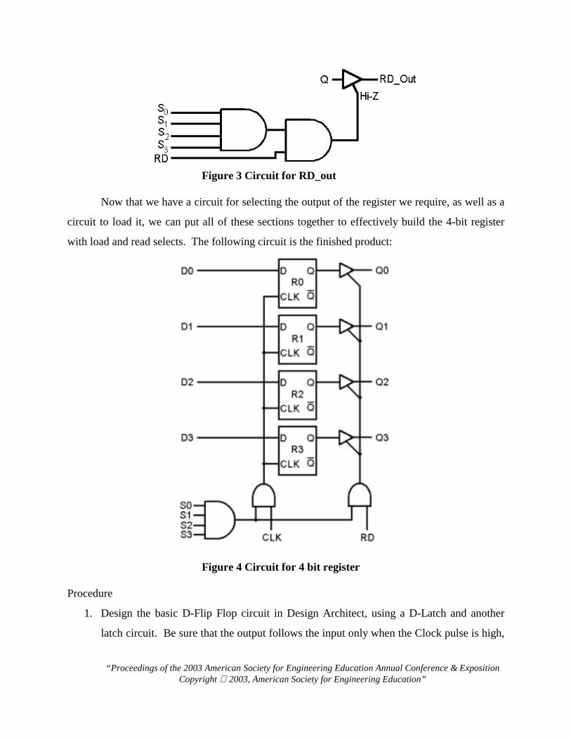
Figure 3 Circuit for RD_out
Now that we have a circuit for selecting the output of the register we require, as well as a
circuit to load it, we can put all of these sections together to effectively build the 4-bit register
with load and read selects. The following circuit is the finished product:
Figure 4 Circuit for 4 bit register
Procedure
1. Design the basic D-Flip Flop circuit in Design Architect, using a D-Latch and another
latch circuit. Be sure that the output follows the input only when the Clock pulse is high,
“Proceedings of the 2003 American Society for Engineering Education Annual Conference & Exposition Copyright 2003, American Society for Engineering Education”
and retains its value otherwise. Keep in mind the use of real estate on the DSP chip (e.g.
minimize the number of FETs).
2. Design both select circuits in Design Architect. Ensure that the tri-state buffer works
correctly for all inputs. Again, keep in mind real estate.
3. Completely simulate all circuit designs in Quicksim and Accusim. Show that the circuits
work completely.
4. Construct each circuit in IC Station. Try to keep the size of each block to a minimum.
Perform Back Annotation and Parasitic Extraction on all segments.
5. Assemble all components together into the final design of a 4-bit Register with Read and
Write select. Re-simulate in Accusim and show that the circuit works.
Questions
1. What type of latch did you use in your final D-F/F design? Why did you choose that
particular latch? How efficient is your choice in terms of FETs used?
2. When simulating your final design, did you encounter any difficulties in reading or
writing? What conflicts, if any, did you need to consider when simulating?
3. Why did we simply label each select bit S0, S1, S2, and S3 instead of specifying the select
bits to act for a specific register? What advantage does this allow?
4. Think about the overall picture for the PCM DSP chip. How many FETs do you foresee
it requiring in order to store ALL values that may need to be stored? What does this
value tell you about how and why memory is delegated within a computer (e.g. Why main
memory is external of the CPU)?
Part 3 – Four Bit Binary Full Subtractor
Objective
To create a circuit that performs binary subtraction of 2 4-bit binary numbers and outputs
the absolute value of the resulting 4-bit number.
Theory
In order to find the difference between two 4-bit binary numbers, it is necessary to use a
4-Bit Binary Full Subtractor. This can be done quite easily using 4, 1-Bit Binary Full Adders. A
Full Adder works exactly like binary addition. Just like in binary addition, if 1 + 1 is performed,
the result is 0 with a carry bit of 1. This bit is carried over to the next place, and is then counted
“Proceedings of the 2003 American Society for Engineering Education Annual Conference & Exposition Copyright 2003, American Society for Engineering Education”
in the next bit addition. The initial carry bit is often called Cn, while the carry bit resulting from
an addition is called Cn+1. The truth table for a Full Adder is:
To perform addition on a 4-bit binary number, it is necessary to have 4 1-bit Full Adders.
The Cn+1 bit from the previous adder is fed into the Cn input of the next adder. This supplies the
proper carry from the previous bit addition. The first carry bit is tied to 0, since in performing
addition there is no previous carry.
Performing subtraction between two binary numbers can be accomplished through the use
of Full Adders. Since binary numbers can only be added together, it is necessary to invert the
incoming Bn bits. By inverting these bits, 1’s Complement addition occurs. However, in order
for the 1’s Complement addition to work correctly, it is necessary to let Cn = 1. For example,
“Proceedings of the 2003 American Society for Engineering Education Annual Conference & Exposition Copyright 2003, American Society for Engineering Education”
12 => 1100 => 1100
- 4 - 0100 + 10111
8 11000
If the Most Significant Bit (MSB), in this case Cn+1 of the fourth Full Adder, is dropped,
the resulting binary number 1000 is the correct answer, 8. The schematic for a 4-bit binary Full
Subtractor is:
Figure 6 Circuit for 4 bit binary full subtractor
This binary subtraction works only in cases where An > Bn. But what if Bn is greater than An?
3 => 0011 => 0011 - 8 - 1000 + 01111- 5 01011
As can be observed, when the 1’s Compliment addition occurs, the resulting answer is
1011, or 11. This is most definitely not |–5| (since we are interested in the difference of two
binary numbers, the sign is unimportant – hence, the absolute value of the resulting number).
This problem can be corrected by performing subtraction using 2’s Complement addition. If the
2’s Complement of the subtrahend is added to the minuend, then the 2’s Complement of the
resulting binary number will yield the correct answer.
“Proceedings of the 2003 American Society for Engineering Education Annual Conference & Exposition Copyright 2003, American Society for Engineering Education”
Subtraction using 2’s Complement addition can be implemented using a 4-bit Full Adder
with the inputs of Bn inverted and the first carry Cn = 1. The output of the Full Adder is then sent
through a “correctional” circuit, or a circuit that outputs the correct binary number if An < Bn and
does nothing if An > Bn. This circuit can be easily implemented using another 4-bit Full Adder.
Procedure
1. Create a 1-bit binary Full Adder in Design Architect. Be sure to generate a symbol, as
you will use this block later. Simulate in Quicksim II and Accusim II, and ensure that the
outputs match those of the truth table for the Full Adder above. Wire this circuit up in IC
Station. Back Annotate and perform parasitic extraction.
2. Using the 1-bit binary Full Adder, create a 4-bit binary Full Subtractor using 1’s
Complement. Check to make sure that the Subtractor works for An > Bn.
3. Design the “Correctional” circuit to allow for 4-bit subtraction when An < Bn. This
circuit should allow for the 4-bit output to be positive (just drop the carry bit – it is
useless in this case). HINT: This circuit can be easily made using a 4-bit Full Adder!
4. Test the completed 4-bit binary Full Subtractor. Simulate the following 4-bit numbers,
5. Wire up the 4-bit binary Full Subtractor in IC Station. Just a reminder. When designing logic circuits for implementation in CMOS, keep in mind the
problem of “real estate” on the actual IC. Designs should use the fewest number of FETs as
possible to conserve board space and allow for more circuits to be implemented.
Questions
1. Is your design an efficient design?
2. What types of problems did you encounter when designing the correction circuit?
Part 4 – Comparator Cicruit
Objective
To build a comparator circuit with NAND gates and a comparator with Reset Pulses.
“Proceedings of the 2003 American Society for Engineering Education Annual Conference & Exposition Copyright 2003, American Society for Engineering Education”
Theory
Now that we have the results from our subtractor, we need to determine which of the code
book values is the closest to the inputted signal. As a result, it is necessary to compare the
outputted differences to one another. This is going to be accomplished by comparing 2 of the
differences at once and keeping the closer value active while turning off the other code book
value. However, the goal of this lab is to produce a simple 2 input comparator.
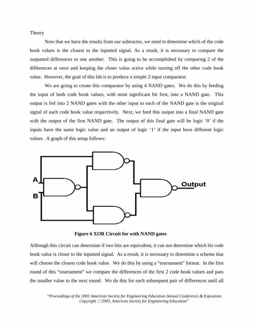
We are going to create this comparator by using 4 NAND gates. We do this by feeding
the input of both code book values, with most significant bit first, into a NAND gate. This
output is fed into 2 NAND gates with the other input to each of the NAND gate is the original
signal of each code book value respectively. Next, we feed this output into a final NAND gate
with the output of the first NAND gate. The output of this final gate will be logic ‘0’ if the
inputs have the same logic value and an output of logic ‘1’ if the input have different logic
values. A graph of this setup follows:
Figure 6 XOR Circuit for with NAND gates
Although this circuit can determine if two bits are equivalent, it can not determine which bit code
book value is closer to the inputted signal. As a result, it is necessary to determine a scheme that
will choose the closest code book value. We do this by using a “tournament” format. In the first
round of this “tournament” we compare the differences of the first 2 code book values and pass
the smaller value to the next round. We do this for each subsequent pair of differences until all
“Proceedings of the 2003 American Society for Engineering Education Annual Conference & Exposition Copyright 2003, American Society for Engineering Education”
of the differences have been compared. This is done for all of the subsequent rounds until the
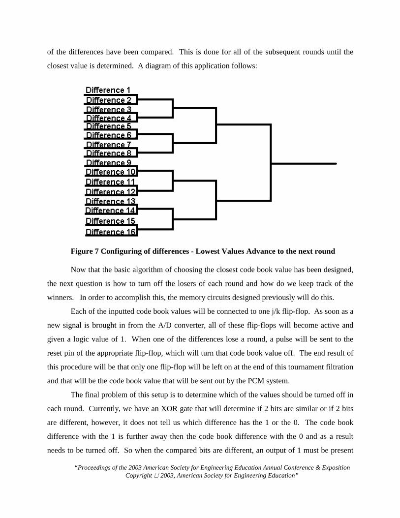
closest value is determined. A diagram of this application follows:
Figure 7 Configuring of differences - Lowest Values Advance to the next round
Now that the basic algorithm of choosing the closest code book value has been designed,
the next question is how to turn off the losers of each round and how do we keep track of the
winners. In order to accomplish this, the memory circuits designed previously will do this.
Each of the inputted code book values will be connected to one j/k flip-flop. As soon as a
new signal is brought in from the A/D converter, all of these flip-flops will become active and
given a logic value of 1. When one of the differences lose a round, a pulse will be sent to the
reset pin of the appropriate flip-flop, which will turn that code book value off. The end result of
this procedure will be that only one flip-flop will be left on at the end of this tournament filtration
and that will be the code book value that will be sent out by the PCM system.
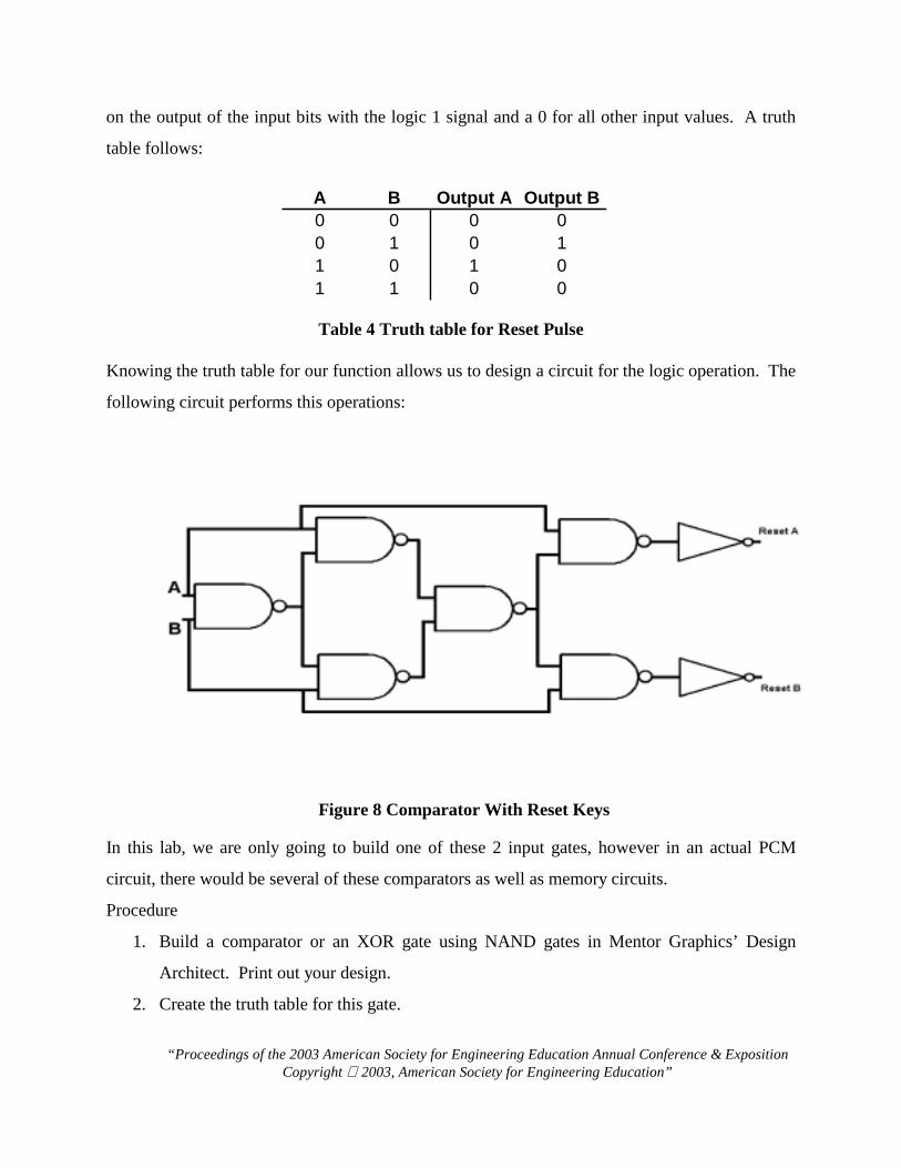
The final problem of this setup is to determine which of the values should be turned off in
each round. Currently, we have an XOR gate that will determine if 2 bits are similar or if 2 bits
are different, however, it does not tell us which difference has the 1 or the 0. The code book
difference with the 1 is further away then the code book difference with the 0 and as a result
needs to be turned off. So when the compared bits are different, an output of 1 must be present
“Proceedings of the 2003 American Society for Engineering Education Annual Conference & Exposition Copyright 2003, American Society for Engineering Education”
on the output of the input bits with the logic 1 signal and a 0 for all other input values. A truth
table follows:
Table 4 Truth table for Reset Pulse
Knowing the truth table for our function allows us to design a circuit for the logic operation. The
following circuit performs this operations:
Figure 8 Comparator With Reset Keys
In this lab, we are only going to build one of these 2 input gates, however in an actual PCM
circuit, there would be several of these comparators as well as memory circuits.
Procedure
1. Build a comparator or an XOR gate using NAND gates in Mentor Graphics’ Design
Architect. Print out your design.
2. Create the truth table for this gate.
A B Output A Output B0 0 0 00 1 0 11 0 1 01 1 0 0
“Proceedings of the 2003 American Society for Engineering Education Annual Conference & Exposition Copyright 2003, American Society for Engineering Education”
3. Simulate this circuit in quicksim and accusim and confirm the validity of your circuit.
Print out all of your simulation results.
*****DO NOT BEGIN LAYOUT AT THIS TIME!!!
4. Reopen Design Architect and add the appropriate NAND gates and inverters to create the
comparator with reset keys. Print out your design.
5. Simulate this circuit in quicksim and accusim and confirm your results with the above
truth table. Print out your simulation results.
6. Open ic station and layout your circuit. Make sure it passes DRC check and LVS. Print
out your LVS report and your layout design.
7. Perform a parasitic extraction of your circuit.
Questions and Conclusions
1. Verify that the given XOR circuit with reset keys gives the appropriate truth table. Hint:
Evaluate the output of every NAND gate and INV for all possible inputs.
2. What are the tradeoffs of block designing vs. MOSFET design?
3. What would happen if the code book differences in a given round were exactly the same?
4. What could you do to rectify this situation?
Experiment 2 – Central Limit Theorem
Objective
To understand and demonstrate the notions of probability, random variable, the
probability density function and the Central Limit Theorem. The materials for this experiment
include a Plinko machine and 100 wooden balls.
Theory
In communication systems today, signals are almost always corrupted with noise after
being sent across a channel. Given a received signal, it is important to determine which one of M
signals was actually transmitted. This is done by calculating the probability of error and choosing
the best candidate of M possible signals as the one that minimizes the probability of error. In this
laboratory, we introduce the concept of probability, random variable, the probability density
function and the Central Limit Theorem [9][16].
“Proceedings of the 2003 American Society for Engineering Education Annual Conference & Exposition Copyright 2003, American Society for Engineering Education”
In order to determine the probability of a certain event happening, engineers set up
random experiments. For an experiment to be random, it must satisfy three requirements: (1) It
must be repeatable under identical conditions, (2) On any trial conducted, the outcome must be
unpredictable and (3) For a large number of trials, the outcomes exhibit statistical regularity,
which means a definite pattern of outcomes emerges. After all of these experiments are run, the
relative frequency of an outcome of a random event is calculated. This is done by calculating the
number of times an event A occurs divided by the number of experiments conducted. The
formula for the relative frequency of an event A is [9]
nnF A
A =
where nA is the number of times event A occurs in n trials. A property closely related to the
relative frequency of a random event is the probability of a random event. The probability of the
random event A is the value of FA as the number of trials, n, approaches infinity. This is denoted
as P(A). or each type of experiment run, there will be m outcomes. For example if we drop a
square box, it will have to land on one of its six sides. Events or outcomes A, B, C, D, E and F
represent the landing on the sides of the box. The set of all possible outcomes is called the
sample space (denoted by S) and P(S) = 1. Instead of saving all of these values as outcomes, a
random variable is used. A random variable, X( ), is a function that takes each outcome of S and
assigns a real number value to that outcome [17]. A sample table displays the events (or
outcomes), probabilities and random variables associated with the dropping of the box. Note that
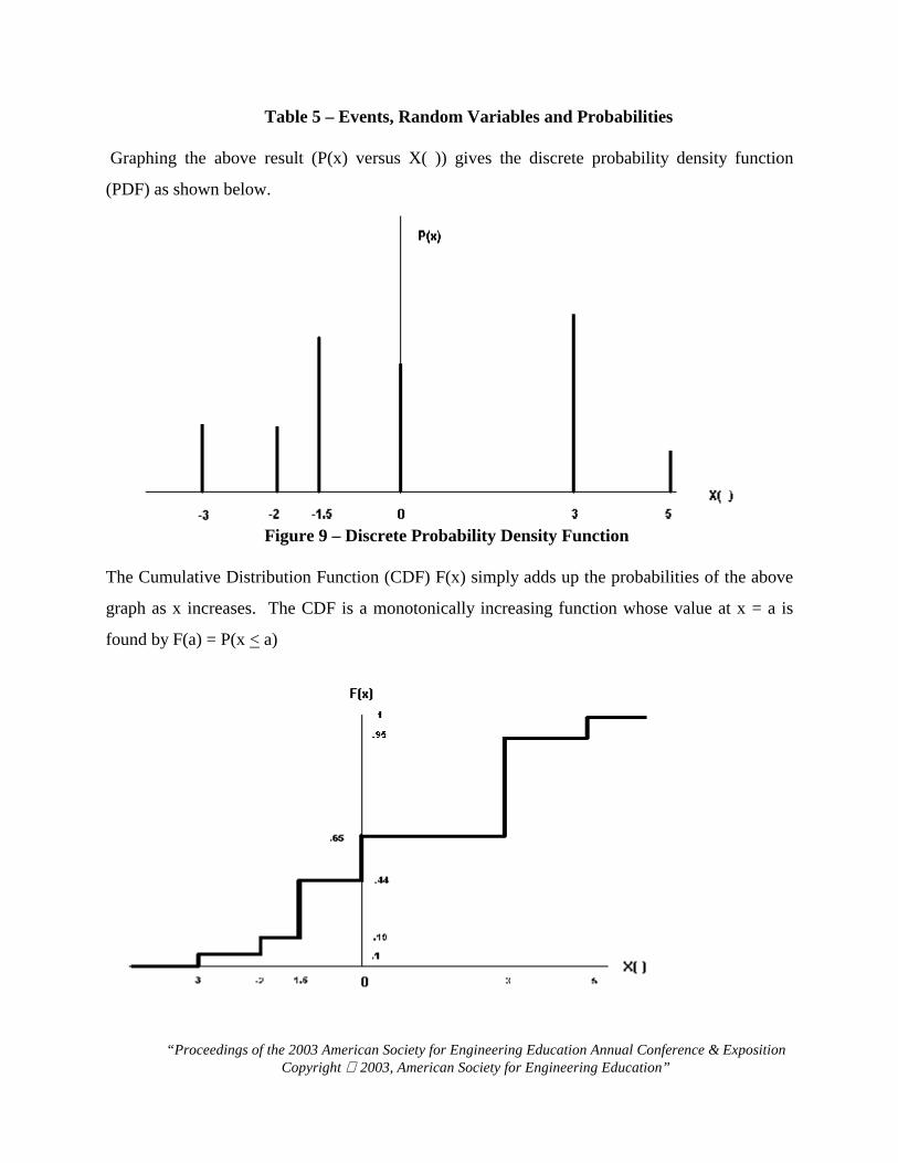
the random variable takes on discrete values.
Event Random Variable X( ) Probability of Event P(x)
A -2.0 0.09 B -1.5 0.25 C -3.0 0.10 D 0.0 0.21 E 3.0 0.30 F 5.0 0.05 Total = 1.00
“Proceedings of the 2003 American Society for Engineering Education Annual Conference & Exposition Copyright 2003, American Society for Engineering Education”
Table 5 – Events, Random Variables and Probabilities
Graphing the above result (P(x) versus X( )) gives the discrete probability density function
(PDF) as shown below.
Figure 9 – Discrete Probability Density Function
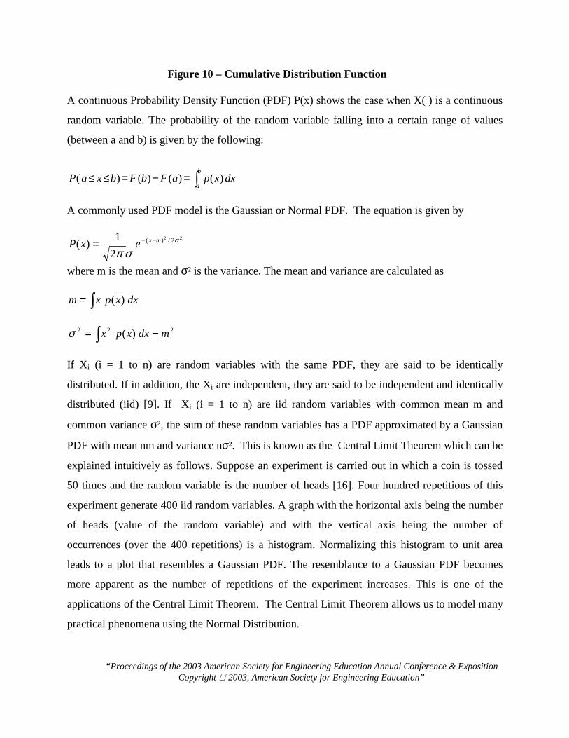
The Cumulative Distribution Function (CDF) F(x) simply adds up the probabilities of the above
graph as x increases. The CDF is a monotonically increasing function whose value at x = a is
found by F(a) = P(x < a)
“Proceedings of the 2003 American Society for Engineering Education Annual Conference & Exposition Copyright 2003, American Society for Engineering Education”
Figure 10 – Cumulative Distribution Function
A continuous Probability Density Function (PDF) P(x) shows the case when X( ) is a continuous
random variable. The probability of the random variable falling into a certain range of values
(between a and b) is given by the following:
∫=−=≤≤b
adxxpaFbFbxaP )()()()(
A commonly used PDF model is the Gaussian or Normal PDF. The equation is given by
22 2/)(
21)( σ
σπmxexP −−=
where m is the mean and σ² is the variance. The mean and variance are calculated as
∫= dxxpxm )(
∫ −= 222 )( mdxxpxσ If Xi (i = 1 to n) are random variables with the same PDF, they are said to be identically
distributed. If in addition, the Xi are independent, they are said to be independent and identically
distributed (iid) [9]. If Xi (i = 1 to n) are iid random variables with common mean m and
common variance σ², the sum of these random variables has a PDF approximated by a Gaussian
PDF with mean nm and variance nσ². This is known as the Central Limit Theorem which can be
explained intuitively as follows. Suppose an experiment is carried out in which a coin is tossed
50 times and the random variable is the number of heads [16]. Four hundred repetitions of this
experiment generate 400 iid random variables. A graph with the horizontal axis being the number
of heads (value of the random variable) and with the vertical axis being the number of
occurrences (over the 400 repetitions) is a histogram. Normalizing this histogram to unit area
leads to a plot that resembles a Gaussian PDF. The resemblance to a Gaussian PDF becomes
more apparent as the number of repetitions of the experiment increases. This is one of the
applications of the Central Limit Theorem. The Central Limit Theorem allows us to model many
practical phenomena using the Normal Distribution.
“Proceedings of the 2003 American Society for Engineering Education Annual Conference & Exposition Copyright 2003, American Society for Engineering Education”
Procedure
1. Place the Plinko Machine in the upright position with the funnel on top.
2. Place 10 wooden balls into the funnel. If the balls get stuck shake the machine gently
until they begin to move again.
3. Observe what compartments the balls come to rest in and drop another 10 balls. Record
the number of balls in each compartment.
4. Continue dropping in 10 balls at a time and record your measurements when you have
dropped 40, 60, 80 and 100 balls.
5. Place cup below bottom hole. Pull out the bottom drawer to empty the machine. Repeat
the experiment again.
Conclusions and Questions
1. How did your outputs compare to the Central Limit Theorem at each step in the
experiment, e.g. at 20, 40, 60, 80, and 100 balls?
2. What could be some reasons why a Normal Distribution would not result in this
experiment?
3. Did all of the 17 containers at the bottom of the Plinko machine contain balls? Which
ones didn’t and why didn’t they have any balls?
4. Were your results from your first trial similar to your second trial? Is this expected and
why?
5. Record any other conclusions you may have reached.
Experiment 3 – Design and Layout of a Hamming Error Correcting Code
Objective
1. To create a circuit specifically designed to encode and decode a 4-bit data word using the
Hamming error correcting code algorithm.
2. To layout the resulting circuit in Mentor Graphics.
Theory
The Hamming error correcting code algorithm [9][14] must be understood before these
objectives can be achieved. The fundamental principle embraced by Hamming codes is parity.
The Hamming weight of a word is defined as the number of binary ‘1’ bits in the data stream.
For example, the code word 11100111 has a Hamming weight of 6 because there are 6 ‘1’ bits
“Proceedings of the 2003 American Society for Engineering Education Annual Conference & Exposition Copyright 2003, American Society for Engineering Education”
present. The Hamming distance between two code words, d, is defined as the number of bits that
differ between the two codewords. For example, given the code words 11001 and 01010, this
has a Hamming distance of 3 because the first, fourth and fifth bits differ from the first code
word to the second.
The purpose of the Hamming codes is to check for errors. It is also possible for a
Hamming decoder to not only detect but also correct these errors if certain conditions are present.
For s errors to be detected and t errors to be corrected, it is required that d > s + t + 1. Also, if
there are no greater than t errors, then these errors can be both detected and corrected if d > 2t +1.
A general code word can be written in the general form:
i1i2i3………ikp1p2p3………pr
in which i are the information bits, p are the parity bits, k are the number of information bits and
r are the number of parity bits. We now define the general form of a Hamming Encoder. In a
(n,k) block code, n = k + r.
The arrangement of parity bits in a code word varies slightly. A block code, which has all
of the information bits at the beginning of the word and all of the parity bits at the end, is called a
systematic block code. A block code that has parity bits interleaved between the information bits
is commonly called an equivalent code.
The smallest Hamming encoder possible is a block code having a Hamming Distance of
3. This occurs because d > 2t + 1. If t =1, then a single error can be detected and corrected. It
also worthwhile to point out that only certain Hamming codes are allowed. These allowable
codes are given by the following formula:
(n,k) = (2m – 1, 2m –1 – m) For a (7,4) Hamming code, the encoder reads in four information bits (I1,I2,I3 and I4) and
outputs three parity bits (P1,P2 and P3) as given by
P3=I4 ⊕ I2 ⊕ I1
P2=I4 ⊕ I3 ⊕ I1
P1=I4 ⊕ I3 ⊕ I2
“Proceedings of the 2003 American Society for Engineering Education Annual Conference & Exposition Copyright 2003, American Society for Engineering Education”
The three parity bits are packaged in with the four information bits and then sent over a
channel after which the bits are presented to the the decoder. We now rewrite these bits keeping
the information bits first. I4, I3, I2, and I1 will be recognized as R7, R6, R5 and R4 respectively
and P3, P2 and P1 will be recognized as R3, R2 and R1, respectively in the decoder example.
The decoder’s job is to receive all seven bits (four information and three parity) and send
out a message that tells you if there is any error or not. If all elements are zero, the codeword was
received correctly. If s contains non-zero elements, the bit in error can be determined by
analyzing which parity checks have failed, as long as the error involves only a single bit for this
specific example of a (7,4) Hamming Encoder. The equations are:
S3=R7 ⊕ R5 ⊕ R4 ⊕ R3
S2=R7 ⊕ R6 ⊕ R4 ⊕ R2
S1=R7 ⊕ R6 ⊕ R5 ⊕ R1
Assignment
Using Mentor Graphics, design the (7,4) Hamming encoder/decoder as two separate circuits. Use
the least amount of board space and fewest FETS possible. Note the dimensions of your circuits.
In your simulation you should show, with hand calculations and your circuit output, that your
Encoder circuit generates the correct code and that the Decoder can detect an error which you
introduce intentionally. The design should be constructed economically. You must perform
parasitic extraction, backannotation and re-simulation with all parasitics.
References
1. K. Jahan, R. A. Dusseau, R. P. Hesketh, A. J. Marchese, R. P. Ramachandran, S. A.
Mandayam and J. L. Schmalzel, ``Engineering Measurements in the Freshman Engineering
Clinic at Rowan University'', ASEE Annual Conference and Exposition, Seattle, Washington,
Session 1326, June 28--July 1, 1998.
2. A. J. Marchese, J. Newell, B. Sukumaran, R. P. Ramachandran, J. L. Schmalzel and J.
Mariappan, ``The Sophomore Engineering Clinic: An Introduction to the Design Process
“Proceedings of the 2003 American Society for Engineering Education Annual Conference & Exposition Copyright 2003, American Society for Engineering Education”
Through a Series of Open Ended Projects'', ASEE Annual Conference and Exposition,
Session 2225, Charlotte, North Carolina, June 20--23, 1999.
3. J. A. Newell, A. J. Marchese, R. P. Ramachandran, B. Sukumaran and R. Harvey,
“Multidisciplinary Design and Communication: A Pedagogical Vision'', International
Journal of Engineering Education, Vol. 15, No. 5, pp. 376-382, 1999.
4. R. M. Felder, “Reaching the Second Tier – Learning and Teaching Styles in College Science
Education”, Journal of College Science Teaching, Vol. 23, No. 5, pp. 285-290, 1993.
5. A. R. Hambley, Electronics, Prentice Hall, 2000.
6. R. Chassaing, Digital Signal Processing Laboratory Experiments Using C and the
TMS320C31 DSK, John Wiley and Sons, 1999.
7. H. V. Sorensen and J. Chen, A Digital Signal Processing Laboratory Experiments Using the
TMS320C30, Prentice Hall, 1997.
8. K. Shenoi, Digital Signal Processing in Telecommunications, Prentice Hall, 1995.
9. Leon W. Couch II, Digital and Analog Communication Systems, Prentice Hall, 1997.
10. N. S. Jayant and P. Noll, Digital Coding of Waveforms: Principles and Applications to
Speech and Video, Prentice-Hall, 1984.
11. S. Orfanidis, Introduction to Signal Processing, Prentice-Hall, New Jersey, 1995.
12. A. V. Oppenheim, R. W. Schafer and J. R. Buck, Discrete-Time Signal Processing, Prentice
Hall, 1999.
13. K. K. Parhi, VLSI Digital Signal Processing Systems: Design and Implementation, John
Wiley and Sons, 1999.
14. I. S. Reed and X. Chen, Error Control Coding for Data Networks, Kluwer, 1999.
“Proceedings of the 2003 American Society for Engineering Education Annual Conference & Exposition Copyright 2003, American Society for Engineering Education”
15. J. F. Wakerly, Digital Design Principles and Practices, Prentice-Hall, 2000.
16. R. D. Yates and D. J. Goodman, Probability and Stochastic Processes, John Wiley and
Sons, 1999.
17. A. Papoulis, Probability, Random Variables and Stochastic Processes, McGraw-Hill, 1991.
Acknowledgement
The authors wish to acknowledge that this work was supported by an NSF CCLI grant (DUE #
0088183).
Biography
Ravi P. Ramachandran is an Associate Professor in the Department of Electrical and Computer
Engineering at Rowan University. He received his Ph.D. from McGill University in 1990 and has
worked at AT&T Bell Laboratories and Rutgers University prior to joining Rowan.
Linda M. Head is an Associate Professor in the Department of Electrical and Computer
Engineering at Rowan University. She received her Ph.D. from the University of South Florida
in 1991 and worked at the State University of New York at Binghamton prior to joining Rowan
University in 1998.
Shreekanth A. Mandayam is an Associate Professor in the Electrical and Computer Engineering
Department at Rowan University. He teaches courses in electromagnetics, communications
systems, digital image processing and artificial neural networks. He conducts research in
nondestructive evaluation and has abiding interests in curriculum innovation and assessment.
John L. Schmalzel has been at Rowan University since 1995, currently serving as Chair of the
Electrical and Computer Engineering Department. He has been active in the development of
Rowan’s new ECE curriculum, with particular interest in the Engineering Clinics, a
multidisciplinary, 8-semester sequence. His other interests include instrumentation and
laboratory development.
“Proceedings of the 2003 American Society for Engineering Education Annual Conference & Exposition Copyright 2003, American Society for Engineering Education”
Steven H. Chin is the Associate Dean of Engineering at Rowan University. He has both research,
laboratory development and teaching experience in Communications, Information Theory,
Digital Signal Processing, Image Processing and Neural Networks. At Rowan, he is the faculty
coordinator for ABET accreditation activities. He joined Rowan after spending 8 years at the


![An Integrated Coimmunications, Digital Signal Processing ...users.rowan.edu/~ravi/conference/conf_2002_04.pdf · include those involving experiments with hardware boards [6][7]. However,](https://static.documents.pub/doc/80x56/60162041b7ee5c15396f91e6/an-integrated-coimmunications-digital-signal-processing-usersrowaneduraviconferenceconf200204pdf.jpg)

