This is an electronic reprint of the original article. This reprint may differ from the original in pagination and typographic detail. Powered by TCPDF (www.tcpdf.org) This material is protected by copyright and other intellectual property rights, and duplication or sale of all or part of any of the repository collections is not permitted, except that material may be duplicated by you for your research use or educational purposes in electronic or print form. You must obtain permission for any other use. Electronic or print copies may not be offered, whether for sale or otherwise to anyone who is not an authorised user. Laitinen, Antti; Paraoanu, G. S.; Oksanen, Mika; Craciun, Monica F.; Russo, Saverio; Sonin, Edouard; Hakonen, Pertti Contact doping, Klein tunneling, and asymmetry of shot noise in suspended graphene Published in: Physical Review B DOI: 10.1103/PhysRevB.93.115413 Published: 09/03/2016 Document Version Publisher's PDF, also known as Version of record Please cite the original version: Laitinen, A., Paraoanu, G. S., Oksanen, M., Craciun, M. F., Russo, S., Sonin, E., & Hakonen, P. (2016). Contact doping, Klein tunneling, and asymmetry of shot noise in suspended graphene. Physical Review B, 93(11), 1-14. [115413]. https://doi.org/10.1103/PhysRevB.93.115413
Transcript
This is an electronic reprint of the original article.This reprint may differ from the original in pagination and typographic detail.
Powered by TCPDF (www.tcpdf.org)
This material is protected by copyright and other intellectual property rights, and duplication or sale of all or part of any of the repository collections is not permitted, except that material may be duplicated by you for your research use or educational purposes in electronic or print form. You must obtain permission for any other use. Electronic or print copies may not be offered, whether for sale or otherwise to anyone who is not an authorised user.
Laitinen, Antti; Paraoanu, G. S.; Oksanen, Mika; Craciun, Monica F.; Russo, Saverio; Sonin,Edouard; Hakonen, PerttiContact doping, Klein tunneling, and asymmetry of shot noise in suspended graphene
Published in:Physical Review B
DOI:10.1103/PhysRevB.93.115413
Published: 09/03/2016
Document VersionPublisher's PDF, also known as Version of record
Please cite the original version:Laitinen, A., Paraoanu, G. S., Oksanen, M., Craciun, M. F., Russo, S., Sonin, E., & Hakonen, P. (2016). Contactdoping, Klein tunneling, and asymmetry of shot noise in suspended graphene. Physical Review B, 93(11), 1-14.[115413]. https://doi.org/10.1103/PhysRevB.93.115413
Contact doping, Klein tunneling, and asymmetry of shot noise in suspended graphene
Antti Laitinen,1 G. S. Paraoanu,1 Mika Oksanen,1 Monica F. Craciun,2 Saverio Russo,2
Edouard Sonin,1,3 and Pertti Hakonen1
1Low Temperature Laboratory, Department of Applied Physics, Aalto University, 00076 AALTO, Finland2Centre for Graphene Science, University of Exeter, EX4 4QL Exeter, United Kingdom3Racah Institute of Physics, Hebrew University of Jerusalem, Jerusalem 91904, Israel
(Received 16 January 2015; revised manuscript received 13 September 2015; published 9 March 2016)
The inherent asymmetry of the electric transport in graphene is attributed to Klein tunneling across barriersdefined by pn interfaces between positively and negatively charged regions. By combining conductance andshot noise experiments, we determine the main characteristics of the tunneling barrier (height and slope) in ahigh-quality suspended sample with Au/Cr/Au contacts. We observe an asymmetric resistance Rodd = 100−70 �
across the Dirac point of the suspended graphene at carrier density |nG| = (0.3−4) × 1011 cm−2, while the Fanofactor displays a nonmonotonic asymmetry in the range Fodd ∼ 0.03–0.1. Our findings agree with analyticalcalculations based on the Dirac equation with a trapezoidal barrier. Comparison between the model and thedata yields the barrier height for tunneling, an estimate of the thickness of the pn interface d < 20 nm, and thecontact region doping corresponding to a Fermi level offset of ∼−18 meV. The strength of pinning of the Fermilevel under the metallic contact is characterized in terms of the contact capacitance Cc = 19 × 10−6 F/cm2.Additionally, we show that the gate voltage corresponding to the Dirac point is given by the difference in workfunctions between the backgate material and graphene.
DOI: 10.1103/PhysRevB.93.115413
I. INTRODUCTION
Klein tunneling is one of the most spectacular effectsof relativistic quantum field theory described by the Diracequation. This tunneling phenomenon, present even in theregime of impenetrable barriers, leads to peculiar transportproperties of graphene. Klein tunneling is the backbone oftransport due to evanescent modes causing the observedpseudodiffusive behavior of ballistic graphene samples [1,2].The bimodal distribution of transmission eigenvalues inballistic graphene coincides with a diffusive conductor, whichresults in shot noise that is indistinguishable from diffusivemesoscopic conductors. Furthermore, the evanescent modeslead to a minimum conductivity of 4e2
πhin the ballistic regime
[3]. Evidence of these Klein tunneling phenomena have beenobtained from observations of charge transport and shot noisein a graphene sheet with ballistic characteristics [4–6].
The most commonly employed assumption in the analysisof the conductance and shot noise of ballistic graphene hasbeen to consider the carbon layer underneath the electrodes asstrongly doped, and this can be modeled using a rectangularelectrostatic potential [1,2,7]. In reality, this assumption suffersfrom severe limitations, as in a real device the charge densityvaries continuously and the rate of change is governed bythe screening length. Various theoretical models for finite-slope potentials have been analyzed for pn interfaces ingraphene [8–10]. All the models have predicted asymmetryin transport properties with respect to the gate voltage, i.e.,whether the charge carriers are electrons or holes. Suchasymmetry has been observed in recent experiments [11–14].In the ballistic regime this asymmetry is attributed to Kleintunneling [14–16], while scattering by charged impurities[17,18] also plays a role in the diffusive regime. Furthermore,evidence of Klein tunneling has been reported in conductance
interfaces have also been achieved in nonsuspended samplesusing air-bridge-type gates [21,22]. A full understanding ofcontact issues is of vital importance for the developmentof novel electrical components using graphene and othertwo-dimensional materials [23]. In particular, a detailedunderstanding of pn interfaces is critical for optoelectronicscomponents [24].
The asymptotic carrier transport in Klein tunneling is boundto be affected by the strong influence of the metal contactson graphene. A simple contact model was formulated byGiovannetti et al. [25], who also performed density functionaltheory (DFT) calculations concerning the involved workfunctions. In this paper, we generalize this model to include theeffects of the applied backgate voltage, and we combine theresulting model with tunneling calculations based on the Diracequation in order to obtain a comprehensive transport modelfor analyzing electrical conduction in a ballistic suspendedgraphene sample. We employ a trapezoidal form for thetunneling barrier, which we show how to treat analytically [26].By using conductance and shot noise experiments performedon a high-quality suspended graphene sample, we can deter-mine the barrier parameters and their relation to the dopingof the graphene by a metallic contact. In comparison withDFT calculations [25], we find semiquantitative agreementfor the graphene-modified metal work functions as wellas for the distance between the charge separation layersthat govern the contact capacitance between the metal andgraphene.
The experiment and the agreement with the theoreticalmodel confirm the existence of Klein tunneling in graphene.Our method works well even in the situation in which thework functions of the contact metal and graphene differ
ANTTI LAITINEN et al. PHYSICAL REVIEW B 93, 115413 (2016)
by a relatively small amount (tens of meV). As such, ourresults suggests an alternative method to find the workfunction of materials. Note that the difference in workfunctions between two metals is not measurable directly:the standard way for its determination is the use of Kelvinprobe force microscopy, where the electrical capacitancebetween the metal and a probe is varied in order to inducea measurable ac current. Our results demonstrate that thereexists a gating effect in the position of the Dirac point ofthe suspended graphene due to the work function of thebackgate. Thus, by using a material as the backgate forgraphene and measuring the gate voltage corresponding to theDirac point, one can get a simple dc measurement of the workfunction.
The paper is organized as follows: We present a completetheoretical treatment of the problem of gated suspendedgraphene with metallic contacts in Sec. II. The structure ofour samples is detailed in Sec. III together with the employedmethods for shot noise measurements. Our experimentalresults and their analysis are presented in Sec. IV. Theimplications of the results are discussed in Sec. V jointly witha comparison to other works.
II. THEORETICAL BACKGROUND
A. Electrochemical model for suspended graphene samples
When a graphene sheet is brought into contact with ametal, electrons will flow between them in order to equilibratethe Fermi level. This effect has been analyzed in detail inRefs. [25,27]. We proceed beyond these works and introducea complete electrochemical model for a suspended graphenesample with metallic contact electrodes. Our model takes intoaccount consistently the effect of the backgate on the dopingof the graphene under the metal. We show that this effectcan be neglected only if the difference between the workfunction of the metallic contact electrode and the graphenelayer is large enough [i.e., in the limit of a high barrier, definedbelow Eq. (17)]. If this is not the case, the contact-regiondoping acquired from the backgate voltage has to be includedin the transport calculations. In addition to the electrostaticcontributions, our model indicates that the difference inwork functions between the backgate and graphene entersthe equilibrium charge density, which, in particular, leadsto a small shift in the Dirac point of the suspended part ofthe graphene. Using electrochemical equilibrium conditions,we derive analytical equations that incorporate all theseeffects.
In Fig. 1(a), we present a schematic sideview of the sample,showing the region of contact with the metal and the grapheneas well as the backgate. For clarity, we have exaggerated thesize of some components, so the figure is not to scale. Onthe sample chip, the graphene sheet is placed at a distance ofdG = 300 nm from the backgate. The sheet is supported bya SiO2 insulating layer (εr = 3.9), which is partially etchedaway under the graphene. This results in a vacuum gap ofheight dvac = 150 nm. Further details on the sample and themetallic contacts can be found in Sec. III.
Mgncn
Ggnvacd
Gd
r
M g
gG
Mn
Gn
cd
z
x
FME
ceUGWMn
gMeU
MgC
gV
gMn
cn
geV
cWG
cC
c
gW
MW
MW
GW
gW
z M- sectiong
FGE
Gn
gGeU
geV
GW
Ggn
gGCGW gW
gW
G- sectiongz
(a)
(b)
(c)
FIG. 1. Schematic of the sample and of the electrochemicalpotentials. (a) Section perpendicular to the graphene sheet (pink),showing the metal M (gray) on top, a contact layer (yellow) ofwidth dc, the support dielectric (beige), and the backgate (gray)g, at a distance dG under the graphene layer. As seen in the crosssection, we assume that the underetching of SiO2 below the graphenecan be regarded as small. (b) Schematic of the electrochemicalpotentials for the graphene under the metal (along the line M-g).(c) Schematic of the electrochemical potential for the suspendedgraphene (along the line G-g). For a definition of the other symbols,see the text.
115413-2
CONTACT DOPING, KLEIN TUNNELING, AND . . . PHYSICAL REVIEW B 93, 115413 (2016)
In our sample structure, the capacitance per unit area CgM
between the graphene and the backgate in the support region(graphene under the metal) is estimated from the regularparallel plate formula
CgM = ε0εr
dG, (1)
which yields CgM ∼ 1.2 × 10⁻⁸ F/cm2 using the above-mentioned values for dG and εr . In the suspended region,the graphene capacitance per unit area against the backgateCgG can be calculated using the formula for two capacitors inseries: a vacuum capacitor with a plate separation of dvac anda capacitor with the spacing dG − dvac filled with dielectricmaterial having εr . This results in the capacitance per unit area
CgG = ε0
dG + (dG − dvac)(ε−1r − 1
) . (2)
In our calculations, the actual value for the suspended partcapacitance is taken from our Fabry-Perot measurementsCgG = 4.7 × 10⁻⁹ F/cm2 [16], which agrees well with theabove theoretical value.
Next, we analyze the electrochemical potentials that appearin this experimental setting. We take two cuts through Fig. 1(a),one across the dashed line M-g, and the other across thedashed line G-g, and we represent the spatial variation of theelectrochemical potential in Figs. 1(b) and 1(c), respectively.The work function of the pristine graphene is denoted by WG.At the contact with the metal, this work function may bemodified by a small shift; see Ref. [25]. The work functionof the contact metal on top of the graphene is denoted byWM, while the work function of the backgate is Wg . Notethat according to Volta’s rule, the contact potential at the endof a circuit is determined only by the work functions of thecircuit elements at the end; therefore, no other work function,for example corresponding to various other metals along themeasurement chain, can enter in this problem. The differencebetween the work function of the gate and that of grapheneis denoted by eVDirac = Wg − WG: this quantity will turn outto be the shift of the Dirac point of the suspended regionof graphene due to the backgate work function. Followingcommon practice in graphene research, gate voltages in thefollowing formulas will be measured with respect to the Diracpoint, with the corresponding shifts defined as
δVg = Vg − VDirac. (3)
We first solve the problem of finding the surface chargedistribution for the electrochemical potentials presented inFig. 1(b). At the contact between the metal and the graphene,the electrons will move from the electrode with the lower workfunction into the electrode with the higher work function.As a result, a surface charge distribution enc will appearin the contact region, producing an electrostatic potential
Uc = enc/Cc across the contact capacitance Cc, the magnitudeof which reflects the spatial variation of the surface charge.According to DFT calculations, Cc � 10−5 F/cm2 [25]. Arelevant parameter for charge transfer between the metal andgraphene is the difference between the work functions of thegraphene under the metal and the work function of the metal,which is described by
χ = WG + �c − WM, (4)
where WM is the work function of the metallic contact materialand WG + �c denotes the modified work function of thegraphene under the contact. Another electrostatic potentialUgM = engM/CgM is established across the capacitance CgM,with a surface charge engM on the gate. The total particle-number surface density nM in the graphene layer in the contactregion is therefore
nM = ngM + nc. (5)
The first equilibrium condition is obtained from the condi-tion that the difference between the Fermi level of the metal andthat of the gate equals eVg . This condition does not formallyinvolve the characteristic density of states of graphene. Hence,as shown by the circuit schematics below the Fermi leveldiagram in Fig. 1(b), it can be regarded as a pure electrostaticcondition. It states
eδVg = χ + eUgM − eUc. (6)
The second equation governing the equilibrium involvesthe intrinsic properties of graphene, and it can be obtained byusing the condition that the Fermi levels of the metal and thegraphene under the metal coincide:
�EFM + eUc = χ. (7)
In the graphene under the metal, where the linear graphenebands are supposed to persist, the relation between the numberof negatively charged carriers per unit area nM and the shift inthe Fermi level �EFM is given by
�EFM = �vFsgn(nM)√
π |nM|, (8)
where vF = 1.1 × 10⁶ m/s is the Fermi velocity. It is usefulto introduce a constant ζF relating the Fermi speed and thefundamental constants � and e:
ζF =√
π�vF
e. (9)
We propose to call this quantity “Fermi electric flux.” Thisconstant is related to the concept of quantum capacitance (forgraphene, see Ref. [28]) and to the fine-structure constant ofgraphene, as detailed in Appendix A. The Fermi electric fluxdetermines the energy shifts produced by graphene as it isinserted into an electrical circuit. For vF = 1.1 × 10⁶ m/s, theequation yields ζF = 1.283 × 10⁻⁷ V cm.
Combining now Eqs. (5)–(8), and choosing the properphysical solution, we obtain the final result for the shift ofthe energy level of graphene under the metal,
�EFM = sgn
[δVg + χCc
eCgM
]⎧⎨⎩−Cc + CgM
2ζ 2
F +√(
Cc + CgM
2ζ 2
F
)2
+ ζ 2F Cc
∣∣∣∣χ + CgM
Cc
eδVg
∣∣∣∣⎫⎬⎭. (10)
115413-3
ANTTI LAITINEN et al. PHYSICAL REVIEW B 93, 115413 (2016)
An experimentally relevant limit for Eq. (10) is the case of avery large contact capacitance Cc: if the material parametersare such that (Cc + CgM)ζ 2
F � |χ | and the charge inducedby the gate voltage is relatively small, then eCgM|δVg| �Cc|χ |, and we obtain �EFM ≈ χ from Eq. (10). In thissituation, the large contact capacitance locks the position ofthe Dirac point of the graphene under the metal to a value�EFM set by the parameter χ . Also note that by using thecorrespondence concerning charge density ncl due to classicaldoping and gating, e2|ncl| → Cc|χ + CgM
CceδVg|, sgn(ncl) →
sgn(δVg + χCc
eCgM), one can show that Eq. (10) coincides
with the results of Ref. [29] in the case of twogates.
In our experimental setup, in fact, χ remains relativelysmall, which makes the quantity eCgMδVg/Cc comparablewith χ at large values of δVg . Consequently, the Fermilevel can even reach the Dirac point of the graphene underthe metal, �EFM = 0. As the latter condition does requiresubstantial gate voltages, we could not reach this regime inour experiment.
Next we turn to the suspended part of the graphene. In thisregion, the charge accumulated on the surface of the backgate,ngG, which produces a voltage drop UgG = engG/CgG, isexactly compensated by the charges on the graphene sidehaving the particle-number surface density nG,
nG = ngG. (11)
Then, the condition that the electrochemical potential differ-ence between the Fermi level of graphene and the Fermi levelof the backgate is eVg reads
eδVg = eUgG + �EFG, (12)
where
�EFG = �vFsgn(nG)√
π |nG|, (13)
in parallel to Eq. (8). From Eqs. (11)–(13), we find for theFermi level shift in the suspended part (see also Refs. [29,30]),
�EFG = sgn(δVg)
{−CgG
2ζ 2
F
+√(
CgG
2ζ 2
F
)2
+ eCgGζ 2F |δVg|
}. (14)
Note that �EFG = 0 corresponds to δVg = 0, i.e., Vg =VDirac is indeed the Dirac point of the suspended graphene.For �EFG, typical experimental conditions fulfill e|δVg| �|χ | � CgGζ 2
F , which allows one to approximate �EFG ≈sgn(δVg)ζF
√eCgG|δVg|. This limit was assumed in the pre-
vious analysis by Sonin [26].The difference of the Fermi energies of the suspended
graphene and the graphene under the contact results in anelectrostatic potential difference V0 between the free-standingregion of graphene and the one under the metal:
eV0 = �EFM − �EFG. (15)
This leads to a potential barrier for the electrons travelingalong the x direction, from one metallic contact to the other,as detailed in the next subsection. Since transmission through
the potential barrier is first and foremost sensitive to the slopeof the barrier at the charge-neutrality point, we have adopteda trapezoidal barrier shape where the slope is constant onboth sides of the flat top of the barrier. This trapezoidalform is tractable using analytical calculations, and it isexpected to catch the basic features of the tunneling transportproblem.
B. Klein tunneling: Conductance and Fano factor
The asymmetry in electrical transport across a basic,backgated graphene device is related to many aspects of thesample, its quality, and biasing conditions. It depends on thenature of transport, i.e., whether it is ballistic or diffusive, onthe presence of interfaces between p- and n-doped regions,on the steepness of the slopes of the electrostatic potentialbarrier, on the doping due to the contacts, and on the coherenceof the transport between the reflecting interfaces (pn-typeinterface or two unipolar regions with different doping, eitherp and p′ or n and n′, yielding pp′ and nn′ interfaces). Thetype of junction is determined by the sign of the Fermi levelshifts: if �EFM > 0 and �EFG > 0, we have an nn′ junctionat the left contact; if �EFM < 0 and �EFG > 0, we havea pn junction; if �EFM > 0 and �EFG < 0, we have annp junction; and if �EFM < 0 and �EFG < 0, we have app′ junction. The same notions apply to the right contactprovided that the regions are considered from right to left,instead of the left-to-right direction used for the left contactabove.
Our experimental data deal with suspended graphene with amean free path on the order of the sample length. Consequently,we will consider first and foremost Klein tunneling in theballistic regime and neglect the influence of disorder [31].Unlike the early work discussed above, we take into accountthe weak doping of contact regions when using Au/Cr/Auleads. We assume symmetric contacts, although in reality thereis always slight asymmetry. In our context, this assumptionmeans that the values of the work function difference χ areequal at both contacts. The asymmetry of the contact resistancecan be neglected as the contact resistance is found to beinsignificant in the analysis. The use of moderate voltagesand cryogenic temperatures also guarantees a negligible roleof acoustic phonons [32].
Below, we derive the formulas for the transmission andreflection coefficients, as well as the conductance and Fanofactor, for the tunneling geometry given in Fig. 2. The figureshows variation of the electrostatic potential (see Fig. 1) inthe x direction along the whole graphene sheet, includingthe end contacts. We consider only propagating modes; thisapproximation is justified by the criterion that propagationthrough the evanescent modes can be neglected if the biasvoltages are clearly above �vF /eL [7], where L is the lengthof the sample. For a typical sample of length L = 1 μm,�vF /eL = 0.7 mV, well below the bias voltages used in ourexperiments for shot noise (10–70 mV).
The use of the Dirac equation with a trapezoidal barrieris the simplest approximation for transport in a two-leadgraphene sample with a pair of pn interfaces due to spatiallyvarying charge doping. The electrostatic trapezoidal barrier (ofstructure nn′n) in Fig. 2 is comprised of five distinct regions:
115413-4
CONTACT DOPING, KLEIN TUNNELING, AND . . . PHYSICAL REVIEW B 93, 115413 (2016)
M G M
e
FIG. 2. Schematic view of a trapezoidal nn′n barrier configura-tion across the sample. V0 denotes the difference in the electrostaticpotential between the contact regions and the center. The solid redline shows variation of the electrostatic potential along the graphenesheet (see also Fig. 1); the kinks of the red line separate the fivedifferent spatial regions in which the Dirac equation is solved. Theslope of V (x) in the range −d � x � 0 is a�vF/e.
the middle part 0 � x � L, corresponding to the region G fromthe previous subsection, where there is a step in electrostaticpotential V0 (the difference in the potential between the contactregions and the center); two sloped regions −d � x � 0and L � x � L + d in the vicinity of the graphene/metalinterfaces, where the electric field is finite; and finally thecontact area x � −d and L + d � x with zero (or small bias)potential, corresponding to the region M of graphene fullycovered by the contact metal. Dirac electrons propagatingalong the x direction may thus experience Klein tunnelingunder this barrier. In the left slope region −d � x � 0, thepotential is written in the form V (x) = V0 + sgn[V0]a �vF
ex.
The parameter a sets the absolute value of the voltage slope.In general, the barrier can have either a positive or a negativeslope, depending on the sign of V0. For clarity, we will give theexplicit analytical forms of the solutions of the Dirac equationonly for the case of positive slope, corresponding to the leftside of the barrier in Fig. 2. The solutions for negative slopecan be obtained by the same procedure.
All the energies are measured from the Dirac point of thegraphene under the metal, with the standard convention that�EFM is positive if the Fermi level is above the Dirac point andnegative otherwise; see Eqs. (8) and (10). A similar conventionis used for �EFG; see Eqs. (13) and (14).
The massless Dirac equation for a graphene sheet can bewritten as[
−i∂
∂xσz − i
∂
∂yσy
]�(x,y) = K(x)�(x,y), (16)
where for particles near the Fermi level K(x) = [�EFM −eV (x)]/�vF, and the upper and lower components of the spinor�(x,y) are denoted by ψ+(x,y) and ψ−(x,y), respectively. σz
is a Pauli matrix coming from the rotation of the original DiracHamiltonian in Ref. [26]. Note that the electrons at the Fermilevel will have energy �EFM in any of the regions M, G, or inthe slope region. We can solve the Dirac equation in Eq. (16)by the method of separation of variables, writing ψ±(x,y) =ψ±(x) exp(ikyy), with the current along the x direction jx =evF(|ψ+|2 − |ψ−|2) normalized to ±evF.
The height of the energy barrier eV0 = �EFM − �EFG
defines a step eV0/�vF in the momentum of the Dirac
electrons as they cross the barrier. The influence of thischange in momentum can be characterized compactly using adimensionless parameter, the impact parameter, defined as
p0 = eV0
�vF√
a. (17)
The impact parameter will play an essential role in ourcalculations below. Note that the earlier theoretical treatmentby Sonin [26] assumed a large impact parameter |p0| � 1.As this approximation is not valid for our present exper-iment, a finite p0 needs to be taken into account in thetheory.
Assuming that the thickness of the sloped region d isindependent of the gate voltage, we can express the absolutevalue of the slope of the barrier in terms of the Vg-dependentquantities, �EFM and �EFG, which yields
a =√
π
ζFd|V0|. (18)
Likewise, we obtain for the impact parameter
p0 = sgn(V0)
(√πd
ζF
)1/2√|V0|. (19)
Note that the impact parameter increases with the absolutevalue of the slope, as evident from Eqs. (17) and (18).
1. Top of the barrier, x > 0 (region G)
In this region, we consider an electron moving to the right,jx = evF. The Dirac equation can be solved, with
K(x|x > 0) = 1
�vF�EFG, (20)
for both positive and negative �EFG,(ψ+(x)ψ−(x)
)∣∣∣∣x>0
=(
12 + kx,FG±iky
2kFG
− 12 + kx,FG±iky
2kFG
)√kFG
kx,FGe±ikx,FGx, (21)
where the ± sign denotes sgn(�EFG). The absolute value ofthe wave vector is
kFG = |�EFG|�vF
, (22)
and kx,FG =√
k2FG − k2
y . Note that ky remains unchanged overall region crossings.
2. Slope of the barrier, −d < x < 0
In this region, we have
K(x| − d < x < 0) = −sgn(V0)a(x − x0), (23)
depending on whether the slope is positive or negative. Here x0
is the crossing point, defined as the position where the kernelis nullified, and it is given by x0 = sgn(V0)�EFG/a�vF. In thisregion, one can use Sauter’s solution for the Dirac electron in ahomogeneous electric field (see Ref. [26]). For positive slope,with the substitution ξ (x) = √
a(x − x0), we have
ψ+(x)|−d<x<0 = C1F (ξ (x),ky/√
a) + C2G∗(ξ (x),ky/
√a),
ψ−(x)|−d<x<0 = C1G(ξ (x),ky/√
a) + C2F∗(ξ (x),ky/
√a).
115413-5
ANTTI LAITINEN et al. PHYSICAL REVIEW B 93, 115413 (2016)
Note also that the dimension of a is (length)−2, while that ofK(x) and ky is (length)−1, hence the quantity ky/
√a, which
enters the hypergeometric functions, is adimensional.The functions F and G are defined through the Kummer
confluent hypergeometric function M ≡1 F1,
F (ξ,κ) = e−iξ 2/2M
(− iκ2
4,1
2,iξ 2
)(24)
and
G(ξ,κ) = −κξe−iξ 2/2M
(1 − iκ2
4,3
2,iξ 2
). (25)
From the boundary conditions at x = 0 we obtain
C1 = kFG + kx,FG + i sgn(�EFG)ky
2√
kFGkx,FGF ∗(ξ (0),ky/
√a)
+ kFG − kx,FG − i sgn(�EFG)ky
2√
kFGkx,FGG∗(ξ (0),ky/
√a),
(26)
C2 = −kFG + kx,FG + i sgn(�EFG)ky
2√
kFGkx,FGF (ξ (0),ky/
√a)
− kFG + kx,FG + i sgn(�EFG)ky
2√
kFGkx,FGG(ξ (0),ky/
√a).
(27)
Importantly, a consequence of the normalization |ψ+|2 −|ψ−|2 = 1 is the fact that |C1|2 − |C2|2 = 1 and |F (ξ,κ)|2 −|G(ξ,κ)|2 = 1, which can be verified explicitly using theexplicit expressions above.
3. Graphene under the metal x < −d (region M)
In the calculation of Sonin [26], this region with x < −d
was disregarded on the basis of the assumption p20 � 1. It
turns out that this condition is not valid in our experiment (cf.Fig. 5), and the behavior in the region x < −d has to be takeninto account. In this region,
K(x|x < −d) = 1
�vF�EFM. (28)
The absolute value of the total momentum at the Fermi levelis then
kFM = 1
�vF|�EFM|. (29)
The corresponding momentum in the x direction is equalto kx,FM =
√k2
FM − k2y , and the wave is a superposition of
a reflected and a transmitted component,
(ψ+(x)ψ−(x)
)∣∣∣∣x<−d
= 1
t
(12 + kx,FM±iky
2kFM
− 12 + kx,FM±iky
2kFM
)√kFM
kx,FMe±ikx,FMx
+ r
t
(12 + −kx,FM±iky
2kFM
− 12 + −kx,FM±iky
2kFM
)√kFM
kx,FMe∓ikx,FMx.
(30)
Here r and t are the reflection and transmission amplitudes,± is the sign of sgn(�EFM), and ∓ in the last exponent is−sgn(�EFM).
Note also that in Eq. (30) the reflected component is normal-ized to the current in the x direction, equal to −evF, while thetransmitted component is normalized to +evF. However, onecan explicitly check that the overall normalization of �(x,y)is to +evF, provided that |r|2 + |t |2 = 1. This ensures that thenormalization is the same for all three regions. To understandintuitively how this is realized, note that the admixture of thereflection component in �(x,y) of Eq. (30) is compensated byan increase in the component propagating to the right, since|t | becomes subunitary.
By imposing the condition of continuity of the wavefunction at x = −d, after some algebra we obtain the complextransmission amplitude,
1
te−ikx,FMd
= −−kFM − kx,FM + i sgn(�EFM)ky
2√
kFMkx,FM
× [C1F (ξ (−d),ky/√
a) + C2G∗(ξ (−d),ky/
√a)]
+ kFM − kx,FM + i sgn(�EFM)ky
2√
kFMkx,FM
× [C1G(ξ (−d),ky/√
a) + C2F∗(ξ (−d),ky/
√a)].
(31)
C. Conductance and Fano factor for the whole barrier
To calculate the total transmission through the barrier, weemploy the incoherent addition of the transmission coeffi-cients. Usually phase coherence is more sensitive to disorderthan reflection and transmission, and we address the case inwhich the former is destroyed but the latter is not affected bydisorder (the ballistic regime). This assumption is supported bythe experimental fact that the Fabry-Perot resonances are foundto be weak. Furthermore, when destroying the Fabry-Perotresonances fully by an applied bias, the overall conductancedoes not change much. Hence, we consider the incoherenttreatment of transmission probabilities well justified in ouranalysis.
In general, for the case of incoherent tunneling through asymmetric barrier with equal transmission T for the left andright slopes, the total probability of transmission through thebarrier is (see Appendix B)
Ttot = 1
2T −1 − 1. (32)
By using the Landauer-Buttiker formalism, we obtain theconductance and the Fano factor as sums over the transmissioncoefficients and their quadratic values. Each quantized valueof ky corresponds to a conduction channel, over which thesummation of transmission coefficients has to be performedin order to obtain the total conductance (shot noise) from theconductance per channel (shot noise per channel). Thus, for asample with a given level of contact doping �EFM, one cancalculate the conductance σ and the Fano factor F as a function
115413-6
CONTACT DOPING, KLEIN TUNNELING, AND . . . PHYSICAL REVIEW B 93, 115413 (2016)
of gate voltage. In the limit of a large number of channels, σ
and F can be written as
σ = 4e2W
πh
∫ min{kFM,kFG}
0dkyTtot, (33)
F = 1 − 1
σ
∫ min{kFM,kFG}
0dkyT
2tot. (34)
The conductance and the Fano factor will depend on Vg
through the dependence of the quantities kFG, kFM, �EFG, and�EFM obtained previously. If the contact resistance betweenthe graphene and the metal is neglected, then the input toEq. (32) is given by T = |t |2, where |t |2 = |t(ky)|2 is thetransmission coefficient calculated using Eq. (31).
If a finite contact resistance exists, then a finite transmissionprobability 0 � Tc � 1 should be included in the value of T
in Eq. (32). By the reasoning outlined in Appendix B, we maywrite
T = Tc|t |2Tc + |t |2 − Tc|t |2 . (35)
The inclusion of contact resistance has a strong influence onthe shot noise, and the calculated Fano factor becomes quicklylarger than the measured value when the contact transmissionis lowered from 1.
The limits of integration in Eqs. (33) and (34) are set bythe condition that the wave vector kx is a real number, in otherwords the electron is not in a bound state but propagates toinfinity. The condition ky < kFG comes from the top of thebarrier region, while the condition ky < kFM comes from theregion x < −d.
Interestingly, even with our potential profile with fivedistinct regions as shown in Fig. 2, the entire model has onlytwo essential fitting parameters, namely p0 = eV0/�vF
√a =
sgn(V0)√
ad and the barrier slope a. The impact parametercontains information on the doping via Eqs. (8), (14), and(15), and it enters in the upper limit of the integrals in Eqs. (33)and (34), since kFM = |√ap0 + �EFG/�vF|. In fact, the Fanofactor in our calculation is fully determined by the value ofp0, while the conductance integrals need also the value of thebarrier slope for their evaluation.
III. SAMPLE AND SHOT NOISE METHODS
The measured suspended sample was manufactured usingstandard PMMA-based e-beam lithographic techniques on agraphene piece exfoliated onto Si/SiO2 chip (see Fig. 3). Thedashed white line with two circles in the figure indicatesthe positions at which one obtains the cross-sectional viewdepicted in Fig. 1(a); the circles correspond to the spots atwhich the electrochemical potential profiles (along the verticaldirection) are drawn in Figs. 1(b) and 1(c). The graphenesample was contacted with Au/Cr/Au leads of thickness5/7/50 nm, after which roughly 135 nm of the sacrificialsilicon dioxide was etched away using hydrofluoric acid (HF)following the methods discussed in Refs. [33,34]. Ramanspectroscopy was employed to verify the single-layer structureof the graphene sample. Current annealing at Vg = 0 was usedto enhance the mobility of the sample. We employed voltagebias around 1 V and a current of (0.3−0.7) μA/μm in our
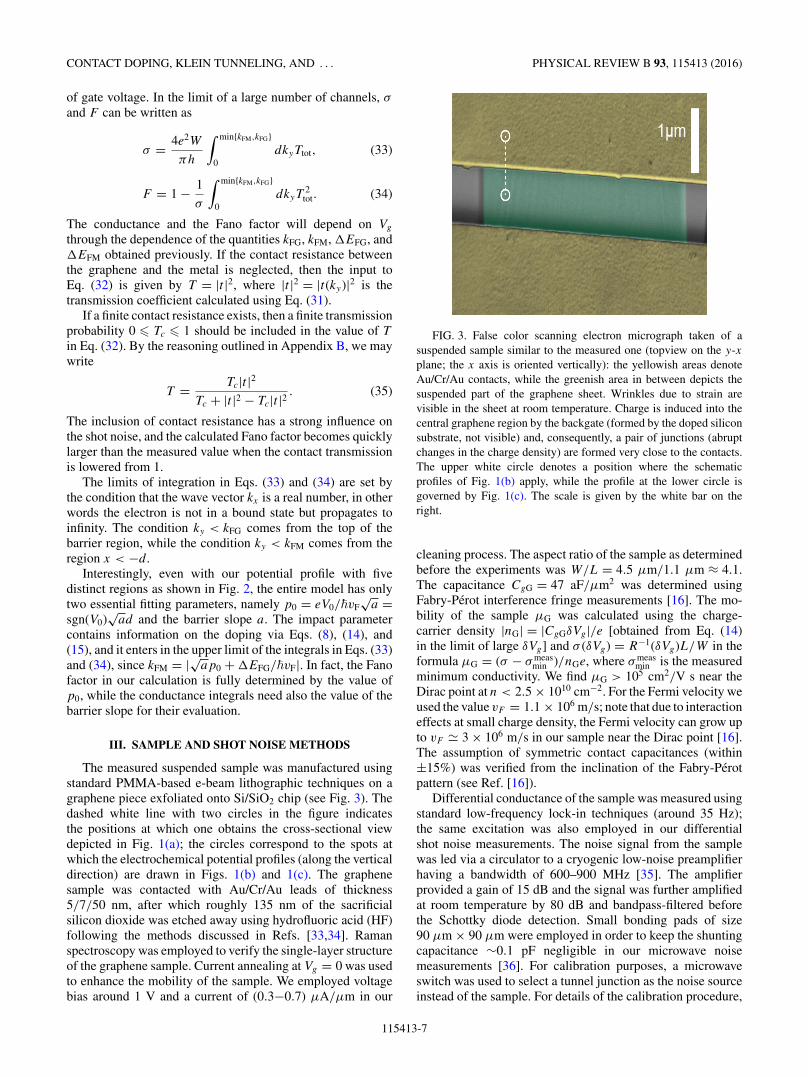
FIG. 3. False color scanning electron micrograph taken of asuspended sample similar to the measured one (topview on the y-xplane; the x axis is oriented vertically): the yellowish areas denoteAu/Cr/Au contacts, while the greenish area in between depicts thesuspended part of the graphene sheet. Wrinkles due to strain arevisible in the sheet at room temperature. Charge is induced into thecentral graphene region by the backgate (formed by the doped siliconsubstrate, not visible) and, consequently, a pair of junctions (abruptchanges in the charge density) are formed very close to the contacts.The upper white circle denotes a position where the schematicprofiles of Fig. 1(b) apply, while the profile at the lower circle isgoverned by Fig. 1(c). The scale is given by the white bar on theright.
cleaning process. The aspect ratio of the sample as determinedbefore the experiments was W/L = 4.5 μm/1.1 μm ≈ 4.1.The capacitance CgG = 47 aF/μm2 was determined usingFabry-Perot interference fringe measurements [16]. The mo-bility of the sample μG was calculated using the charge-carrier density |nG| = |CgGδVg|/e [obtained from Eq. (14)in the limit of large δVg] and σ (δVg) = R−1(δVg)L/W in theformula μG = (σ − σ meas
min )/nGe, where σ measmin is the measured
minimum conductivity. We find μG > 105 cm2/V s near theDirac point at n < 2.5 × 1010 cm−2. For the Fermi velocity weused the value vF = 1.1 × 10⁶ m/s; note that due to interactioneffects at small charge density, the Fermi velocity can grow upto vF � 3 × 10⁶ m/s in our sample near the Dirac point [16].The assumption of symmetric contact capacitances (within±15%) was verified from the inclination of the Fabry-Perotpattern (see Ref. [16]).
Differential conductance of the sample was measured usingstandard low-frequency lock-in techniques (around 35 Hz);the same excitation was also employed in our differentialshot noise measurements. The noise signal from the samplewas led via a circulator to a cryogenic low-noise preamplifierhaving a bandwidth of 600–900 MHz [35]. The amplifierprovided a gain of 15 dB and the signal was further amplifiedat room temperature by 80 dB and bandpass-filtered beforethe Schottky diode detection. Small bonding pads of size90 μm × 90 μm were employed in order to keep the shuntingcapacitance ∼0.1 pF negligible in our microwave noisemeasurements [36]. For calibration purposes, a microwaveswitch was used to select a tunnel junction as the noise sourceinstead of the sample. For details of the calibration procedure,
115413-7
ANTTI LAITINEN et al. PHYSICAL REVIEW B 93, 115413 (2016)
Vg (V)-15 -10 -5 0 5 10 15
R-1
(S)
×10-3
0
1
2
3
4
5
6
theoryexperiment
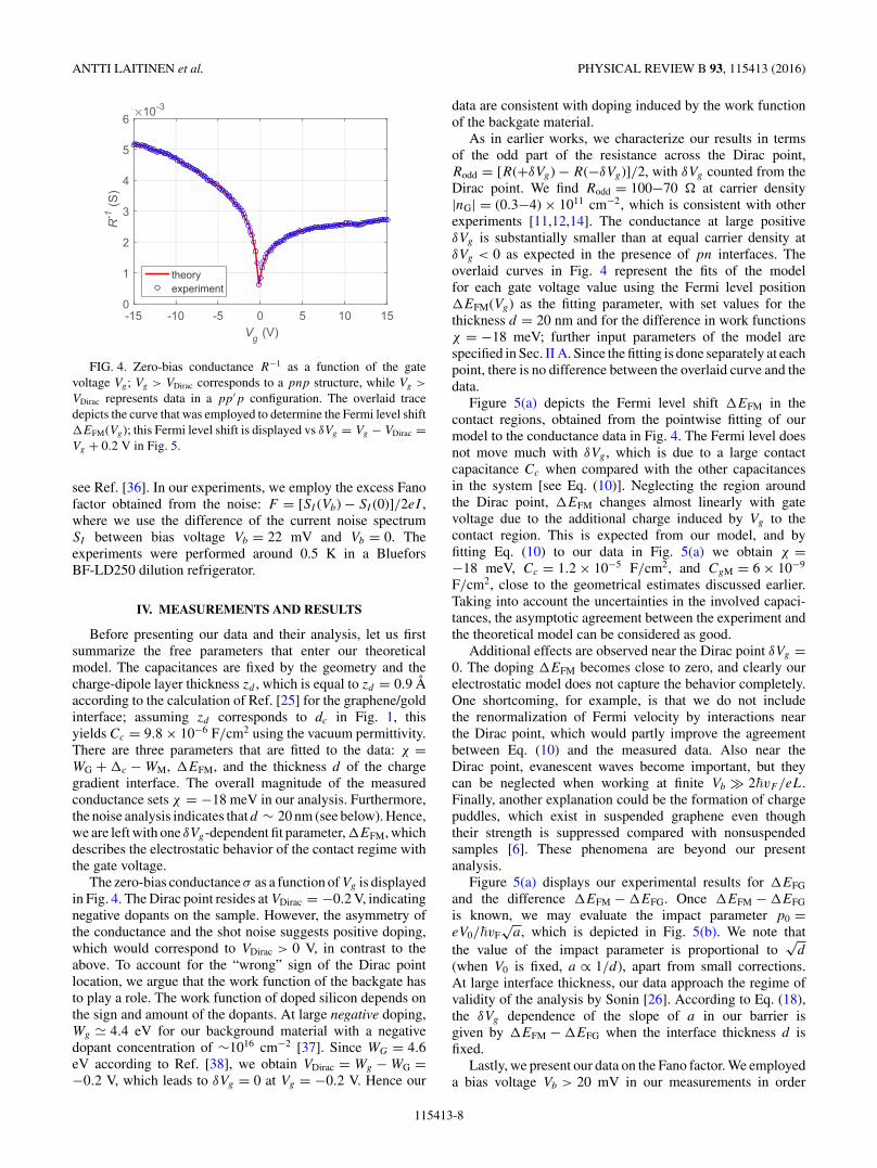
FIG. 4. Zero-bias conductance R−1 as a function of the gatevoltage Vg; Vg > VDirac corresponds to a pnp structure, while Vg >
VDirac represents data in a pp′p configuration. The overlaid tracedepicts the curve that was employed to determine the Fermi level shift�EFM(Vg); this Fermi level shift is displayed vs δVg = Vg − VDirac =Vg + 0.2 V in Fig. 5.
see Ref. [36]. In our experiments, we employ the excess Fanofactor obtained from the noise: F = [SI (Vb) − SI (0)]/2eI ,where we use the difference of the current noise spectrumSI between bias voltage Vb = 22 mV and Vb = 0. Theexperiments were performed around 0.5 K in a BlueforsBF-LD250 dilution refrigerator.
IV. MEASUREMENTS AND RESULTS
Before presenting our data and their analysis, let us firstsummarize the free parameters that enter our theoreticalmodel. The capacitances are fixed by the geometry and thecharge-dipole layer thickness zd , which is equal to zd = 0.9 Aaccording to the calculation of Ref. [25] for the graphene/goldinterface; assuming zd corresponds to dc in Fig. 1, thisyields Cc = 9.8 × 10⁻⁶ F/cm2 using the vacuum permittivity.There are three parameters that are fitted to the data: χ =WG + �c − WM, �EFM, and the thickness d of the chargegradient interface. The overall magnitude of the measuredconductance sets χ = −18 meV in our analysis. Furthermore,the noise analysis indicates that d ∼ 20 nm (see below). Hence,we are left with one δVg-dependent fit parameter, �EFM, whichdescribes the electrostatic behavior of the contact regime withthe gate voltage.
The zero-bias conductance σ as a function of Vg is displayedin Fig. 4. The Dirac point resides at VDirac = −0.2 V, indicatingnegative dopants on the sample. However, the asymmetry ofthe conductance and the shot noise suggests positive doping,which would correspond to VDirac > 0 V, in contrast to theabove. To account for the “wrong” sign of the Dirac pointlocation, we argue that the work function of the backgate hasto play a role. The work function of doped silicon depends onthe sign and amount of the dopants. At large negative doping,Wg � 4.4 eV for our background material with a negativedopant concentration of ∼1016 cm−2 [37]. Since WG = 4.6eV according to Ref. [38], we obtain VDirac = Wg − WG =−0.2 V, which leads to δVg = 0 at Vg = −0.2 V. Hence our
data are consistent with doping induced by the work functionof the backgate material.
As in earlier works, we characterize our results in termsof the odd part of the resistance across the Dirac point,Rodd = [R(+δVg) − R(−δVg)]/2, with δVg counted from theDirac point. We find Rodd = 100−70 � at carrier density|nG| = (0.3−4) × 1011 cm−2, which is consistent with otherexperiments [11,12,14]. The conductance at large positiveδVg is substantially smaller than at equal carrier density atδVg < 0 as expected in the presence of pn interfaces. Theoverlaid curves in Fig. 4 represent the fits of the modelfor each gate voltage value using the Fermi level position�EFM(Vg) as the fitting parameter, with set values for thethickness d = 20 nm and for the difference in work functionsχ = −18 meV; further input parameters of the model arespecified in Sec. II A. Since the fitting is done separately at eachpoint, there is no difference between the overlaid curve and thedata.
Figure 5(a) depicts the Fermi level shift �EFM in thecontact regions, obtained from the pointwise fitting of ourmodel to the conductance data in Fig. 4. The Fermi level doesnot move much with δVg , which is due to a large contactcapacitance Cc when compared with the other capacitancesin the system [see Eq. (10)]. Neglecting the region aroundthe Dirac point, �EFM changes almost linearly with gatevoltage due to the additional charge induced by Vg to thecontact region. This is expected from our model, and byfitting Eq. (10) to our data in Fig. 5(a) we obtain χ =−18 meV, Cc = 1.2 × 10⁻⁵ F/cm2, and CgM = 6 × 10⁻⁹
F/cm2, close to the geometrical estimates discussed earlier.Taking into account the uncertainties in the involved capaci-tances, the asymptotic agreement between the experiment andthe theoretical model can be considered as good.
Additional effects are observed near the Dirac point δVg =0. The doping �EFM becomes close to zero, and clearly ourelectrostatic model does not capture the behavior completely.One shortcoming, for example, is that we do not includethe renormalization of Fermi velocity by interactions nearthe Dirac point, which would partly improve the agreementbetween Eq. (10) and the measured data. Also near theDirac point, evanescent waves become important, but theycan be neglected when working at finite Vb � 2�vF /eL.Finally, another explanation could be the formation of chargepuddles, which exist in suspended graphene even thoughtheir strength is suppressed compared with nonsuspendedsamples [6]. These phenomena are beyond our presentanalysis.
Figure 5(a) displays our experimental results for �EFG
and the difference �EFM − �EFG. Once �EFM − �EFG
is known, we may evaluate the impact parameter p0 =eV0/�vF
√a, which is depicted in Fig. 5(b). We note that
the value of the impact parameter is proportional to√
d
(when V0 is fixed, a ∝ 1/d), apart from small corrections.At large interface thickness, our data approach the regime ofvalidity of the analysis by Sonin [26]. According to Eq. (18),the δVg dependence of the slope of a in our barrier isgiven by �EFM − �EFG when the interface thickness d isfixed.
Lastly, we present our data on the Fano factor. We employeda bias voltage Vb > 20 mV in our measurements in order
115413-8
CONTACT DOPING, KLEIN TUNNELING, AND . . . PHYSICAL REVIEW B 93, 115413 (2016)
δVg (V)-15 -10 -5 0 5 10 15
E (
meV
)
-100
-50
0
50
100
E (exp)FG
EFM - EFG
EFM (exp)
EFM (Eq. (10))
(a)
δVg (V)-15 -10 -5 0 5 10 15
p0
-4
-2
0
2
4d = 1 nmd = 20 nmd = 100 nm
(b)
FIG. 5. (a) Position of the Fermi level �EFM in the contact regionobtained from the experimental data for the conductance presentedin Fig. 4 (orange symbols), the Fermi level position in the suspendedpart �EFG (blue symbols), and the difference �EFM − �EFG (redsymbols). The solid line is the dependence obtained from Eq. (10)using χ = −18 meV; the values of the contact capacitances arediscussed in the text. (b) Variation of the impact parameter p0 withgate voltage obtained from the �EFM − �EFG data presented above;p0 < 0 corresponds to the pnp configuration. The behavior dependson the thickness d , the values of which are indicated in the figure.
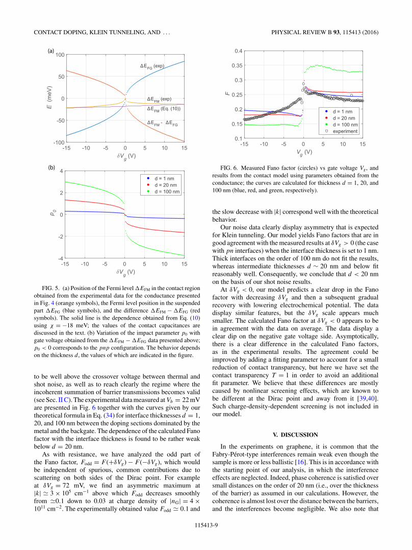
to be well above the crossover voltage between thermal andshot noise, as well as to reach clearly the regime where theincoherent summation of barrier transmissions becomes valid(see Sec. II C). The experimental data measured at Vb = 22 mVare presented in Fig. 6 together with the curves given by ourtheoretical formula in Eq. (34) for interface thicknesses d = 1,20, and 100 nm between the doping sections dominated by themetal and the backgate. The dependence of the calculated Fanofactor with the interface thickness is found to be rather weakbelow d = 20 nm.
As with resistance, we have analyzed the odd part ofthe Fano factor, Fodd = F (+δVg) − F (−δVg), which wouldbe independent of spurious, common contributions due toscattering on both sides of the Dirac point. For exampleat δVg = 72 mV, we find an asymmetric maximum at|k| � 3 × 105 cm−1 above which Fodd decreases smoothlyfrom �0.1 down to 0.03 at charge density of |nG| = 4 ×1011 cm−2. The experimentally obtained value Fodd � 0.1 and
Vg (V)-15 -10 -5 0 5 10 15
F
0.1
0.15
0.2
0.25
0.3
0.35
0.4
d = 1 nmd = 20 nmd = 100 nmexperiment
FIG. 6. Measured Fano factor (circles) vs gate voltage Vg , andresults from the contact model using parameters obtained from theconductance; the curves are calculated for thickness d = 1, 20, and100 nm (blue, red, and green, respectively).
the slow decrease with |k| correspond well with the theoreticalbehavior.
Our noise data clearly display asymmetry that is expectedfor Klein tunneling. Our model yields Fano factors that are ingood agreement with the measured results at δVg > 0 (the casewith pn interfaces) when the interface thickness is set to 1 nm.Thick interfaces on the order of 100 nm do not fit the results,whereas intermediate thicknesses d ∼ 20 nm and below fitreasonably well. Consequently, we conclude that d < 20 nmon the basis of our shot noise results.
At δVg < 0, our model predicts a clear drop in the Fanofactor with decreasing δVg and then a subsequent gradualrecovery with lowering electrochemical potential. The datadisplay similar features, but the δVg scale appears muchsmaller. The calculated Fano factor at δVg < 0 appears to bein agreement with the data on average. The data display aclear dip on the negative gate voltage side. Asymptotically,there is a clear difference in the calculated Fano factors,as in the experimental results. The agreement could beimproved by adding a fitting parameter to account for a smallreduction of contact transparency, but here we have set thecontact transparency T = 1 in order to avoid an additionalfit parameter. We believe that these differences are mostlycaused by nonlinear screening effects, which are known tobe different at the Dirac point and away from it [39,40].Such charge-density-dependent screening is not included inour model.
V. DISCUSSION
In the experiments on graphene, it is common that theFabry-Perot-type interferences remain weak even though thesample is more or less ballistic [16]. This is in accordance withthe starting point of our analysis, in which the interferenceeffects are neglected. Indeed, phase coherence is satisfied oversmall distances on the order of 20 nm (i.e., over the thicknessof the barrier) as assumed in our calculations. However, thecoherence is almost lost over the distance between the barriers,and the interferences become negligible. We also note that
115413-9
ANTTI LAITINEN et al. PHYSICAL REVIEW B 93, 115413 (2016)
strong Fabry-Perot interferences have been observed withdifferent contact materials [15], which might be a result ofhigher contact doping (|EFG| � |EFM|) and a different chargeprofile in those samples. In addition, our noise experimentswere performed at finite bias, above the regime where Fabry-Perot oscillations were observed, which may strengthen thetendency toward incoherent behavior; in fact, electron-electroninteraction effects in disordered graphene have been foundto be 100 times larger in graphene than in regular metallicsystems [41].
The difference in work functions including the chemicalinteraction �c was found to be related to the overall magnitudeof the sample conductance, which set χ = WG − WM + �c =−18 meV. In our notation, χ < 0 corresponds to positivedoping if �EFM is solely governed by χ .
For gold contacts (WM = 4.7 eV), DFT calculations predictχ � −0.1, . . . , − 0.2 eV [25,42], but one has to keep in mindthat these calculations yield the work function of pure goldwith an error on the order of 0.2 eV. Experiments suggestthat χ = −0.35 eV for pure gold [43]. Furthermore, Crhas a work function of WM = 4.5 eV, and Cr/Au contactshave been shown to yield a work function of 4.3 eV forgraphene under the contact [44], which leads to an estimateχ � −0.2 eV for Cr/Au contacts. The results of Ref. [45]suggest χ = −0.1 eV for the Au/Cr contact, although theauthors discuss that the contact doping might be close to zero,which would be in agreement with our results. However, theexact comparison with Ref. [45] is problematic because of thedifferences in the contact structure: we evaporate first 5 nm ofAu before laying down 7 nm of Cr. As discussed below, thevacancy creation by the first evaporated metal layer is of majorconcern.
The actual electrical contacting is further complicated bythe reactivity of metal atoms on top of graphene [46,47].Using in situ x-ray photoelectron spectroscopy, it has beendemonstrated that sometimes the side-contacting picture maybe misleading with real contacts [48]. In our analysis, forsimplicity, we need to assume a uniform graphene layer underthe metallic contact, although it is possible that metals likeCr promote vacancy formation and lead to the creation ofdefects under the evaporated metal; similar defect formationhas been reported due to deposition of gold atoms [49], as wellas in annealing studies of metallic contacts [50]. Furthermore,charge transfer at the interface depends on the amount ofoxygen and nitrogen on top of graphene, as has been found infunctionalization studies by Foley et al. [51].
Despite possible defect formation, gold contacts are knownto preserve the graphene cone structure under the contact[52,53]. Quantum capacitance measurements of grapheneunder the contact were performed in Ref. [53] to characterizethe cone structures. The accuracy of these quantum capacitancedeterminations compared with theory is within a factor of 2.These findings suggest a modification of the Fermi velocityunder the contacts. An inclusion of such a modification wouldform a promising extension of our theory, but this was left forfuture work.
The parameter �EFM together with gate capacitance(yielding �EFG) determines fully the product da, whichvaries strongly with the gate voltage. Hence, our measurementimposes a constraint on the product da as a function of δVg .
When the thickness of the interface is fixed, the slope ofthe interface quickly approaches zero as �EFM − �EFG →0. Altogether, the range of variation of �EFM − �EFG israther limited, which indicates weak doping by contactingmetal as well as by the gate (CgG is small for suspendeddevices).
The same analysis as presented here can be performedusing a constant slope a rather than a fixed d. We didsuch an analysis, and, somewhat surprisingly, the numericalsimulations yielded similar predictions for the conductivityand Fano factor, in particular for Rodd and Fodd. This increasesthe confidence in the analysis of our results, demonstrating thatthe extraction of relevant parameters does not depend stronglyon model-specific assumptions about the trapezoidal barrierin the regime of our data (i.e., at small interface thickness d).Additionally, recent independent experiments [34] reportingdirect observation of the band gap in ABC-stacked trilayergraphene have shown that the chosen trapezoidal shapefor V (x) with fixed-width edges also governs the residualtunnel conductance in few-layer graphene, extending thevalidity of our model to a broad range of systems wellbeyond the single-layer pn-junction case presented in thispaper.
Screening influences the speed at which charge densityvaries across borders between differently doped regions. Dueto its peculiar inherent properties, screening in graphene maybe strongly nonlinear. According to theory [40], the screeninginfluences mostly the asymptotic behavior of the barrier,whether it is x−1/2 or x−1, but not much the length scaleof the rapid initial relaxation. Since we use a trapezoidalshape and neglect the relaxation behavior in the barrieraltogether, we have chosen to work with a fixed thickness,which is proportional to the average inverse slope of the chargerelaxation at the pn interface. One should keep in mind thatour analysis is not reliable close to the Dirac point since therethe slope itself weakly affects the conductance. Therefore, ourfitting is mostly sensitive to the interfacial thickness far awayfrom the Dirac point, where the screening length becomesshort.
According to Ref. [40], the approximate thickness of thepn interface could be in the range of 5 nm (see also Ref. [54]),which is consistent with our results d < 20 nm. Full numericalsimulations on the pn-interface structure in a double-gatedgraphene structure have been performed in Ref. [55]. Withinthe trapezoidal approximation, the calculated slope of thepotential profile in Ref. [55] yields an interface thicknessof 30–40 nm. In our case, the leads may act as gates and,consequently, the pn interfaces near the contacts remainsharp, in agreement with theoretical estimates. Our interfacialwidth of d ∼ 20 nm, on the other hand, is much smallerthan that found using scanning photocurrent microscopy onnonsuspended samples fabricated on silicon dioxide [56,57].
Our primary fit parameter �EFM takes into account thestandard electrostatics in the contact region. Our analysisindicates a clear success of electrostatic analysis, and theresults verify the large role of contact capacitance arising dueto charge transfer between the contact metal and graphene.This leads to pinning of the Fermi level at the contact, whichis consistent with the findings in Refs. [56,57]. Near the Diracpoint, we find modifications from the standard electrostatic
115413-10
CONTACT DOPING, KLEIN TUNNELING, AND . . . PHYSICAL REVIEW B 93, 115413 (2016)
doping picture, which are presumably related to the neglect ofproper screening treatment and nonuniformities in the chargedistribution near the Dirac point.
Finally, our analysis is based on a rather idealized theoreti-cal model. Additional effects can be included in our theoreticalmodel, for example the broadening of the density of states inthe graphene due to inhomogeneities and due to coupling tometal. Clearly, the inclusion of these effects would broaden theconductance and the Fano factor characteristics, resulting in abetter fit with our experimental data. The disadvantage of thisphenomenological approach is that supplementary knowledgeon additional parameters would be needed. We did check,however, what happens if a finite contact resistance is includedusing Eq. (35). From the simulations, we find that a significantdiscrepancy in the overall value of the Fano factor starts toappear for Tc < 0.9: the Fano factor increases quickly overthe entire gate voltage range, and the fitting becomes difficultregardless of how large the doping is. This constrains the valueof Tc to ∼0.95–1, but the improvements in the fitting achievedwithin this range are negligibly small.
In conclusion, we have developed a practical transportmodel for analyzing transport in ballistic suspended graphenesamples. Our analysis shows how the doping in graphenedepends on the difference between the work function ofthe metal and graphene as well as on the applied gatevoltage measured from the Dirac point, which is given bythe work-function difference between the backgate materialand graphene. By combining conductance and shot noiseexperiments performed on a high-quality suspended graphenesample, we have determined all the relevant parameters thatare involved in the electrostatics of the contact and in theKlein tunneling of graphene. When comparing with DFTcalculations [25], we find semiquantitative agreement for thegraphene-modified metal work functions as well as for thedistance between the charge separation layers, which governthe contact capacitance between the metal and graphene. Thesmall charge layer separation (∼1 A) leads to a large contactcapacitance, which is responsible for the rather weak tunabilityof the Fermi level position under the contact.
ACKNOWLEDGMENTS
We acknowledge fruitful discussions with D. Cox, V. Falko,T. Heikkila, M. Katsnelson, M.-H. Liu, and A. De Sanctis. Ourwork was supported by the Academy of Finland (ContractNo. 250280, LTQ CoE) and by the Graphene Flagship project.This research project made use of the Aalto UniversityCryohall infrastructure. S.R. and M.F.C acknowledge finan-cial support from EPSRC (Grants No. EP/J000396/1, No.EP/K017160/1, No. EP/K010050/1, No. EPG036101/1, No.EP/M001024/1, and No. EPM002438/1) and from Royal So-ciety international Exchanges Scheme2012/R3 and 2013/R2.
APPENDIX A: THE FERMI ELECTRIC FLUX
The Fermi electric flux
ζF =√
π�vF
e(A1)
is related to the concept of quantum capacitance per unit areaof graphene,
Cq = e2D(�EF) = e2 dn
d(�EF), (A2)
where n is the number of excess (negatively charged) carriersper unit area, D(�EF) is the density of states of graphene, and�EF is the energy of the Fermi level measured from the Diracpoint,
�EF = �vFsgn(n)√
π |n| = eζFsgn(n)√
|n|. (A3)
Another useful formula is |n| = (�EF/eζF)2. With thesenotations, one immediately obtains
�EF = 12Cqζ
2F , (A4)
resembling the formula for the energy 12CV 2 of a capacitor C
charged by a fixed voltage V . Therefore, the Fermi electric fluxis the electric flux through the plates of a capacitor of unit areaand unit distance between the plates, with capacitance equalto the quantum capacitance and charged to an electrostaticenergy �EF.
The Fermi electric flux is a useful constant also forstudying the inductive properties of graphene. The dualitybetween the electric and magnetic properties is manifested inthis case through the simple relation ζF = vF�0/
√π , where
�0 = h/2e is the flux quantum. Then, the graphene kineticinductance can be defined by regarding the Fermi energy εF
as a magnetic energy associated with the magnetic flux ζF/vF,yielding
LG,kin = ζ 2F
v2FεF
, (A5)
in agreement with the known result for the kinetic inductanceof graphene [58].
Another connection can be made with the fine-structureconstant, α = e2/4πε0�c ≈ 1/137, which has an essential rolein determining the optical properties of graphene [59]. Weobtain
ζF = evF
4√
πε0αc. (A6)
Similarly, one can introduce a graphene fine-structureconstant αG = e2/4πε0�vF = αc/vF ≈ 2, obtaining ζF =e/4
√πε0αG.
APPENDIX B: CONDUCTANCEFOR THE WHOLE BARRIER
Equation (32) is well known in mesoscopic physics and canbe found in some textbooks, e.g., by Datta [60] and by Nazarovand Blanter [61]. It is derived by summing over all the Fabry-Perot reflection and transmission processes and neglecting theinterference term in the final result [60]. Here we give analternative, simpler proof, starting from the beginning withthe assumption that the currents simply add up without anyinterference term.
We consider the generic problem of incoherent tunnelingthrough two interfaces: interface 1 separating the left regionfrom a middle region and interface 2 separating the middle
115413-11
ANTTI LAITINEN et al. PHYSICAL REVIEW B 93, 115413 (2016)
)( lj
)( lj
)( rj)(bj
)(bj
left barrier right
FIG. 7. Generic schematic for tunneling through two interfaces,separating a middle region (b) from the left (l) and the right (r)regions.
region from the right region; see Fig. 7. Typically in this typeof problem, the middle region is associated with a barrier, so wewill denote it as such. The barrier has transmission coefficientsT1 on the left side and T2 on the right side; the correspond-ing reflection coefficients are denoted by R1 = 1 − T1 andR2 = 1 − T2.
We assume that a wave producing a current j (l)→ propagates
from the left (l) region toward the barrier. Part of this wavewill get reflected back to the left into j (l)
← , and part of it getstransmitted in the region under the barrier (b), with the currentj (b)→ . At the right side of the barrier, the incoming current j (b)
→gets transmitted to the region on the right of the barrier (r) asj (r)→ , and part of it is reflected back under the barrier as j (b)
← . Thewave j (b)
← travels backward (to the left) toward the left side ofthe barrier, where it is partly reflected and partly transmitted,contributing to j (b)
→ and j (l)← , respectively. By using the fact that
in the absence of interference the currents will just sum up, weget
j (r)→ = T2j
(b)→ , (B1)
j (b)← = R2j
(b)→ , (B2)
j (b)→ = T1j
(l)→ + R1j
(b)← , (B3)
j (l)← = R1j
(l)→ + T1j
(b)← . (B4)
Adding the first pair of equations (B1) and (B2) yields theconservation law for the current at the (b)-(r) interface, j (r)
→ =j (b)→ − j (b)
← , while adding the second pair, Eqs. (B3) and (B4),gives the conservation law at the (l)-(b) interface, j (l)
→ − j (l)← =
j (b)→ − j (b)
← . From these two equations, we get j (l)→ − j (l)
← = j (r)→ ,
which is a conservation law across the entire barrier. Finally,by combining Eqs. (B1) and (B3) we get
j (r)→ = T1T2
1 − R1R2j (l)→, (B5)
from which we can read directly the overall transmissioncoefficient across the barrier, Ttot = T1T2/(1 − R1R2). ForT1 = T2 = T , this yields
Ttot = 1
2T −1 − 1, (B6)
which was given in Eq. (32) of the main text. Similarly, fromEqs. (B2)–(B4) we obtain
j (l)← = R1 + R2 − 2R1R2
1 − R1R2j (l)→, (B7)
from which we get the overall reflection coefficient across thebarrier, Rtot = (R1 + R2 − 2R1R2)/(1 − R1R2).
APPENDIX C: FINITE BIAS
The model presented in the paper does not include the smallvoltage bias used in the experiment to create a nonzero electriccurrent between the left and the right contacts. A small finitebias voltage Vb can be easily included, as detailed below. Weassume that this bias is equally distributed, Vb/2 between theleft metal and the graphene and −Vb/2 between the right metaland the graphene sheet. We also assume that the currents aresmall enough so that the equilibrium structure of the energylevels in graphene is not considerably changed. The bias onlyprovides a slightly higher Fermi level in the metal from whichelectrons are injected at the left side and holes are injected at theright side. Due to electron-hole symmetry, the total current andthe total noise can be calculated by adding the contributionscorresponding to electron and hole transport [7].
The electron injected from the left into the graphene sheetwill have a Fermi energy shift in the metal contact region�EFM + eVb/2, and a Fermi energy shift �EFG + eVb/2in the suspended region. Similarly, for the hole injectedfrom the right side, we will have the shifts �EFM −eVb/2 and �EFG − eVb/2. The current at a bias voltageVb + dVb can be calculated in this model by taking intoaccount that this voltage will be distributed onto bothjunctions, dj = σ (+)dVb/2 + σ (−)dVb/2. The measured con-ductance for a bias voltage Vb is defined as σ = dj/dVb,yielding
σ = 12 [σ (+) + σ (−)]. (C1)
Similarly, the differential noise for a bias voltage Vb is
s = 12 [s(+) + s(−)], (C2)
and the Fano factor becomes
F = s
σ. (C3)
In these equations, σ (±) and s(±) are the same as σ and s
introduced in Sec. II, but they are now calculated for electronswith energies �EFM ± eVb/2, �EFG ± eVb/2 shifted fromthe equilibrium values calculated in Eqs. (10) and (14), andcorrespondingly shifted momenta [see Eqs. (22) and(29)],k
(±)FG = |�EFM ± eVb/2|�vF and k
(±)FM = |kFM ± eVb/2|�vF. To
summarize,
σ (±) = 4e2W
πh
∫ min{k(±)FM ,k
(±)FG }
0dkyT
(±)tot , (C4)
s(±) = 4e2W
πh
∫ min{k(±)FM ,k
(±)FG }
0dky[1 − T
(±)tot ]T (±)
tot , (C5)
where T(±)
tot is defined according to Eq. (32), but at energies�EFM ± eVb/2, �EFG ± eVb/2, and at shifted momenta k
(±)FM,
k(±)FG .
Note that due to the assumptions above, the impactparameter p0 and the slope a will not change, since these arecalculated from the equilibrium values eV0 = �EFM − �EFG
115413-12
CONTACT DOPING, KLEIN TUNNELING, AND . . . PHYSICAL REVIEW B 93, 115413 (2016)
and a = √π |V0|/ζFd. Using this modified model, we can
account for the effect of a small bias voltage. The simulationshows that, as expected, this produces a slight broadening of
the ideal (zero-bias) conductance and Fano factor, and it doesnot have a significant effect for the determination of the dopingparameters.
[1] J. Tworzydlo, B. Trauzettel, M. Titov, A. Rycerz, and C.Beenakker, Phys. Rev. Lett. 96, 246802 (2006).
[2] M. I. Katsnelson, K. S. Novoselov, and A. K. Geim, Nat. Phys.2, 620 (2006).
[3] M. I. Katsnelson, Eur. Phys. J. B 51, 157 (2006).[4] F. Miao, S. Wijeratne, Y. Zhang, U. C. Coskun, W. Bao, and
C. N. Lau, Science 317, 1530 (2007).[5] R. Danneau, F. Wu, M. Craciun, S. Russo, M. Tomi, J.
Salmilehto, A. Morpurgo, and P. Hakonen, Phys. Rev. Lett. 100,196802 (2008).
[6] X. Du, I. Skachko, A. Barker, and E. Y. Andrei, Nat.Nanotechnol. 3, 491 (2008).
[7] E. B. Sonin, Phys. Rev. B 77, 233408 (2008).[8] V. V. Cheianov and V. I. Fal’ko, Phys. Rev. B 74, 041403(R)
(2006).[9] A. Shytov, M. Rudner, and L. Levitov, Phys. Rev. Lett. 101,
156804 (2008).[10] J. Cayssol, B. Huard, and D. Goldhaber-Gordon, Phys. Rev. B
79, 075428 (2009).[11] B. Huard, J. Sulpizio, N. Stander, K. Todd, B. Yang, and D.
Goldhaber-Gordon, Phys. Rev. Lett. 98, 236803 (2007).[12] B. Huard, N. Stander, J. Sulpizio, and D. Goldhaber-Gordon,
Phys. Rev. B 78, 121402 (2008).[13] A. L. Grushina, D.-K. Ki, and A. F. Morpurgo, Appl. Phys. Lett.
102, 223102 (2013).[14] N. Stander, B. Huard, and D. Goldhaber-Gordon, Phys. Rev.
Lett. 102, 026807 (2009).[15] P. Rickhaus, R. Maurand, M.-H. Liu, M. Weiss, K. Richter, and
C. Schonenberger, Nat. Commun. 4, 2342 (2013).[16] M. Oksanen, A. Uppstu, A. Laitinen, D. J. Cox, M. F. Craciun,
S. Russo, A. Harju, and P. Hakonen, Phys. Rev. B 89, 121414(2014).
[17] D. S. Novikov, Appl. Phys. Lett. 91, 102102 (2007).[18] J.-H. Chen, C. Jang, S. Adam, M. S. Fuhrer, E. D. Williams, and
M. Ishigami, Nat. Phys. 4, 377 (2008).[19] A. F. Young and P. Kim, Nat. Phys. 5, 222 (2009).[20] A. F. Young and P. Kim, Annu. Rev. Condens. Matter Phys. 2,
101 (2011).[21] G. Liu, J. Velasco, W. Bao, and C. N. Lau, Appl. Phys. Lett. 92,
203103 (2008).[22] R. V. Gorbachev, A. S. Mayorov, A. K. Savchenko, D. W.
Horsell, and F. Guinea, Nano Lett. 8, 1995 (2008).[23] A. C. Ferrari, Nanoscale 7, 4598 (2014).[24] K. J. Tielrooij, L. Piatkowski, M. Massicotte, A. Woessner, Q.
Ma, Y. Lee, K. S. Myhro, C. N. Lau, P. Jarillo-Herrero, N. F. vanHulst, and F. H. L. Koppens, Nat. Nanotechnol. 10, 437 (2015).
[25] G. Giovannetti, P. Khomyakov, G. Brocks, V. Karpan, J. van denBrink, and P. Kelly, Phys. Rev. Lett. 101, 026803 (2008).
[26] E. Sonin, Phys. Rev. B 79, 195438 (2009).[27] F. Xia, V. Perebeinos, Y.-m. Lin, Y. Wu, and P. Avouris, Nat.
Nanotechnol. 6, 179 (2011).[28] T. Fang, A. Konar, H. Xing, and D. Jena, Appl. Phys. Lett. 91,
092109 (2007).
[29] M.-H. Liu, Phys. Rev. B 87, 125427 (2013).[30] A. Das, S. Pisana, B. Chakraborty, S. Piscanec, S. K. Saha,
U. V. Waghmare, K. S. Novoselov, H. R. Krishnamurthy, A. K.Geim, A. C. Ferrari, and A. K. Sood, Nat. Nanotechnol. 3, 210(2008).
[31] M. M. Fogler, D. S. Novikov, L. I. Glazman, and B. I. Shklovskii,Phys. Rev. B 77, 075420 (2008).
[32] S. Das Sarma, S. Adam, E. H. Hwang, and E. Rossi, Rev. Mod.Phys. 83, 407 (2011).
[33] T. Khodkov, F. Withers, D. Christopher Hudson, M. FeliciaCraciun, and S. Russo, Appl. Phys. Lett. 100, 013114 (2012).
[34] T. Khodkov, I. Khrapach, M. F. Craciun, and S. Russo,Nano Lett. 15, 4429 (2015).
[35] L. Roschier and P. Hakonen, Cryogenics (Guildf.) 44, 783(2004).
[36] R. Danneau, F. Wu, M. F. Craciun, S. Russo, M. Y. Tomi, J.Salmilehto, A. F. Morpurgo, and P. J. Hakonen, J. Low Temp.Phys. 153, 374 (2008).
[37] A. Novikov, Solid State Electron. 54, 8 (2010).[38] C. Oshima and A. Nagashima, J. Phys.: Condens. Matter 9, 1
(1997).[39] L. M. Zhang and M. M. Fogler, Phys. Rev. Lett. 100, 116804
(2008).[40] P. A. Khomyakov, A. A. Starikov, G. Brocks, and P. J. Kelly,
Phys. Rev. B 82, 115437 (2010).[41] J. Voutilainen, A. Fay, P. Hakkinen, J. K. Viljas, T. T. Heikkila,
and P. J. Hakonen, Phys. Rev. B 84, 045419 (2011).[42] P. A. Khomyakov, G. Giovannetti, P. C. Rusu, G. Brocks, J. van
den Brink, and P. J. Kelly, Phys. Rev. B 79, 195425 (2009).[43] C. E. Malec and D. Davidovic, Phys. Rev. B 84, 033407
(2011).[44] S. M. Song, J. K. Park, O. J. Sul, and B. J. Cho, Nano Lett. 12,
3887 (2012).[45] K. Nagashio, T. Nishimura, K. Kita, and A. Toriumi, IEEE Int.
Electron Devices Meet. 23, 2.1 (2009).[46] R. Zan, U. Bangert, Q. Ramasse, and K. S. Novoselov,
Nano Lett. 11, 1087 (2011).[47] Q. M. Ramasse, R. Zan, U. Bangert, D. W. Boukhvalov, Y.-W.
Son, and K. S. Novoselov, ACS Nano 6, 4063 (2012).[48] C. Gong, S. McDonnell, X. Qin, A. Azcatl, H. Dong, Y. J.
Chabal, K. Cho, and R. M. Wallace, ACS Nano 8, 642 (2014).[49] X. Shen, H. Wang, and T. Yu, Nanoscale 5, 3352 (2013).[50] W. S. Leong, C. T. Nai, and J. T. L. Thong, Nano Lett. 14, 3840
(2014).[51] B. M. Foley, S. C. Hernandez, J. C. Duda, J. T. Robinson, S. G.
Walton, and P. E. Hopkins, Nano Lett. 15, 4876 (2015).[52] R. S. Sundaram, M. Steiner, H.-Y. Chiu, M. Engel, A. A. Bol,
R. Krupke, M. Burghard, K. Kern, and P. Avouris, Nano Lett.11, 3833 (2011).
[53] R. Ifuku, K. Nagashio, T. Nishimura, and A. Toriumi,Appl. Phys. Lett. 103, 033514 (2013).
[54] S. Barraza-Lopez, M. Vanevic, M. Kindermann, and M. Y. Chou,Phys. Rev. Lett. 104, 076807 (2010).