92
LAMPIRAN A FOTO WIRELESS SERVICE BELL

LAMPIRAN A
FOTO WIRELESS SERVICE BELL

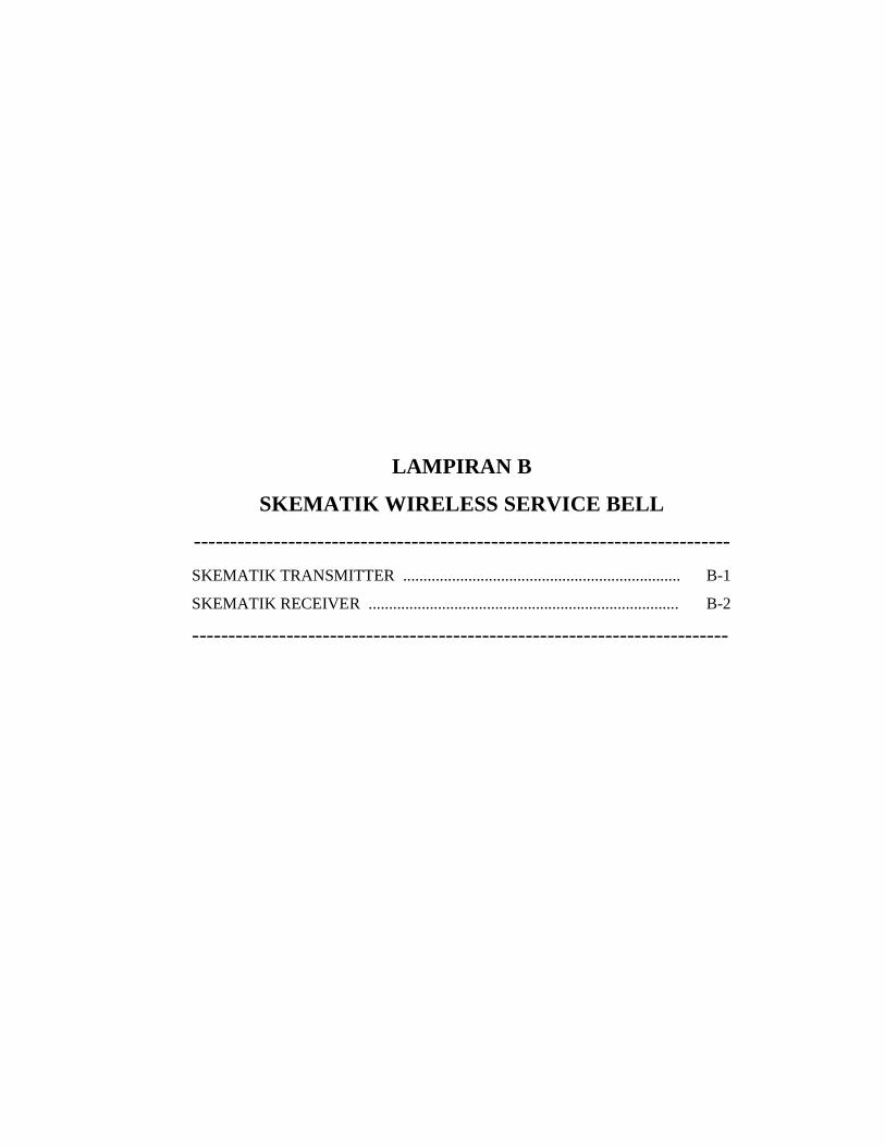
LAMPIRAN B
SKEMATIK WIRELESS SERVICE BELL
--------------------------------------------------------------------------
SKEMATIK TRANSMITTER .................................................................... B-1
SKEMATIK RECEIVER ............................................................................ B-2
--------------------------------------------------------------------------

SKEMATIK TRANSMITTER

SKEMATIK RECEIVER

LAMPIRAN C
PROGRAM PADA PENGONTROL MIKRO
ATMEGA16

/************************************************** *** This program was produced by the CodeWizardAVR V1.25.3 Professional Automatic Program Generator © Copyright 1998-2007 Pavel Haiduc, HP InfoTech s.r.l. http://www.hpinfotech.com
Project : Version : Date : 8/3/2010 Author : F4CG Company : F4CG Comments:
Chip type : ATmega16 Program type : Application Clock frequency : 11.059200 MHz Memory model : Small External SRAM size : 0 Data Stack size : 256 *************************************************** **/
#include <mega16.h> #include <delay.h>
// Alphanumeric LCD Module functions #asm .equ __lcd_port=0x15 ;PORTC #endasm #include <lcd.h>
#define RXB8 1 #define TXB8 0 #define UPE 2 #define OVR 3 #define FE 4 #define UDRE 5 #define RXC 7
#define FRAMING_ERROR (1<<FE) #define PARITY_ERROR (1<<UPE) #define DATA_OVERRUN (1<<OVR) #define DATA_REGISTER_EMPTY (1<<UDRE) #define RX_COMPLETE (1<<RXC)
// USART Receiver buffer #define RX_BUFFER_SIZE 8 char rx_buffer[RX_BUFFER_SIZE];

#if RX_BUFFER_SIZE<256 unsigned char rx_wr_index,rx_rd_index,rx_counter; #else unsigned int rx_wr_index,rx_rd_index,rx_counter; #endif
// This flag is set on USART Receiver buffer overflow bit rx_buffer_overflow;
// USART Receiver interrupt service routine interrupt [USART_RXC] void usart_rx_isr(void) char status,data; status=UCSRA; data=UDR; if ((status & (FRAMING_ERROR | PARITY_ERROR | DATA_OVERRUN))==0) rx_buffer[rx_wr_index]=data; if (++rx_wr_index == RX_BUFFER_SIZE) rx_wr_index=0; if (++rx_counter == RX_BUFFER_SIZE) rx_counter=0; rx_buffer_overflow=1; ; ; if(data=='R') /*program penanganan data interrupt yang diperoleh untuk mereset LCD*/ lcd_clear();
#ifndef _DEBUG_TERMINAL_IO_ // Get a character from the USART Receiver buffer #define _ALTERNATE_GETCHAR_ #pragma used+ char getchar(void) char data; while (rx_counter==0); data=rx_buffer[rx_rd_index]; if (++rx_rd_index == RX_BUFFER_SIZE) rx_rd_index=0; #asm("cli") --rx_counter; #asm("sei") return data; #pragma used- #endif
// Standard Input/Output functions

#include <stdio.h>
// Declare your global variables here
void main(void) // Declare your local variables here
// Input/Output Ports initialization // Port A initialization // Func7=In Func6=In Func5=In Func4=In Func3=In Func2=In Func1=In Func0=In // State7=T State6=T State5=T State4=T State3=T State2=T State1=T State0=T PORTA=0x00; DDRA=0x00;
// Port B initialization // Func7=Out Func6=Out Func5=Out Func4=Out Func3=Out Func2=Out Func1=Out Func0=Out // State7=0 State6=0 State5=0 State4=0 State3=0 State2=0 State1=0 State0=0 PORTB=0x00; DDRB=0xFF;
// Port C initialization // Func7=In Func6=In Func5=In Func4=In Func3=In Func2=In Func1=In Func0=In // State7=T State6=T State5=T State4=T State3=T State2=T State1=T State0=T PORTC=0x00; DDRC=0x00;
// Port D initialization // Func7=In Func6=In Func5=In Func4=In Func3=In Func2=In Func1=In Func0=In // State7=T State6=T State5=T State4=T State3=T State2=T State1=T State0=T PORTD=0x00; DDRD=0x00;
// Timer/Counter 0 initialization // Clock source: System Clock // Clock value: Timer 0 Stopped // Mode: Normal top=FFh // OC0 output: Disconnected TCCR0=0x00; TCNT0=0x00; OCR0=0x00;
// Timer/Counter 1 initialization // Clock source: System Clock // Clock value: Timer 1 Stopped // Mode: Normal top=FFFFh // OC1A output: Discon. // OC1B output: Discon. // Noise Canceler: Off

// Input Capture on Falling Edge // Timer 1 Overflow Interrupt: Off // Input Capture Interrupt: Off // Compare A Match Interrupt: Off // Compare B Match Interrupt: Off TCCR1A=0x00; TCCR1B=0x00; TCNT1H=0x00; TCNT1L=0x00; ICR1H=0x00; ICR1L=0x00; OCR1AH=0x00; OCR1AL=0x00; OCR1BH=0x00; OCR1BL=0x00;
// Timer/Counter 2 initialization // Clock source: System Clock // Clock value: Timer 2 Stopped // Mode: Normal top=FFh // OC2 output: Disconnected ASSR=0x00; TCCR2=0x00; TCNT2=0x00; OCR2=0x00;
// External Interrupt(s) initialization // INT0: Off // INT1: Off // INT2: Off MCUCR=0x00; MCUCSR=0x00;
// Timer(s)/Counter(s) Interrupt(s) initialization TIMSK=0x00;
// USART initialization // Communication Parameters: 8 Data, 1 Stop, No Parity // USART Receiver: On // USART Transmitter: On // USART Mode: Asynchronous // USART Baud rate: 9600 UCSRA=0x00; UCSRB=0x98; UCSRC=0x86; UBRRH=0x00; UBRRL=0x47;
// Analog Comparator initialization // Analog Comparator: Off

// Analog Comparator Input Capture by Timer/Counter 1: Off ACSR=0x80; SFIOR=0x00;
// LCD module initialization lcd_init(16);
// Global enable interrupts #asm("sei")
while (1)
PORTB=0B11111110; /*program pengolah data pada receiver*/ if(PINA.4==1) if(PINA.7==1) lcd_clear(); lcd_gotoxy(0,0); lcd_putsf("MEJA 1 BILL"); printf("MEJA 1 BILL "); if(PINA.4==1) if(PINA.6==1) lcd_clear(); lcd_gotoxy(0,0); lcd_putsf("MEJA 1 MENU"); printf("MEJA 1 MENU "); delay_ms(100); PORTB=0B11111101; if(PINA.4==1) if(PINA.7==1) lcd_clear(); lcd_gotoxy(0,0); lcd_putsf("MEJA 2 BILL"); printf("MEJA 2 BILL "); if(PINA.4==1) if(PINA.6==1) lcd_clear(); lcd_gotoxy(0,0); lcd_putsf("MEJA 2 MENU"); printf("MEJA 2 MENU "); delay_ms(100);
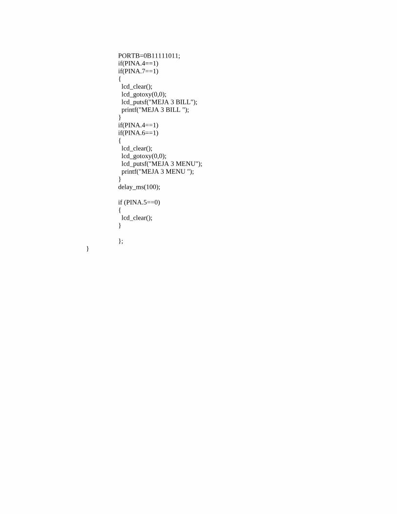
PORTB=0B11111011; if(PINA.4==1) if(PINA.7==1) lcd_clear(); lcd_gotoxy(0,0); lcd_putsf("MEJA 3 BILL"); printf("MEJA 3 BILL "); if(PINA.4==1) if(PINA.6==1) lcd_clear(); lcd_gotoxy(0,0); lcd_putsf("MEJA 3 MENU"); printf("MEJA 3 MENU "); delay_ms(100); if (PINA.5==0) lcd_clear(); ;

LAMPIRAN D
PROGRAM INTERFACING VB6

Dim x As String /*menetukan tipe data dari variabel x sebagai string*/
Private Sub Command1_Click() /*program penghentian sistem bila button exit di klik*/
MSComm1.PortOpen = False
Unload Me
End Sub
Private Sub Form_Load() /*program pengaktifan komunikasi serial*/
MSComm1.CommPort = 1
MSComm1.Settings = "9600,n,8,1"
MSComm1.PortOpen = True
List1.Clear
End Sub
Private Sub Image10_Click() /*program peresetan dan pengiriman interrupt ketika image10 diklik*/
Image3.Visible = False
Image2.Visible = False
Image1.Visible = True
Image10.Visible = False
Text4.Visible = False
Text5.Visible = False
Timer2.Enabled = False
Timer3.Enabled = False
MSComm1.Output = "R"
End Sub
Private Sub Image11_Click() /*program peresetan dan pengiriman interrupt ketika image11 diklik*/
Image5.Visible = False
Image6.Visible = False
Image4.Visible = True
Image11.Visible = False
Text6.Visible = False
Text7.Visible = False
Timer4.Enabled = False
Timer5.Enabled = False

MSComm1.Output = "R"
End Sub
Private Sub Image12_Click() /*program peresetan dan pengiriman interrupt ketika image12 diklik*/
Image8.Visible = False
Image9.Visible = False
Image7.Visible = True
Image12.Visible = False
Text8.Visible = False
Text9.Visible = False
Timer6.Enabled = False
Timer7.Enabled = False
MSComm1.Output = "R"
End Sub
Private Sub Timer1_Timer() /*program penerimaan, pengecekan data, & pengaturan tampilannya*/
x = MSComm1.Input
If Len(x) > 0 Then
If Left(x, 11) = "MEJA 1 BILL" Then
Image2.Visible = True
Image1.Visible = False
Timer2.Enabled = True
Image10.Visible = True
Text4.Visible = True
Text5.Visible = False
End If
If Left(x, 11) = "MEJA 1 MENU" Then
Image2.Visible = True
Image1.Visible = False
Timer2.Enabled = True
Image10.Visible = True
Text5.Visible = True
Text4.Visible = False
End If

If Left(x, 11) = "MEJA 2 BILL" Then
Image5.Visible = True
Image4.Visible = False
Timer4.Enabled = True
Image11.Visible = True
Text6.Visible = True
Text7.Visible = False
End If
If Left(x, 11) = "MEJA 2 MENU" Then
Image5.Visible = True
Image4.Visible = False
Timer4.Enabled = True
Image11.Visible = True
Text7.Visible = True
Text6.Visible = False
End If
If Left(x, 11) = "MEJA 3 BILL" Then
Image8.Visible = True
Image7.Visible = False
Timer6.Enabled = True
Image12.Visible = True
Text8.Visible = True
Text9.Visible = False
End If
If Left(x, 11) = "MEJA 3 MENU" Then
Image8.Visible = True
Image7.Visible = False
Timer6.Enabled = True
Image12.Visible = True
Text9.Visible = True
Text8.Visible = False
End If
List1.AddItem (x & Format$(Time, "hh:mm:ss AM/PM"))
End If

End Sub
Private Sub Timer2_Timer() /*program membuat image3 berkedip dengan selang waktu tertentu*/
Image3.Visible = True
Timer2.Enabled = False
Timer3.Enabled = True
End Sub
Private Sub Timer3_Timer()
Image3.Visible = False
Timer2.Enabled = True
Timer3.Enabled = False
End Sub
Private Sub Timer4_Timer() /*program membuat image6 berkedip dengan selang waktu tertentu*/
Image6.Visible = True
Timer4.Enabled = False
Timer5.Enabled = True
End Sub
Private Sub Timer5_Timer()
Image6.Visible = False
Timer5.Enabled = False
Timer4.Enabled = True
End Sub
Private Sub Timer6_Timer() /*program membuat image9 berkedip dengan selang waktu tertentu*/
Image9.Visible = True
Timer6.Enabled = False
Timer7.Enabled = True
End Sub
Private Sub Timer7_Timer()
Image9.Visible = False
Timer7.Enabled = False
Timer6.Enabled = True
End Sub

LAMPIRAN E
DATASHEET
--------------------------------------------------------------------------
IC HT12D (DECODER) ............................................................................ E-1
IC HT12E (ENCODER) ............................................................................. E-10
MODUL RF TLP-RLP 315 ........................................................................ E-23
IC 74LS04 (INVERTER) ........................................................................... E-24
IC NE555 (CLOCK) .................................................................................. E-26
IC MAX232 (TRANSCEIVER) ................................................................ E-36
--------------------------------------------------------------------------

212
Series of Decoders
Selection Table
Function Address
No.
DataVT Oscillator Trigger Package
Part No. No. Type
HT12D 8 4 L Ö RC oscillator DIN active ²Hi² 18 DIP/20 SOP
HT12F 12 0 ¾ Ö RC oscillator DIN active ²Hi² 18 DIP/20 SOP
Notes: Data type: L stands for latch type data output.
VT can be used as a momentary data output.
1 July 12, 1999
General Description
The 212
decoders are a series of CMOS LSIs for
remote control system applications. They are
paired with Holtek¢s 212
series of encoders (re-
fer to the encoder/decoder cross reference ta-
ble). For proper operation, a pair of
encoder/decoder with the same number of ad-
dresses and data format should be chosen.
The decoders receive serial addresses and data
from a programmed 212
series of encoders that
are transmitted by a carrier using an RF or an
IR transmission medium. They compare the se-
rial input data three times continuously with
their local addresses. If no error or unmatched
codes are found, the input data codes are de-
coded and then transferred to the output pins.
The VT pin also goes high to indicate a valid
transmission.
The 212
series of decoders are capable of decod-
ing informations that consist of N bits of ad-
dress and 12-N bits of data. Of this series, the
HT12D is arranged to provide 8 address bits
and 4 data bits, and HT12F is used to decode 12
bits of address information.
Features
· Operating voltage: 2.4V~12V
· Low power and high noise immunity CMOS
technology
· Low standby current
· Capable of decoding 12 bits of information
· Pair with Holtek¢s 212
series of encoders
· Binary address setting
· Received codes are checked 3 times
· Address/Data number combination- HT12D: 8 address bits and 4 data bits- HT12F: 12 address bits only
· Built-in oscillator needs only 5% resistor
· Valid transmission indicator
· Easy interface with an RF or an infrared
transmission medium
· Minimal external components
Applications
· Burglar alarm system
· Smoke and fire alarm system
· Garage door controllers
· Car door controllers
· Car alarm system
· Security system
· Cordless telephones
· Other remote control systems

Block Diagram
Note: The address/data pins are available in various combinations (see the address/data table).
Pin Assignment
212
Series of Decoders
2 July 12, 1999
D a t a S h i f t R e g i s t e r
O s c i l l a t o r
B u f f e r
S y n c . D e t e c t o r
D i v i d e r
C o m p a r a t o r C o m p a r a t o r
B u f f e r T r a n s m i s s i o n G a t e C i r c u i t
D a t a D e t e c t o r
C o n t r o l L o g i c
O S C 1O S C 2
D I N
V D D V S S
V T
D a t a L a t c h C i r c u i t
A d d r e s s
8 - A d d r e s s4 - D a t a
1 2 - A d d r e s s 0 - D a t a
A 0
A 1
A 2
A 3
A 4
A 5
A 6
A 7
V S S
V D D
V T
O S C 1
O S C 2
D I N
D 1 1
D 1 0
D 9
D 8
1
2
3
4
5
6
7
8
9
1 8
1 7
1 6
1 5
1 4
1 3
1 2
1 1
1 0
1 2 - A d d r e s s 0 - D a t a
A 0
A 1
A 2
A 3
A 4
A 5
A 6
A 7
V S S
V D D
V T
O S C 1
O S C 2
D I N
A 1 1
A 1 0
A 9
A 8
1
2
3
4
5
6
7
8
9
1 8
1 7
1 6
1 5
1 4
1 3
1 2
1 1
1 0
1
2
3
4
5
6
7
8
9
1 0
2 0
1 9
1 8
1 7
1 6
1 5
1 4
1 3
1 2
1 1
N C
V D D
V T
O S C 1
O S C 2
D I N
A 1 1
A 1 0
A 9
A 8
N C
A 0
A 1
A 2
A 3
A 4
A 5
A 6
A 7
V S S
8 - A d d r e s s4 - D a t a
1
2
3
4
5
6
7
8
9
1 0
2 0
1 9
1 8
1 7
1 6
1 5
1 4
1 3
1 2
1 1
N C
V D D
V T
O S C 1
O S C 2
D I N
D 1 1
D 1 0
D 9
D 8
N C
A 0
A 1
A 2
A 3
A 4
A 5
A 6
A 7
V S S
H T 1 2 F 2 0 S O P
H T 1 2 F 1 8 D I P
H T 1 2 D 1 8 D I P
H T 1 2 D 2 0 S O P

Pin Description
Pin Name I/OInternal
ConnectionDescription
A0~A11 I
NMOS
TRANSMISSION
GATE
Input pins for address A0~A11 setting
They can be externally set to VDD or VSS.
D8~D11 O CMOS OUT Output data pins
DIN I CMOS IN Serial data input pin
VT O CMOS OUT Valid transmission, active high
OSC1 I OSCILLATOR Oscillator input pin
OSC2 O OSCILLATOR Oscillator output pin
VSS I ¾ Negative power supply (GND)
VDD I ¾ Positive power supply
Approximate internal connection circuits
Absolute Maximum Ratings
Supply Voltage...............................-0.3V to 13V Storage Temperature.................-50°C to 125°C
Input Voltage....................VSS-0.3 to VDD+0.3V Operating Temperature ..............-20°C to 75°C
Note: These are stress ratings only. Stresses exceeding the range specified under ²Absolute Maxi-
mum Ratings² may cause substantial damage to the device. Functional operation of this de-
vice at other conditions beyond those listed in the specification is not implied and prolonged
exposure to extreme conditions may affect device reliability.
212
Series of Decoders
3 July 12, 1999
N M O ST R A N S M I S S I O N
G A T E
C M O S I N O S C I L L A T O R
O S C 1 O S C 2
C M O S O U T
E N

Electrical Characteristics Ta=25°C
Symbol ParameterTest Conditions
Min. Typ. Max. UnitVDD Conditions
VDD Operating Voltage ¾ ¾ 2.4 5 12 V
ISTB Standby Current5V
Oscillator stops¾ 0.1 1 mA
12V ¾ 2 4 mA
IDD Operating Current 5VNo load
fOSC=150kHz¾ 200 400 mA
IO
Data Output Source
Current (D8~D11)5V VOH=4.5V -1 -1.6 ¾ mA
Data Output Sink
Current (D8~D11)5V VOL=0.5V 1 1.6 ¾ mA
IVT
VT Output Source Current5V
VOH=4.5V -1 -1.6 ¾ mA
VT Output Sink Current VOL=0.5V 1 1.6 ¾ mA
VIH ²H² Input Voltage 5V ¾ 3.5 ¾ 5 V
VIL ²L² Input Voltage 5V ¾ 0 ¾ 1 V
fOSC Oscillator Frequency 5V ROSC=51kW ¾ 150 ¾ kHz
212
Series of Decoders
4 July 12, 1999

212
Series of Decoders
5 July 12, 1999
Functional Description
Operation
The 212
series of decoders provides various com-
binations of addresses and data pins in differ-
ent packages so as to pair with the 212
series of
encoders.
The decoders receive data that are transmitted
by an encoder and interpret the first N bits of
code period as addresses and the last 12-N bits
as data, where N is the address code number. A
signal on the DIN pin activates the oscillator
which in turn decodes the incoming address
and data. The decoders will then check the re-
ceived address three times continuously. If the
received address codes all match the contents of
the decoder¢s local address, the 12-N bits of
data are decoded to activate the output pins
and the VT pin is set high to indicate a valid
transmission. This will last unless the address
code is incorrect or no signal is received.
The output of the VT pin is high only when the
transmission is valid. Otherwise it is always
low.
Output type
Of the 212
series of decoders, the HT12F has no
data output pin but its VT pin can be used as a
momentary data output. The HT12D, on the
other hand, provides 4 latch type data pins
whose data remain unchanged until new data
are received.
Part
No.
Data
Pins
Address
Pins
Output
Type
Operating
Voltage
HT12D 4 8 Latch 2.4V~12V
HT12F 0 12 ¾ 2.4V~12V
Flowchart
The oscillator is disabled in the standby state
and activated when a logic ²high² signal applies
to the DIN pin. That is to say, the DIN should be
kept low if there is no signal input.
Y e s
C o d e i n ?
S t o r e d a t a
N o
Y e s
N o
N o
N o
Y e s
S t a n d b y m o d e
D i s a b l e V T &i g n o r e t h e r e s t o f
t h i s w o r d
Y e s
N o
Y e s
A d d r e s s o rd a t a e r r o r ?
L a t c h d a t a t o o u t p u t &a c t i v a t e V T
A d d r e s s b i t sm a t c h e d ?
M a t c hp r e v i o u s s t o r e d
d a t a ?
P o w e r o n
3 t i m e so f c h e c k i n gc o m p l e t e d ?

Decoder timing
Encoder/Decoder cross reference table
Decoders
Part No.Data Pins Address Pins VT Pair Encoder
Package
Encoder Decoder
DIP SOP DIP SOP
HT12D 4 8 ÖHT12A 18 20
18 20HT12E 18 20
HT12F 0 12 ÖHT12A 18 20
18 20HT12E 18 20
Address/Data sequence
The following table provides address/data sequence for various models of the 212
series of decoders. A
correct device should be chosen according to the requirements of the individual addresses and data.
Part No.Address/Data Bits
0 1 2 3 4 5 6 7 8 9 10 11
HT12D A0 A1 A2 A3 A4 A5 A6 A7 D8 D9 D10 D11
HT12F A0 A1 A2 A3 A4 A5 A6 A7 A8 A9 A10 A11
212
Series of Decoders
6 July 12, 1999
2 c l o c k s1 4
c h e c k
4 w o r d s 4 w o r d s
E n c o d e rD O U T
T r a n s m i t t e dC o n t i n u o u s l y
< 1 w o r d
E n c o d e rT r a n s m i s s i o n
E n a b l e
c h e c k
D e c o d e r V T
L a t c h e dD a t a O u t
2 c l o c k s1 4

Oscillator frequency vs supply voltage
The recommended oscillator frequency is fOSCD (decoder) @ 50 fOSCE (HT12E encoder)
@1
3fOSCE (HT12A encoder).
212
Series of Decoders
7 July 12, 1999
f o s c( S c a l e )
R o s c ( W )
0 . 5 0
( 1 0 0 k H z ) 1 . 0 0
1 . 5 0
2 . 0 0
2 . 5 0
3 . 5 0
4 . 0 0
3 . 0 0
0 . 2 5
2 3 4 5 6 7 8 9 1 0 1 1 1 2 1 3 V D D ( V D C )
6 8 k
6 2 k
5 6 k
5 1 k
4 7 k
4 3 k
3 9 k
3 6 k
3 3 k
3 0 k
2 7 k
7 5 k
8 2 k
1 0 0 k
1 2 0 k
1 5 0 k
1 8 0 k
2 2 0 k

Application Circuits
Notes: Typical infrared receiver: PIC-12043T/PIC-12043S (KODESHI CORP.)
or LTM9052 (LITEON CORP.)
Typical RF receiver: JR-200 (JUWA CORP.)
RE-99 (MING MICROSYSTEM, U.S.A.)
212
Series of Decoders
8 July 12, 1999
R e c e i v e r C i r c u i t
H T 1 2 D
A 0
A 1
A 2
A 3
A 4
A 5
A 6
A 7
V S S
V D D
V T
O S C 1
O S C 2
D I N
D 1 1
D 1 0
D 9
D 8
1
2
3
4
5
6
7
8
9
1 8
1 7
1 6
1 5
1 4
1 3
1 2
1 1
1 0
R O S C
V D D
R e c e i v e r C i r c u i t
H T 1 2 F
A 0
A 1
A 2
A 3
A 4
A 5
A 6
A 7
V S S
V D D
V T
O S C 1
O S C 2
D I N
A 1 1
A 1 0
A 9
A 8
1
2
3
4
5
6
7
8
9
1 8
1 7
1 6
1 5
1 4
1 3
1 2
1 1
1 0
R O S C
V D D

212
Series of Decoders
9 July 12, 1999
Copyright ã 1999 by HOLTEK SEMICONDUCTOR INC.
The information appearing in this Data Sheet is believed to be accurate at the time of publication. However, Holtekassumes no responsibility arising from the use of the specifications described. The applications mentioned herein areused solely for the purpose of illustration and Holtek makes no warranty or representation that such applicationswill be suitable without further modification, nor recommends the use of its products for application that may pres-ent a risk to human life due to malfunction or otherwise. Holtek reserves the right to alter its products without priornotification. For the most up-to-date information, please visit our web site at http://www.holtek.com.tw.
Holtek Semiconductor Inc. (Headquarters)No.3 Creation Rd. II, Science-based Industrial Park, Hsinchu, Taiwan, R.O.C.Tel: 886-3-563-1999Fax: 886-3-563-1189
Holtek Semiconductor Inc. (Taipei Office)5F, No.576, Sec.7 Chung Hsiao E. Rd., Taipei, Taiwan, R.O.C.Tel: 886-2-2782-9635Fax: 886-2-2782-9636Fax: 886-2-2782-7128 (International sales hotline)
Holtek Microelectronics Enterprises Ltd.RM.711, Tower 2, Cheung Sha Wan Plaza, 833 Cheung Sha Wan Rd., Kowloon, Hong KongTel: 852-2-745-8288Fax: 852-2-742-8657

This datasheet has been downloaded from:
www.DatasheetCatalog.com
Datasheets for electronic components.
HT12A/HT12E
212
Series of Encoders
Selection Table
Function Address
No.
Address/
Data No.
Data
No.Oscillator Trigger Package
Carrier
Output
Negative
PolarityPart No.
HT12A 8 0 4455kHz
resonatorD8~D11
18 DIP
20 SOP38kHz No
HT12E 8 4 0RC
oscillatorTE
18 DIP
20 SOPNo No
Note: Address/Data represents pins that can be address or data according to the decoder require-
ment.
1 April 11, 2000
General Description
The 212 encoders are a series of CMOS LSIs for
remote control system applications. They are
capable of encoding information which consists
of N address bits and 12N data bits. Each ad-
dress/data input can be set to one of the two
logic states. The programmed addresses/data
are transmitted together with the header bits
via an RF or an infrared transmission medium
upon receipt of a trigger signal. The capability
to select a TE trigger on the HT12E or a DATA
trigger on the HT12A further enhances the ap-
plication flexibility of the 212 series of encoders.
The HT12A additionally provides a 38kHz car-
rier for infrared systems.
Features
Operating voltage 2.4V~5V for the HT12A 2.4V~12V for the HT12E
Low power and high noise immunity CMOS
technology
Low standby current: 0.1A (typ.) at
VDD=5V
HT12A with a 38kHz carrier for infrared
transmission medium
Minimum transmission word Four words for the HT12E One word for the HT12A
Built-in oscillator needs only 5% resistor
Data code has positive polarity
Minimal external components
HT12A/E: 18-pin DIP/20-pin SOP package
Applications
Burglar alarm system
Smoke and fire alarm system
Garage door controllers
Car door controllers
Car alarm system
Security system
Cordless telephones
Other remote control systems

Block Diagram
TE trigger
HT12E
DATA trigger
HT12A
Note: The address data pins are available in various combinations (refer to the address/data table).
HT12A/HT12E
2 April 11, 2000
!
"
#
$
% ! &
"
#
' ( )
* *
!
$
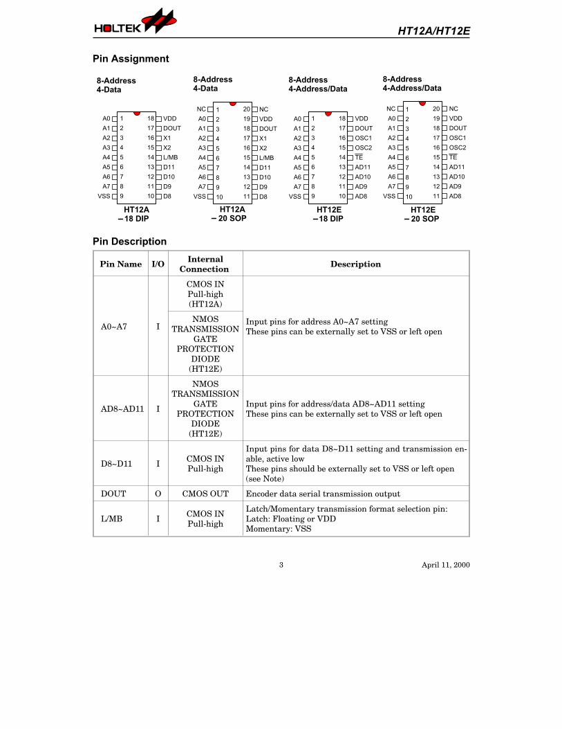
Pin Assignment
Pin Description
Pin Name I/OInternal
ConnectionDescription
A0~A7 I
CMOS IN
Pull-high
(HT12A)
Input pins for address A0~A7 setting
These pins can be externally set to VSS or left open
NMOS
TRANSMISSION
GATE
PROTECTION
DIODE
(HT12E)
AD8~AD11 I
NMOS
TRANSMISSION
GATE
PROTECTION
DIODE
(HT12E)
Input pins for address/data AD8~AD11 setting
These pins can be externally set to VSS or left open
D8~D11 ICMOS IN
Pull-high
Input pins for data D8~D11 setting and transmission en-
able, active low
These pins should be externally set to VSS or left open
(see Note)
DOUT O CMOS OUT Encoder data serial transmission output
L/MB ICMOS IN
Pull-high
Latch/Momentary transmission format selection pin:
Latch: Floating or VDD
Momentary: VSS
HT12A/HT12E
3 April 11, 2000
+
%
&
!
"
*
*
' ( )
,
$
+
%
&
!
$
,
$
!
&
%
+
+
%
&
!
$
,
,
$
!
&
%
+
-
"
*
*
' ( )
,
$
-
+
%
&
!
+
%
&
!
"
,
$
+
%
&
!
$
,
$
!
&
%
+
+
%
&
!
$
,
,
$
!
&
%
+
-
"
,
$
-
+
%
&
!

Pin Name I/OInternal
ConnectionDescription
TE ICMOS IN
Pull-highTransmission enable, active low (see Note)
OSC1 I OSCILLATOR 1 Oscillator input pin
OSC2 O OSCILLATOR 1 Oscillator output pin
X1 I OSCILLATOR 2 455kHz resonator oscillator input
X2 O OSCILLATOR 2 455kHz resonator oscillator output
VSS I Negative power supply, grounds
VDD I Positive power supply
Note: D8~D11 are all data input and transmission enable pins of the HT12A.
TE is a transmission enable pin of the HT12E.
Approximate internal connections
Absolute Maximum Ratings
Supply Voltage (HT12A) ..............0.3V to 5.5V Supply Voltage (HT12E) ...............0.3V to 13V
Input Voltage....................VSS0.3 to VDD+0.3V Storage Temperature.................50C to 125C
Operating Temperature...............20C to 75C
Note: These are stress ratings only. Stresses exceeding the range specified under Absolute Maxi-
mum Ratings may cause substantial damage to the device. Functional operation of this device
at other conditions beyond those listed in the specification is not implied and prolonged expo-
sure to extreme conditions may affect device reliability.
HT12A/HT12E
4 April 11, 2000
- ) . - ) / / -
) / -0 1 2 3 2
) " / ' ' .
/ ' ' .
* *
-
- ) . - ) / / - 0 . / - /

Electrical Characteristics
HT12A Ta=25C
Symbol ParameterTest Conditions
Min. Typ. Max. UnitVDD Conditions
VDD Operating Voltage 2.4 3 5 V
ISTB Standby Current3V
Oscillator stops 0.1 1 A
5V 0.1 1 A
IDD Operating Current3V No load
fOSC=455kHz
200 400 A
5V 400 800 A
IDOUT Output Drive Current 5VVOH=0.9VDD (Source) 1 1.6 mA
VOL=0.1VDD (Sink) 2 3.2 mA
VIH H Input Voltage 0.8VDD VDD V
VIL L Input Voltage 0 0.2VDD V
RDATAD8~D11 Pull-high
Resistance5V VDATA=0V 150 300 k
HT12E Ta=25C
Symbol ParameterTest Conditions
Min. Typ. Max. UnitVDD Conditions
VDD Operating Voltage 2.4 5 12 V
ISTB Standby Current3V
Oscillator stops 0.1 1 A
12V 2 4 A
IDD Operating Current3V No load
fOSC=3kHz
40 80 A
12V 150 300 A
IDOUT Output Drive Current 5VVOH=0.9VDD (Source) 1 1.6 mA
VOL=0.1VDD (Sink) 1 1.6 mA
VIH H Input Voltage 0.8VDD VDD V
VIL L Input Voltage 0 0.2VDD V
fOSC Oscillator Frequency 5V ROSC=1.1M 3 kHz
RTE TE Pull-high Resistance 5V VTE=0V 1.5 3 M
HT12A/HT12E
5 April 11, 2000

Functional Description
Operation
The 212 series of encoders begin a 4-word transmission cycle upon receipt of a transmission enable
(TE for the HT12E or D8~D11 for the HT12A, active low). This cycle will repeat itself as long as the
transmission enable (TE or D8~D11) is held low. Once the transmission enable returns high the en-
coder output completes its final cycle and then stops as shown below.
HT12A/HT12E
6 April 11, 2000
+ 4 + 4
"
5 4
Transmission timing for the HT12E
"
5 4
$ 6 7 1
4
4 2 $ 8 9 :
4
Transmission timing for the HT12A (L/MB=Floating or VDD)
"
$ 6 7 1
4
5 4
! 4
4
! 4
; < =
; < =
Transmission timing for the HT12A (L/MB=VSS)

Information word
If L/MB=1 the device is in the latch mode (for use with the latch type of data decoders). When the trans-
mission enable is removed during a transmission, the DOUT pin outputs a complete word and then
stops. On the other hand, if L/MB=0 the device is in the momentary mode (for use with the momentary
type of data decoders). When the transmission enable is removed during a transmission, the DOUT
outputs a complete word and then adds 7 words all with the 1 data code.
An information word consists of 4 periods as illustrated below.
Address/data waveform
Each programmable address/data pin can be externally set to one of the following two logic states as
shown below.
HT12A/HT12E
7 April 11, 2000
( > # ?
? ? ; > = ? ?
Composition of information
@ @
@ A @
(
Address/Data bit waveform for the HT12E
@ @
@ A @
@ @
@ A @
$ 8 9 :
Address/Data bit waveform for the HT12A

The address/data bits of the HT12A are transmitted with a 38kHz carrier for infrared remote con-
troller flexibility.
Address/data programming (preset)
The status of each address/data pin can be individually pre-set to logic high or low. If a transmis-
sion-enable signal is applied, the encoder scans and transmits the status of the 12 bits of ad-
dress/data serially in the order A0 to AD11 for the HT12E encoder and A0 to D11 for the HT12A
encoder.
During information transmission these bits are transmitted with a preceding synchronization bit. If
the trigger signal is not applied, the chip enters the standby mode and consumes a reduced current of
less than 1A for a supply voltage of 5V.
Usual applications preset the address pins with individual security codes using DIP switches or PCB
wiring, while the data is selected by push buttons or electronic switches.
The following figure shows an application using the HT12E:
The transmitted information is as shown:
Pilot
&
Sync.
A0
1
A1
0
A2
1
A3
0
A4
0
A5
0
A6
1
A7
1
AD8
1
AD9
1
AD10
1
AD11
0
HT12A/HT12E
8 April 11, 2000
+ % & ! $ ,
"

Address/Data sequence
The following provides the address/data sequence table for various models of the 212 series of
encoders. The correct device should be selected according to the individual address and data require-
ments.
Part No.Address/Data Bits
0 1 2 3 4 5 6 7 8 9 10 11
HT12A A0 A1 A2 A3 A4 A5 A6 A7 D8 D9 D10 D11
HT12E A0 A1 A2 A3 A4 A5 A6 A7 AD8 AD9 AD10 AD11
Transmission enable
For the HT12E encoders, transmission is enabled by applying a low signal to the TE pin. For the
HT12A encoders, transmission is enabled by applying a low signal to one of the data pins D8~D11.
Two erroneous HT12E application circuits
The HT12E must follow closely the application circuits provided by Holtek (see the Application cir-
cuits).
Error: AD8~AD11 pins input voltage > VDD+0.3V
HT12A/HT12E
9 April 11, 2000
,
$

Error: The ICs power source is activated by pins AD8~AD11
Flowchart
HT12A HT12E
Note: D8~D11 are transmission enables of the HT12A.
TE is the transmission enable of the HT12E.
HT12A/HT12E
10 April 11, 2000
,
$
>
> B-
-
4 2 ?
> B
' ( ) < - B
2
-
C
C
C
! 2
0 4
>
> B
-
-
C
C
+ 4
>
+ 4
0 4

Oscillator frequency vs supply voltage
The recommended oscillator frequency is fOSCD (decoder) 50 fOSCE (HT12E encoder)
1
3fOSCE (HT12A encoder)
HT12A/HT12E
11 April 11, 2000
+ % & ! $ ,
#
#
; 8 9 : = #
+ #
% #
& #
! #
# )
# % )
# )
# )
, 8
$ 8
! % 8
& $ 8
& 8
% & 8
% 8
+ ! 8

Application Circuits
Note: Typical infrared diode: EL-1L2 (KODENSHI CORP.)
Typical RF transmitter: JR-220 (JUWA CORP.)
HT12A/HT12E
12 April 11, 2000
+ % % 8
)
? D
? D
$ %
+
%
&
!
$
,
+
%
&
!
"
*
*
' ( )
,
$
$
!
&
%
+
8
+
%
&
!
"
,
$
+
%
&
!
$
,
$
!
&
%
+
.

HT12A/HT12E
13 April 11, 2000
Copyright 2000 by HOLTEK SEMICONDUCTOR INC.
The information appearing in this Data Sheet is believed to be accurate at the time of publication. However, Holtekassumes no responsibility arising from the use of the specifications described. The applications mentioned herein areused solely for the purpose of illustration and Holtek makes no warranty or representation that such applicationswill be suitable without further modification, nor recommends the use of its products for application that may pres-ent a risk to human life due to malfunction or otherwise. Holtek reserves the right to alter its products without priornotification. For the most up-to-date information, please visit our web site at http://www.holtek.com.tw.
Holtek Semiconductor Inc. (Headquarters)No.3 Creation Rd. II, Science-based Industrial Park, Hsinchu, Taiwan, R.O.C.Tel: 886-3-563-1999Fax: 886-3-563-1189
Holtek Semiconductor Inc. (Taipei Office)5F, No.576, Sec.7 Chung Hsiao E. Rd., Taipei, Taiwan, R.O.C.Tel: 886-2-2782-9635Fax: 886-2-2782-9636Fax: 886-2-2782-7128 (International sales hotline)
Holtek Semiconductor (Hong Kong) Ltd.RM.711, Tower 2, Cheung Sha Wan Plaza, 833 Cheung Sha Wan Rd., Kowloon, Hong KongTel: 852-2-745-8288Fax: 852-2-742-8657
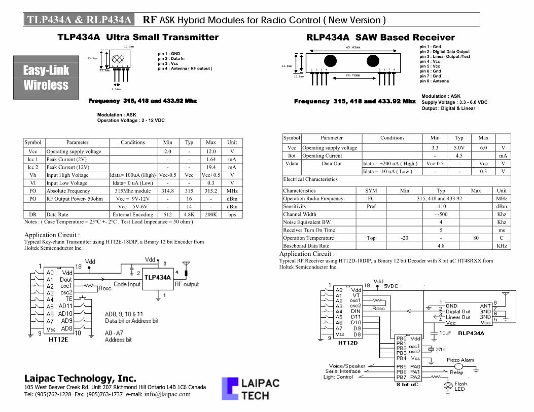
TLP434A & RLP434A RF ASK Hybrid Modules for Radio Control ( New Version )
Laipac Technology, Inc.105 West Beaver Creek Rd. Unit 207 Richmond Hill Ontario L4B 1C6 Canada
Tel: (905)762-1228 Fax: (905)763-1737 e-mail: [email protected]
Symbol Parameter Conditions Min Typ Max Unit
Vcc Operating supply voltage 2.0 - 12.0 V
Icc 1 Peak Current (2V) - - 1.64 mA
Icc 2 Peak Current (12V) - - 19.4 mA
Vh Input High Voltage Idata= 100uA (High) Vcc-0.5 Vcc Vcc+0.5 V
Vl Input Low Voltage Idata= 0 uA (Low) - - 0.3 V
FO Absolute Frequency 315Mhz module 314.8 315 315.2 MHz
PO RF Output Power- 50ohm Vcc = 9V-12V - 16 - dBm
Vcc = 5V-6V - 14 - dBm
DR Data Rate External Encoding 512 4.8K 200K bps
Notes : ( Case Temperature = 25°C +- 2°C , Test Load Impedance = 50 ohm )
Application Circuit : Typical Key-chain Transmitter using HT12E-18DIP, a Binary 12 bit Encoder from
Holtek Semiconductor Inc. Application Circuit : Typical RF Receiver using HT12D-18DIP, a Binary 12 bit Decoder with 8 bit uC HT48RXX from
Holtek Semiconductor Inc.
Easy-Link
Wireless
Symbol Parameter Conditions Min Typ Max
Vcc Operating supply voltage 3.3 5.0V 6.0 V
Itot Operating Current - 4.5 mA
Idata = +200 uA ( High ) Vcc-0.5 - Vcc V Vdata Data Out
Idata = -10 uA ( Low ) - - 0.3 V
Electrical Characteristics
Characteristics SYM Min Typ Max Unit
Operation Radio Frequency FC 315, 418 and 433.92 MHz
Sensitivity Pref -110 dBm
Channel Width +-500 Khz
Noise Equivalent BW 4 Khz
Receiver Turn On Time 5 ms
Operation Temperature Top -20 - 80 C
Baseboard Data Rate 4.8 KHz
TLP434A Ultra Small Transmitter
1 2 3 4
13.0mm
13.3mm
2.54mm
pin 1 : GND
pin 2 : Data In
pin 3 : Vcc
pin 4 : Antenna ( RF output )
Frequency 315, 418 and 433.92 Mhz Frequency 315, 418 and 433.92 Mhz Frequency 315, 418 and 433.92 Mhz Frequency 315, 418 and 433.92 Mhz
Modulation : ASKOperation Voltage : 2 - 12 VDC
24.72mm
43.42mm
1 2 3 4
3 4
5 6 7 8
7 8
10.5mm
11.5mm
pin 1 : Gnd
pin 2 : Digital Data Output
pin 3 : Linear Output /Test
pin 4 : Vcc
pin 5 : Vcc
pin 6 : Gnd
pin 7 : Gnd
pin 8 : Antenna
FrequencyFrequency Frequency Frequency 315, 418 and 433.92 Mhz315, 418 and 433.92 Mhz315, 418 and 433.92 Mhz315, 418 and 433.92 MhzModulation : ASK
Supply Voltage : 3.3 - 6.0 VDC
Output : Digital & Linear
RLP434A SAW Based Receiver10.3mm

5-1
FAST AND LS TTL DATA
HEX INVERTER
14 13 12 11 10 9
1 2 3 4 5 6
VCC
8
7
GND
GUARANTEED OPERATING RANGES
Symbol Parameter Min Typ Max Unit
VCC Supply Voltage 54
74
4.5
4.75
5.0
5.0
5.5
5.25
V
TA Operating Ambient Temperature Range 54
74
–55
0
25
25
125
70
°C
IOH Output Current — High 54, 74 –0.4 mA
IOL Output Current — Low 54
74
4.0
8.0
mA
SN54/74LS04
HEX INVERTER
LOW POWER SCHOTTKY
J SUFFIX
CERAMIC
CASE 632-08
N SUFFIX
PLASTIC
CASE 646-06
141
14
1
ORDERING INFORMATION
SN54LSXXJ Ceramic
SN74LSXXN Plastic
SN74LSXXD SOIC
14
1
D SUFFIX
SOIC
CASE 751A-02

5-2
FAST AND LS TTL DATA
SN54/74LS04
DC CHARACTERISTICS OVER OPERATING TEMPERATURE RANGE (unless otherwise specified)
Limits
Symbol Parameter Min Typ Max Unit Test Conditions
VIH Input HIGH Voltage 2.0 VGuaranteed Input HIGH Voltage for
All Inputs
VIL Input LOW Voltage54 0.7
VGuaranteed Input LOW Voltage for
VIL Input LOW Voltage74 0.8
Vp g
All Inputs
VIK Input Clamp Diode Voltage –0.65 –1.5 V VCC = MIN, IIN = –18 mA
VOH Output HIGH Voltage54 2.5 3.5 V VCC = MIN, IOH = MAX, VIN = VIH
VOH Output HIGH Voltage74 2.7 3.5 V
CC , OH , IN IHor VIL per Truth Table
VOL Output LOW Voltage54, 74 0.25 0.4 V IOL = 4.0 mA VCC = VCC MIN,
VIN = VIL or VIHVOL Output LOW Voltage74 0.35 0.5 V IOL = 8.0 mA
VIN = VIL or VIHper Truth Table
IIH Input HIGH Current20 µA VCC = MAX, VIN = 2.7 V
IIH Input HIGH Current0.1 mA VCC = MAX, VIN = 7.0 V
IIL Input LOW Current –0.4 mA VCC = MAX, VIN = 0.4 V
IOS Short Circuit Current (Note 1) –20 –100 mA VCC = MAX
ICC
Power Supply Current
Total, Output HIGH 2.4 mA VCC = MAXICCTotal, Output LOW 6.6
mA VCC MAX
Note 1: Not more than one output should be shorted at a time, nor for more than 1 second.
AC CHARACTERISTICS (TA = 25°C)
Limits
Symbol Parameter Min Typ Max Unit Test Conditions
tPLH Turn-Off Delay, Input to Output 9.0 15 ns VCC = 5.0 V
tPHL Turn-On Delay, Input to Output 10 15 ns
CCCL = 15 pF

July 1998
NDIP8
(Plastic Package)
DSO8
(Plastic Micropackage)
1
2
3
4 5
6
7
8 1 - GND
2 - Trigger3 - Output
4 - Reset
5 - Control voltage
6 - Threshold
7 - Discharge
8 - VCC
PIN CONNECTIONS (top view)
. LOW TURN OFF TIME.MAXIMUM OPERATING FREQUENCYGREATERTHAN 500kHz. TIMING FROMMICROSECONDS TO HOURS.OPERATES IN BOTH ASTABLE ANDMONOSTABLEMODES. HIGH OUTPUT CURRENT CAN SOURCE ORSINK 200mA. ADJUSTABLE DUTY CYCLE. TTL COMPATIBLE. TEMPERATURE STABILITY OF 0.005%PERoC
ORDER CODES
PartNumber
TemperatureRange
Package
N D
NE555 0oC, 70oC • •
SA555 –40oC, 105oC • •
SE555 –55oC, 125
oC • •
DESCRIPTION
TheNE555monolithic timing circuit isa highlystable
controllercapableofproducingaccuratetime delays
or oscillation. In the time delay mode of operation,
the time is precisely controlled by one external re-
sistorandcapacitor.Forastableoperationasanos-
cillator, the free running frequency and the duty cy-cle are both accurately controlled with two external
resistors and one capacitor. The circuit may be trig-gered and reset on falling waveforms, and the out-
put structure can source or sink up to 200mA. TheNE555 is available in plastic and ceramic minidip
packageand in a 8-leadmicropackage and inmetal
can package version.
NE555SA555 - SE555
GENERAL PURPOSE SINGLE BIPOLAR TIMERS
1/10

THRESHOLD
COMP
5kΩ
5kΩ
5kΩ
TRIGGER
R
FLIP-FLOP
S
Q
DISCHARGE
OUT
INHIBIT/
RESET
RESET
COMP
S -8086
S
+
CONTROL VOLTAGE
VCC
BLOCK DIAGRAM
OUTPUT
CONTROLVOLTAGE
THRESHOLDCOMPARATOR
VCC
R14.7kΩ
R2830Ω
Q5 Q6 Q7 Q8 Q9
R34.7kΩ
R41kΩ
R85kΩ
Q1
Q2 Q3
Q4
Q10
Q11 Q12
Q13
THRESHOLD
TRIGGER
RESET
DISCHARGE
G ND
2
4
7
1
Q14
Q15
R510kΩ
R6100kΩ
R7100kΩ
R105kΩ
Q17
Q16 Q18
R95kΩ D2
R16100Ω
R154.7kΩ
R14220Ω
Q24
Q23
R174.7kΩ
3
Q22
Ρ13
D1
Q19Q20
Q21
R126.8kΩ
5
TRIGGER COMPARATOR FLIP FLOP
R115kΩ
3.9kΩ
SCHEMATIC DIAGRAM
ABSOLUTE MAXIMUM RATINGS
Symbol Parameter Value Unit
Vcc Supply Voltage 18 V
Toper Operating Free Air Temperature Range for NE555for SA555for SE555
0 to 70–40 to 105–55 to 125
oC
Tj Junction Temperature 150oC
Tstg Storage Temperature Range –65 to 150oC
NE555/SA555/SE555
2/10

ELECTRICAL CHARACTERISTICS
Tamb = +25oC, VCC = +5V to +15V (unless otherwise specified)
Symbol ParameterSE555 NE555 - SA555
UnitMin. Typ. Max. Min. Typ. Max.
ICC Supply Current (RL ∞) (- note 1)Low State VCC = +5V
VCC = +15VHigh State VCC = 5V
3102
512
3102
615
mA
Timing Error (monostable)(RA = 2k to 100kΩ, C = 0.1µF)Initial Accuracy - (note 2)Drift with TemperatureDrift with Supply Voltage
0.5300.05
21000.2
1500.1
3
0.5
%ppm/°C%/V
Timing Error (astable)(RA, RB = 1kΩ to 100kΩ, C = 0.1µF,VCC = +15V)Initial Accuracy - (note 2)Drift with TemperatureDrift with Supply Voltage
1.5900.15
2.251500.3
%ppm/°C%/V
VCL Control Voltage levelVCC = +15VVCC = +5V
9.62.9
103.33
10.43.8
92.6
103.33
114
V
Vth Threshold VoltageVCC = +15VVCC = +5V
9.42.7
103.33
10.64
8.82.4
103.33
11.24.2
V
Ith Threshold Current - (note 3) 0.1 0.25 0.1 0.25 µA
Vtrig Trigger VoltageVCC = +15VVCC = +5V
4.81.45
51.67
5.21.9
4.51.1
51.67
5.62.2
V
Itrig Trigger Current (Vtr ig = 0V) 0.5 0.9 0.5 2.0 µA
Vreset Reset Voltage - (note 4) 0.4 0.7 1 0.4 0.7 1 V
Ireset Reset CurrentVreset = +0.4VVreset = 0V
0.10.4
0.41
0.10.4
0.41.5
mA
VOL Low Level Output VoltageVCC = +15V, IO(sink) = 10mA
IO(sink) = 50mAIO(sink) = 100mAIO(sink) = 200mA
VCC = +5V, IO(sink) = 8mAIO(sink) = 5mA
0.10.422.50.10.05
0.150.52.2
0.250.2
0.10.422.50.30.25
0.250.752.5
0.40.35
V
VOH High Level Output VoltageVCC = +15V, IO(source) = 200mA
IO(source) = 100mAVCC = +5V, IO(source) = 100mA
133
12.513.33.3
12.752.75
12.513.33.3
V
Notes : 1. Supply current when output is high is typically 1mA less.2. Tested at VCC = +5V and VCC = +15V.3. This will determine the maximum value of RA + RB for +15V operation the max total is R = 20MΩ and for 5V operationthe max total R = 3.5MΩ.
OPERATING CONDITIONS
Symbol Parameter SE555 NE555 - SA555 Unit
VCC Supply Voltage 4.5 to 18 4.5 to 18 V
Vth, Vtrig, Vcl, Vreset Maximum Input Voltage VCC VCC V
NE555/SA555/SE555
3/10

ELECTRICAL CHARACTERISTICS (continued)
Symbol ParameterSE555 NE555 - SA555
UnitMin. Typ. Max. Min. Typ. Max.
Idis(off) Discharge Pin Leakage Current(output high) (Vdis = 10V)
20 100 20 100 nA
Vdis(sat) Discharge pin Saturation Voltage(output low) - (note 5)VCC = +15V, Idis = 15mAVCC = +5V, Idis = 4.5mA
18080
480200
18080
480200
mV
trtf
Output Rise TimeOutput Fall Time
100100
200200
100100
300300
ns
toff Turn off Time - (note 6) (Vreset = VCC) 0.5 0.5 µsNotes : 5. No protection against excessive Pin 7 current is necessary, providing the package dissipation rating will not be exceeded.
6. Time mesaured from a positive going input pulse from 0 to 0.8x VCC into the threshold to the drop from high to low of theoutput trigger is tied to treshold.
Figure 1 : Minimum Pulse Width Required for
Trigering
Figure 2 : Supply Current versus SupplyVoltage
Figure 3 : Delay Time versus Temperature Figure 4 : LowOutput Voltage versus Output
Sink Current
NE555/SA555/SE555
4/10

Figure 5 : Low Output Voltage versus Output
SinkCurrent
Figure 6 : LowOutput Voltage versus Output
Sink Current
Figure 7 : High Output Voltage Drop versus
Output
Figure 8 : Delay Time versus Supply Voltage
Figure 9 : PropagationDelay versus Voltage
Level of Trigger Value
NE555/SA555/SE555
5/10

CAPACITOR VOLTAGE = 2.0V/div
t = 0.1 ms / div
INPUT = 2.0V/div
OUTPUT VOLTAGE = 5.0V/div
R1 = 9.1kΩ, C1 = 0.01µF, R = 1kΩL
Figure 11
Reset
Trigger
Output
R1
C1
Control Voltage
0.01µF
NE555
= 5 to 15VVCC
4
2
3
1
5
6
7
8
Figure 10
C(µF)10
1.0
0.1
0.01
0.00110 100 1.0 10 100 10 (t )dµs µs ms ms ms s
10M
Ω1MΩ10
0kΩ10
kΩR1=1k
Ω
Figure 12
APPLICATION INFORMATION
MONOSTABLEOPERATION
In the monostable mode, the timer functions as a
one-shot.Referring to figure 10 theexternal capaci-
tor is initially held discharged by a transistor inside
the timer.
The circuit triggers on a negative-going input signal
when the level reaches1/3 Vcc. Once triggered, the
circuit remains in this state until the set time has
elapsed, even if it is triggered again during this in-
terval.Thedurationof theoutputHIGHstateisgivenby t = 1.1 R1C1 and is easily determined by
figure 12.
Notice that since the charge rate and the threshold
levelof the comparatorarebothdirectlyproportional
to supply voltage, the timing interval is independent
of supply. Applying a negativepulse simultaneouslyto the reset terminal (pin 4) and the trigger terminal
(pin 2) during the timing cycle discharges the exter-
nalcapacitorand causes the cycle to start over.The
timing cycle now starts on the positive edge of the
reset pulse. During the time the reset pulse in ap-
plied, the output is driven to its LOW state.
When anegativetriggerpulse is applied topin 2, the
flip-flop is set, releasing the short circuit across theexternalcapacitor anddriving the outputHIGH. The
voltage across the capacitor increases exponen-
tiallywith the time constantτ =R1C1. When the volt-ageacross the capacitor equals2/3Vcc, the compa-
ratorresets the flip-flopwhich thendischarge the ca-pacitor rapidly and drivers the output to its LOW
state.
Figure 11shows theactual waveformsgeneratedin
thismode of operation.
When Reset is not used, it should be tied high toavoid any possibly or false triggering.
ASTABLEOPERATION
When the circuit is connectedas shown in figure 13
(pin 2and 6connected)it triggers itself and freerunsas a multivibrator. The external capacitor charges
throughR1 and R2and discharges throughR2only.
Thus thedutycyclemay beprecisely set by the ratio
of these two resistors.
In the astable mode of operation, C1 charges and
dischargesbetween 1/3 Vcc and 2/3 Vcc. As in thetriggeredmode, thechargeanddischarge timesand
therefore frequency are independentof the supply
voltage.
NE555/SA555/SE555
6/10

t = 0.5 ms / div
OUTPUT VOLTAGE = 5.0V/div
CAPACITOR VOLTAGE = 1.0V/div
R1 = R2 = 4.8kΩ, C1= 0.1µF, R = 1kΩL
Figure 14
C(µF)10
1.0
0.1
0.01
0.0010.1 1 10 100 1k 10k f (Hz)o
1MΩ
R1+R2=10MΩ
100kΩ
10kΩ
1kΩ
Figure 15 : Free Running Frequency versus R1,
R2 andC1
Figure14showsactualwaveformsgeneratedin this
mode of operation.
The charge time (output HIGH) is given by :
t1 =0.693 (R1 + R2) C1and the discharge time (output LOW) by :
t2 =0.693 (R2) C1Thus the total period T is given by :
T = t1 + t2 = 0.693 (R1 + 2R2) C1The frequency ofoscillation is them :
f =1
T=
1.44
(R1 + 2R2) C1andmay be easily found by figure 15.
The duty cycle is given by :
D =R2
R1 + 2R2
Output 3
4 8
7
5
1
R1
C12
6
R2
Control
Voltage
NE555
VCC = 5 to 15V
0.01µF
Figure 13
PULSEWIDTHMODULATOR
When the timer is connected in the monostable
mode and triggered with a continuous pulse train,theoutput pulse width can bemodulatedby a signal
applied to pin 5. Figure 16 shows the circuit.
Trigger
Output
R
C
NE555
2
4
3
1
5
6
7
Modulation
Input
8
A
VCC
Figure 16 : PulseWidth Modulator.
NE555/SA555/SE555
7/10
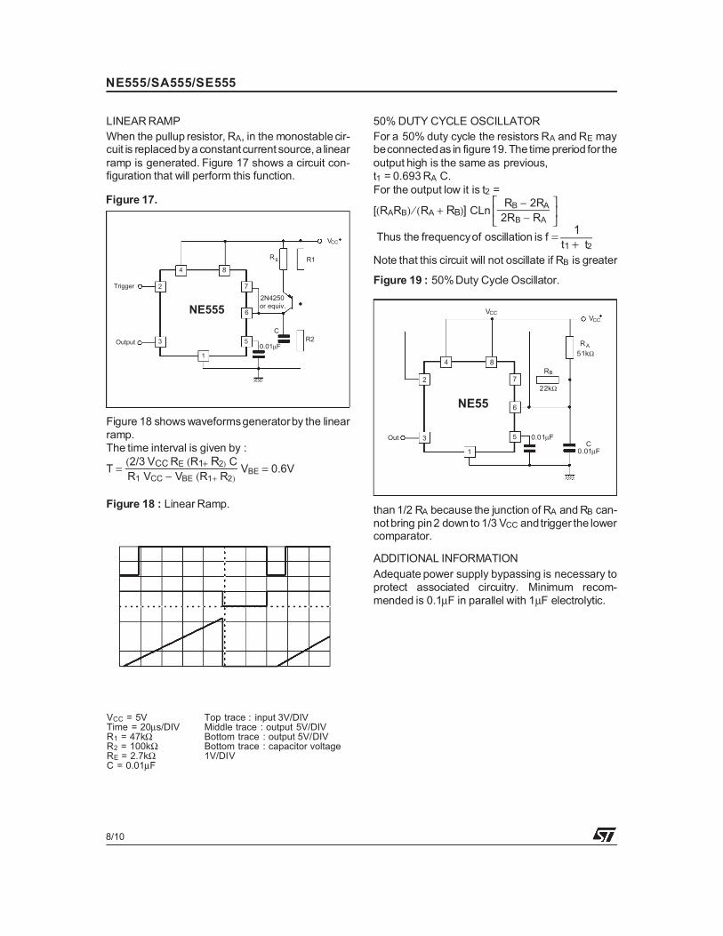
LINEARRAMP
When the pullup resistor, RA, in the monostable cir-cuit is replacedbya constantcurrent source,a linear
ramp is generated. Figure 17 shows a circuit con-figuration that will perform this function.
Trigger
Output
C
NE555
2
4
3
1
5
6
7
8
E
VCC
0.01µFR2
R1R
2N4250
or equiv.
Figure 17.
Out
RA
C
NE55
2
4
3
1
5
6
7
8
VCC
51kΩ
RB
22kΩ
0.01µF
VCC
0.01µF
Figure 19 : 50%Duty Cycle Oscillator.
Figure 18 showswaveformsgeneratorby the linear
ramp.
The time interval is given by :
T =(2/3 VCCRE (R1+ R2) C
R1 VCC − VBE (R1+ R2)VBE = 0.6V
Figure 18 : Linear Ramp.
VCC = 5V Top trace : input 3V/DIVTime = 20µs/DIV Middle trace : output 5V/DIVR1 = 47kΩ Bottom trace : output 5V/DIVR2 = 100kΩ Bottom trace : capacitor voltageRE = 2.7kΩ 1V/DIVC = 0.01µF
50%DUTY CYCLE OSCILLATOR
For a 50% duty cycle the resistors RA andRE maybeconnectedas in figure19.The time preriod for the
output high is the same as previous,
t1 = 0.693RA C.
For the output low it is t2 =
[(RARB) ⁄ (RA + RB)] CLn
RB − 2RA2RB − RA
Thus the frequencyof oscillation is f = 1
t1 + t2
Note that this circuit will not oscillate if RB is greater
than1/2 RA because the junction of RA andRB can-
notbring pin2 down to 1/3 VCC andtrigger the lowercomparator.
ADDITIONAL INFORMATION
Adequate power supply bypassing is necessary to
protect associated circuitry. Minimum recom-
mended is 0.1µF in parallel with 1µF electrolytic.
NE555/SA555/SE555
8/10

PM-DIP8.EPS
PACKAGE MECHANICAL DATA
8 PINS - PLASTIC DIP
DimensionsMillimeters Inches
Min. Typ. Max. Min. Typ. Max.
A 3.32 0.131
a1 0.51 0.020
B 1.15 1.65 0.045 0.065
b 0.356 0.55 0.014 0.022
b1 0.204 0.304 0.008 0.012
D 10.92 0.430
E 7.95 9.75 0.313 0.384
e 2.54 0.100
e3 7.62 0.300
e4 7.62 0.300
F 6.6 0260
i 5.08 0.200
L 3.18 3.81 0.125 0.150
Z 1.52 0.060
DIP8.TBL
NE555/SA555/SE555
9/10

PM-SO8.EPS
PACKAGE MECHANICAL DATA
8 PINS - PLASTIC MICROPACKAGE (SO)
DimensionsMillimeters Inches
Min. Typ. Max. Min. Typ. Max.
A 1.75 0.069
a1 0.1 0.25 0.004 0.010
a2 1.65 0.065
a3 0.65 0.85 0.026 0.033
b 0.35 0.48 0.014 0.019
b1 0.19 0.25 0.007 0.010
C 0.25 0.5 0.010 0.020
c1 45o(typ.)
D 4.8 5.0 0.189 0.197
E 5.8 6.2 0.228 0.244
e 1.27 0.050
e3 3.81 0.150
F 3.8 4.0 0.150 0.157
L 0.4 1.27 0.016 0.050
M 0.6 0.024
S 8o(max.)
SO8.TBL
Information furnished is believed to be accurate and reliable. However, STMicroelectronics assumes no responsibility for the
consequences of use of such information nor for any infringement of patents or other rights of third parties which may resultfrom its use. No license is granted by implication or otherwise under any patent or patent rights of STMicroelectronics. Specifi-
cations mentioned in this publication are subject to change without notice. This publication supersedes and replaces all infor-
mation previously supplied. STMicroelectronics products are not authorized for use as critical components in life supportdevices or systems without express written approval of STMicroelectronics.
The ST logo is a trademark of STMicroelectronics
1998 STMicroelectronics – Printed in Italy – All Rights Reserved
STMicroelectronics GROUP OF COMPANIES
Australia - Brazil - Canada - China - France - Germany - Italy - Japan - Korea - Malaysia - Malta - Mexico - MoroccoThe Netherlands - Singapore - Spain - Sweden - Switzerland - Taiwan - Thailand - United Kingdom- U.S.A. O
RDERCODE:
NE555/SA555/SE555
10/10

This datasheet has been download from:
www.datasheetcatalog.com
Datasheets for electronics components.

General DescriptionThe MAX220–MAX249 family of line drivers/receivers isintended for all EIA/TIA-232E and V.28/V.24 communica-tions interfaces, particularly applications where ±12V isnot available.
These parts are especially useful in battery-powered sys-tems, since their low-power shutdown mode reducespower dissipation to less than 5µW. The MAX225,MAX233, MAX235, and MAX245/MAX246/MAX247 useno external components and are recommended for appli-cations where printed circuit board space is critical.
________________________Applications
Portable Computers
Low-Power Modems
Interface Translation
Battery-Powered RS-232 Systems
Multidrop RS-232 Networks
____________________________Features
Superior to Bipolar Operate from Single +5V Power Supply
(+5V and +12V—MAX231/MAX239)
Low-Power Receive Mode in Shutdown(MAX223/MAX242)
Meet All EIA/TIA-232E and V.28 Specifications
Multiple Drivers and Receivers
3-State Driver and Receiver Outputs
Open-Line Detection (MAX243)
Ordering Information
Ordering Information continued at end of data sheet.
*Contact factory for dice specifications.
MA
X2
20
–M
AX
24
9
+5V-Powered, Multichannel RS-232Drivers/Receivers
________________________________________________________________ Maxim Integrated Products 1
Selection Table
19-4323; Rev 11; 2/03
PART
MAX220CPE
MAX220CSE
MAX220CWE 0°C to +70°C
0°C to +70°C
0°C to +70°C
TEMP RANGE PIN-PACKAGE
16 Plastic DIP
16 Narrow SO
16 Wide SO
MAX220C/D 0°C to +70°C Dice*
MAX220EPE
MAX220ESE
MAX220EWE -40°C to +85°C
-40°C to +85°C
-40°C to +85°C 16 Plastic DIP
16 Narrow SO
16 Wide SO
MAX220EJE -40°C to +85°C 16 CERDIP
MAX220MJE -55°C to +125°C 16 CERDIP
Power No. of Nominal SHDN RxPart Supply RS-232 No. of Cap. Value & Three- Active in Data RateNumber (V) Drivers/Rx Ext. Caps (µF) State SHDN (kbps) FeaturesMAX220 +5 2/2 4 0.1 No — 120 Ultra-low-power, industry-standard pinoutMAX222 +5 2/2 4 0.1 Yes — 200 Low-power shutdownMAX223 (MAX213) +5 4/5 4 1.0 (0.1) Yes 120 MAX241 and receivers active in shutdownMAX225 +5 5/5 0 — Yes 120 Available in SOMAX230 (MAX200) +5 5/0 4 1.0 (0.1) Yes — 120 5 drivers with shutdownMAX231 (MAX201) +5 and 2/2 2 1.0 (0.1) No — 120 Standard +5/+12V or battery supplies;
+7.5 to +13.2 same functions as MAX232MAX232 (MAX202) +5 2/2 4 1.0 (0.1) No — 120 (64) Industry standardMAX232A +5 2/2 4 0.1 No — 200 Higher slew rate, small capsMAX233 (MAX203) +5 2/2 0 — No — 120 No external capsMAX233A +5 2/2 0 — No — 200 No external caps, high slew rateMAX234 (MAX204) +5 4/0 4 1.0 (0.1) No — 120 Replaces 1488MAX235 (MAX205) +5 5/5 0 — Yes — 120 No external capsMAX236 (MAX206) +5 4/3 4 1.0 (0.1) Yes — 120 Shutdown, three stateMAX237 (MAX207) +5 5/3 4 1.0 (0.1) No — 120 Complements IBM PC serial portMAX238 (MAX208) +5 4/4 4 1.0 (0.1) No — 120 Replaces 1488 and 1489MAX239 (MAX209) +5 and 3/5 2 1.0 (0.1) No — 120 Standard +5/+12V or battery supplies;
+7.5 to +13.2 single-package solution for IBM PC serial portMAX240 +5 5/5 4 1.0 Yes — 120 DIP or flatpack packageMAX241 (MAX211) +5 4/5 4 1.0 (0.1) Yes — 120 Complete IBM PC serial portMAX242 +5 2/2 4 0.1 Yes 200 Separate shutdown and enableMAX243 +5 2/2 4 0.1 No — 200 Open-line detection simplifies cablingMAX244 +5 8/10 4 1.0 No — 120 High slew rateMAX245 +5 8/10 0 — Yes 120 High slew rate, int. caps, two shutdown modesMAX246 +5 8/10 0 — Yes 120 High slew rate, int. caps, three shutdown modesMAX247 +5 8/9 0 — Yes 120 High slew rate, int. caps, nine operating modesMAX248 +5 8/8 4 1.0 Yes 120 High slew rate, selective half-chip enablesMAX249 +5 6/10 4 1.0 Yes 120 Available in quad flatpack package
For pricing, delivery, and ordering information, please contact Maxim/Dallas Direct! at 1-888-629-4642, or visit Maxim’s website at www.maxim-ic.com.

MA
X2
20
–M
AX
24
9
+5V-Powered, Multichannel RS-232Drivers/Receivers
2 _______________________________________________________________________________________
ABSOLUTE MAXIMUM RATINGS—MAX220/222/232A/233A/242/243
ELECTRICAL CHARACTERISTICS—MAX220/222/232A/233A/242/243(VCC = +5V ±10%, C1–C4 = 0.1µF‚ MAX220, C1 = 0.047µF, C2–C4 = 0.33µF, TA = TMIN to TMAX‚ unless otherwise noted.)
Note 1: Input voltage measured with TOUT in high-impedance state, SHDN or VCC = 0V.
Note 2: For the MAX220, V+ and V- can have a maximum magnitude of 7V, but their absolute difference cannot exceed 13V.
Stresses beyond those listed under “Absolute Maximum Ratings” may cause permanent damage to the device. These are stress ratings only, and functionaloperation of the device at these or any other conditions beyond those indicated in the operational sections of the specifications is not implied. Exposure toabsolute maximum rating conditions for extended periods may affect device reliability.
Supply Voltage (VCC) ...............................................-0.3V to +6VInput VoltagesTIN..............................................................-0.3V to (VCC - 0.3V)RIN (Except MAX220) ........................................................±30VRIN (MAX220).....................................................................±25VTOUT (Except MAX220) (Note 1) .......................................±15VTOUT (MAX220)...............................................................±13.2V
Output VoltagesTOUT...................................................................................±15VROUT.........................................................-0.3V to (VCC + 0.3V)
Driver/Receiver Output Short Circuited to GND.........ContinuousContinuous Power Dissipation (TA = +70°C)16-Pin Plastic DIP (derate 10.53mW/°C above +70°C)....842mW18-Pin Plastic DIP (derate 11.11mW/°C above +70°C)....889mW
20-Pin Plastic DIP (derate 8.00mW/°C above +70°C) ..440mW16-Pin Narrow SO (derate 8.70mW/°C above +70°C) ...696mW16-Pin Wide SO (derate 9.52mW/°C above +70°C)......762mW18-Pin Wide SO (derate 9.52mW/°C above +70°C)......762mW20-Pin Wide SO (derate 10.00mW/°C above +70°C)....800mW20-Pin SSOP (derate 8.00mW/°C above +70°C) ..........640mW16-Pin CERDIP (derate 10.00mW/°C above +70°C).....800mW18-Pin CERDIP (derate 10.53mW/°C above +70°C).....842mW
Operating Temperature RangesMAX2_ _AC_ _, MAX2_ _C_ _.............................0°C to +70°CMAX2_ _AE_ _, MAX2_ _E_ _ ..........................-40°C to +85°CMAX2_ _AM_ _, MAX2_ _M_ _.......................-55°C to +125°C
Storage Temperature Range .............................-65°C to +160°CLead Temperature (soldering, 10s) .................................+300°C
V1.4 0.8Input Logic Threshold Low
UNITSMIN TYP MAXPARAMETER CONDITIONS
Input Logic Threshold HighAll devices except MAX220 2 1.4
V
All except MAX220, normal operation 5 40Logic Pull-Up/lnput Current
SHDN = 0V, MAX222/242, shutdown, MAX220 ±0.01 ±1µA
VCC = 5.5V, SHDN = 0V, VOUT = ±15V, MAX222/242 ±0.01 ±10Output Leakage Current
VCC = SHDN = 0V, VOUT = ±15V ±0.01 ±10µA
200 116Data Rate kbps
Transmitter Output Resistance VCC = V+ = V- = 0V, VOUT = ±2V 300 10M Ω
Output Short-Circuit Current VOUT = 0V ±7 ±22 mA
RS-232 Input Voltage Operating Range ±30 V
All except MAX243 R2IN 0.8 1.3RS-232 Input Threshold Low VCC = 5V
MAX243 R2IN (Note 2) -3V
All except MAX243 R2IN 1.8 2.4RS-232 Input Threshold High VCC = 5V
MAX243 R2IN (Note 2) -0.5 -0.1V
All except MAX243, VCC = 5V, no hysteresis in shdn. 0.2 0.5 1RS-232 Input Hysteresis
MAX243 1V
RS-232 Input Resistance 3 5 7 kΩ
TTL/CMOS Output Voltage Low IOUT = 3.2mA 0.2 0.4 V
TTL/CMOS Output Voltage High IOUT = -1.0mA 3.5 VCC - 0.2 V
Sourcing VOUT = GND -2 -10mATTL/CMOS Output Short-Circuit Current
Shrinking VOUT = VCC 10 30
V±5 ±8Output Voltage Swing All transmitter outputs loaded with 3kΩ to GND
RS-232 TRANSMITTERS
RS-232 RECEIVERS
2.4MAX220: VCC = 5.0V

MA
X2
20
–M
AX
24
9
+5V-Powered, Multichannel RS-232Drivers/Receivers
_______________________________________________________________________________________ 3
Note 3: MAX243 R2OUT is guaranteed to be low when R2IN is ≥ 0V or is floating.
ELECTRICAL CHARACTERISTICS—MAX220/222/232A/233A/242/243 (continued)(VCC = +5V ±10%, C1–C4 = 0.1µF‚ MAX220, C1 = 0.047µF, C2–C4 = 0.33µF, TA = TMIN to TMAX‚ unless otherwise noted.)
Operating Supply Voltage
SHDN Threshold High
4.5 5.5 V
MAX222/242
Transmitter-Output Enable Time
(SHDN Goes High), Figure 4
2.0 1.4 V
MAX220 0.5 2
tET
No loadMAX222/232A/233A/242/243 4 10
MAX222/232A/233A/242/243 6 12 30
MAX220 12
VCC Supply Current (SHDN = VCC),
Figures 5, 6, 11, 19 3kΩ load
both inputs MAX222/232A/233A/242/243 15
mA
Transition Slew Rate
TA = +25°C 0.1 10
CL = 50pF to 2500pF,
RL = 3kΩ to 7kΩ,
VCC = 5V, TA = +25°C,
measured from +3V
to -3V or -3V to +3V
TA = 0°C to +70°C
CONDITIONS
2 50
MAX220 1.5 3 30
V/µs
TA = -40°C to +85°C 2 50
MAX222/242, 0.1µF caps(includes charge-pump start-up)
Shutdown Supply Current MAX222/242
TA = -55°C to +125°C 35 100
µA
SHDN Input Leakage Current MAX222/242 ±1 µA
SHDN Threshold Low MAX222/242 1.4 0.8 V
250
MAX222/232A/233A/242/243 1.3 3.5
µs
tPHLTMAX220 4 10
Transmitter-Output Disable Time
(SHDN Goes Low), Figure 4tDT
MAX222/232A/233A/242/243 1.5 3.5
Transmitter Propagation Delay
TLL to RS-232 (Normal Operation),
Figure 1 tPLHTMAX220 5 10
µs
V2.0 1.4
MAX222/242, 0.1µF caps
µA±0.05 ±10
600
TTL/CMOS Output Leakage Current
EN Input Threshold High
MAX222/232A/233A/242/243 0.5 1
ns
tPHLRMAX220 0.6 3
tPLHRMAX222/232A/233A/242/243 0.6 1
Receiver Propagation Delay
RS-232 to TLL (Normal Operation),
Figure 2
tPHLT - tPLHT
MAX220 0.8 3
µs
MAX222/232A/233A/242/243
tPHLS MAX242 0.5 10Receiver Propagation Delay
RS-232 to TLL (Shutdown), Figure 2 tPLHS MAX242 2.5 10µs
Receiver-Output Enable Time, Figure 3 tER MAX242
UNITSMIN TYP MAX
125 500
PARAMETER
MAX242
ns
SHDN = VCC or EN = VCC (SHDN = 0V for MAX222),
0V ≤ VOUT ≤ VCC
Receiver-Output Disable Time, Figure 3 tDR MAX242 160 500 ns
300ns
Transmitter + to - Propagation
Delay Difference (Normal Operation) MAX220 2000
tPHLR - tPLHRMAX222/232A/233A/242/243 100
nsReceiver + to - Propagation
Delay Difference (Normal Operation) MAX220 225
V1.4 0.8EN Input Threshold Low MAX242

MA
X2
20
–M
AX
24
9
+5V-Powered, Multichannel RS-232Drivers/Receivers
4 _______________________________________________________________________________________
__________________________________________Typical Operating Characteristics
MAX220/MAX222/MAX232A/MAX233A/MAX242/MAX243
10
8
-100 5 15 25
OUTPUT VOLTAGE vs. LOAD CURRENT
-4
-6
-8
-2
6
4
2
MA
X2
20
-01
LOAD CURRENT (mA)
OU
TPU
T V
OLT
AG
E (V
)
10
0
20
0.1µF
EITHER V+ OR V- LOADED
VCC = ±5VNO LOAD ONTRANSMITTER OUTPUTS(EXCEPT MAX220, MAX233A)
V- LOADED, NO LOAD ON V+
V+ LOADED, NO LOAD ON V-
1µF
1µF0.1µF
11
10
40 10 40 60
AVAILABLE OUTPUT CURRENT
vs. DATA RATE
6
5
7
9
8
MA
X2
20
-02
DATA RATE (kbits/sec)
OU
TPU
T C
UR
REN
T (m
A)
20 30 50
OUTPUT LOAD CURRENTFLOWS FROM V+ TO V-
VCC = +5.25V
ALL CAPS1µF
ALL CAPS0.1µF
VCC = +4.75V
+10V
-10V
MAX222/MAX242
ON-TIME EXITING SHUTDOWN
+5V+5V
0V
0V
MA
X2
20
-03
500µs/div
V+,
V-
VO
LTA
GE
(V)
1µF CAPSV+
V+
V-V-
SHDN
0.1µF CAPS
1µF CAPS
0.1µF CAPS

MA
X2
20
–M
AX
24
9
+5V-Powered, Multichannel RS-232Drivers/Receivers
_______________________________________________________________________________________ 5
VCC ...........................................................................-0.3V to +6VV+................................................................(VCC - 0.3V) to +14VV- ............................................................................+0.3V to -14VInput VoltagesTIN ............................................................-0.3V to (VCC + 0.3V)RIN......................................................................................±30V
Output VoltagesTOUT ...................................................(V+ + 0.3V) to (V- - 0.3V)ROUT .........................................................-0.3V to (VCC + 0.3V)
Short-Circuit Duration, TOUT ......................................ContinuousContinuous Power Dissipation (TA = +70°C)14-Pin Plastic DIP (derate 10.00mW/°C above +70°C)....800mW16-Pin Plastic DIP (derate 10.53mW/°C above +70°C)....842mW20-Pin Plastic DIP (derate 11.11mW/°C above +70°C)....889mW24-Pin Narrow Plastic DIP
(derate 13.33mW/°C above +70°C) ..........1.07W24-Pin Plastic DIP (derate 9.09mW/°C above +70°C)......500mW16-Pin Wide SO (derate 9.52mW/°C above +70°C).........762mW
20-Pin Wide SO (derate 10 00mW/°C above +70°C).......800mW24-Pin Wide SO (derate 11.76mW/°C above +70°C).......941mW28-Pin Wide SO (derate 12.50mW/°C above +70°C) .............1W44-Pin Plastic FP (derate 11.11mW/°C above +70°C) .....889mW14-Pin CERDIP (derate 9.09mW/°C above +70°C) ..........727mW16-Pin CERDIP (derate 10.00mW/°C above +70°C) ........800mW20-Pin CERDIP (derate 11.11mW/°C above +70°C) ........889mW24-Pin Narrow CERDIP
(derate 12.50mW/°C above +70°C) ..............1W24-Pin Sidebraze (derate 20.0mW/°C above +70°C)..........1.6W28-Pin SSOP (derate 9.52mW/°C above +70°C).............762mW
Operating Temperature RangesMAX2 _ _ C _ _......................................................0°C to +70°CMAX2 _ _ E _ _ ...................................................-40°C to +85°CMAX2 _ _ M _ _ ...............................................-55°C to +125°C
Storage Temperature Range .............................-65°C to +160°CLead Temperature (soldering, 10s) .................................+300°C
ABSOLUTE MAXIMUM RATINGS—MAX223/MAX230–MAX241
ELECTRICAL CHARACTERISTICS—MAX223/MAX230–MAX241(MAX223/230/232/234/236/237/238/240/241, VCC = +5V ±10; MAX233/MAX235, VCC = 5V ±5%‚ C1–C4 = 1.0µF; MAX231/MAX239,
VCC = 5V ±10%; V+ = 7.5V to 13.2V; TA = TMIN to TMAX; unless otherwise noted.)
Stresses beyond those listed under “Absolute Maximum Ratings” may cause permanent damage to the device. These are stress ratings only, and functional
operation of the device at these or any other conditions beyond those indicated in the operational sections of the specifications is not implied. Exposure to
absolute maximum rating conditions for extended periods may affect device reliability.
CONDITIONS MIN TYP MAX UNITS
Output Voltage Swing All transmitter outputs loaded with 3kΩ to ground ±5.0 ±7.3 V
VCC Power-Supply CurrentNo load,
TA = +25°C
5 10
mA7 15
0.4 1
V+ Power-Supply Current1.8 5
mA5 15
Shutdown Supply Current TA = +25°C15 50
VInput Logic Threshold High
TIN 2.0
EN, SHDN (MAX223);
EN, SHDN (MAX230/235/236/240/241)2.4
Logic Pull-Up Current TIN = 0V 1.5 200
Receiver Input Voltage
Operating Range-30 30 V
µA
µA1 10
VInput Logic Threshold Low TIN; EN, SHDN (MAX233); EN, SHDN (MAX230/235–241) 0.8
MAX231/239
MAX223/230/234–238/240/241
MAX232/233
PARAMETER
MAX239
MAX230/235/236/240/241
MAX231
MAX223

mA
MA
X2
20
–M
AX
24
9
+5V-Powered, Multichannel RS-232Drivers/Receivers
6 _______________________________________________________________________________________
V
0.8 1.2
PARAMETER MIN TYP MAX UNITSCONDITIONS
Normal operation
SHDN = 5V (MAX223)
SHDN = 0V (MAX235/236/240/241)
1.7 2.4
RS-232 Input Threshold LowTA = +25°C,
VCC = 5V
0.6 1.5
VRS-232 Input Threshold HighTA = +25°C,
VCC = 5V Shutdown (MAX223)
SHDN = 0V,
EN = 5V (R4IN‚ R5IN)
1.5 2.4
ELECTRICAL CHARACTERISTICS—MAX223/MAX230–MAX241 (continued)(MAX223/230/232/234/236/237/238/240/241, VCC = +5V ±10; MAX233/MAX235, VCC = 5V ±5%‚ C1–C4 = 1.0µF; MAX231/MAX239,
VCC = 5V ±10%; V+ = 7.5V to 13.2V; TA = TMIN to TMAX; unless otherwise noted.)
Shutdown (MAX223)
SHDN = 0V,
EN = 5V (R4IN, R5IN)
Normal operation
SHDN = 5V (MAX223)
SHDN = 0V (MAX235/236/240/241)
RS-232 Input Hysteresis VCC = 5V, no hysteresis in shutdown 0.2 0.5 1.0 V
RS-232 Input Resistance TA = +25°C, VCC = 5V 3 5 7 kΩ
TTL/CMOS Output Voltage Low IOUT = 1.6mA (MAX231/232/233, IOUT = 3.2mA) 0.4 V
TTL/CMOS Output Voltage High IOUT = -1mA 3.5 VCC - 0.4 V
TTL/CMOS Output Leakage Current0V ≤ ROUT ≤ VCC; EN = 0V (MAX223);
EN = VCC (MAX235–241 )0.05 ±10 µA
MAX223 600nsReceiver Output Enable Time
Normal
operation MAX235/236/239/240/241 400
MAX223 900nsReceiver Output Disable Time
Normal
operation MAX235/236/239/240/241 250
Normal operation 0.5 10
µsSHDN = 0V
(MAX223)
4 40Propagation Delay
RS-232 IN to
TTL/CMOS OUT,
CL = 150pF6 40
3 5.1 30
V/µsMAX231/MAX232/MAX233, TA = +25°C, VCC = 5V,
RL = 3kΩ to 7kΩ, CL = 50pF to 2500pF, measured from
+3V to -3V or -3V to +3V
4 30
Transmitter Output Resistance VCC = V+ = V- = 0V, VOUT = ±2V 300 Ω
Transmitter Output Short-Circuit
Current±10 mA
tPHLS
tPLHS
Transition Region Slew Rate
MAX223/MAX230/MAX234–241, TA = +25°C, VCC = 5V,
RL = 3kΩ to 7kΩ‚ CL = 50pF to 2500pF, measured from
+3V to -3V or -3V to +3V

MA
X2
20
–M
AX
24
9
+5V-Powered, Multichannel RS-232Drivers/Receivers
_______________________________________________________________________________________ 7
8.5
6.54.5 5.5
TRANSMITTER OUTPUT
VOLTAGE (VOH) vs. VCC
7.0
8.0
MA
X2
20
-04
VCC (V)
VO
H (
V)
5.0
7.5
1 TRANSMITTERLOADED
3 TRANS-MITTERSLOADED
4 TRANSMITTERSLOADED
2 TRANSMITTERSLOADED
TA = +25°CC1–C4 = 1µFTRANSMITTERLOADS =3kΩ || 2500pF
7.4
6.00 2500
TRANSMITTER OUTPUT VOLTAGE (VOH)
vs. LOAD CAPACITANCE AT
DIFFERENT DATA RATES
6.4
6.2
7.2
7.0
MA
X2
20
-05
LOAD CAPACITANCE (pF)
VO
H (
V)
15001000500 2000
6.8
6.6
160kbits/sec80kbits/sec20kbits/sec
TA = +25°CVCC = +5V3 TRANSMITTERS LOADEDRL = 3kΩ
C1–C4 = 1µF
12.0
4.00 2500
TRANSMITTER SLEW RATE
vs. LOAD CAPACITANCE
6.0
5.0
11.0
9.0
10.0
MA
X2
20
-06
LOAD CAPACITANCE (pF)
SLE
W R
ATE
(V
/µs)
15001000500 2000
8.0
7.0
TA = +25°CVCC = +5VLOADED, RL = 3kΩ
C1–C4 = 1µF
1 TRANSMITTER LOADED
2 TRANSMITTERS LOADED
3 TRANSMITTERS LOADED
4 TRANSMITTERS LOADED
-6.0
-9.04.5 5.5
TRANSMITTER OUTPUT
VOLTAGE (VOL) vs. VCC
-8.0
-8.5
-6.5
-7.0
MA
X2
20
-07
VCC (V)
VO
L (V
)
5.0
-7.5
4 TRANS-MITTERSLOADED
TA = +25°CC1–C4 = 1µFTRANSMITTERLOADS =3kΩ || 2500pF
1 TRANS-MITTERLOADED
2 TRANS-MITTERSLOADED
3 TRANS-MITTERSLOADED
-6.0
-7.60 2500
TRANSMITTER OUTPUT VOLTAGE (VOL)
vs. LOAD CAPACITANCE AT
DIFFERENT DATA RATES
-7.0
-7.2
-7.4
-6.2
-6.4
MA
X2
20
-08
LOAD CAPACITANCE (pF)
VO
L (V
)
15001000500 2000
-6.6
-6.8160kbits/sec80kbits/sec20Kkbits/sec
TA = +25°CVCC = +5V3 TRANSMITTERS LOADEDRL = 3kΩ
C1–C4 = 1µF
10
-100 5 10 15 20 25 30 35 40 45 50
TRANSMITTER OUTPUT VOLTAGE (V+, V-)
vs. LOAD CURRENT
-2
-6
-4
-8
8
6
MA
X2
20
-09
CURRENT (mA)
V+,
V-
(V)
4
2
0V+ AND V-EQUALLYLOADED
V- LOADED,NO LOADON V+
TA = +25°CVCC = +5VC1–C4 = 1µF
ALL TRANSMITTERS UNLOADED
V+ LOADED,NO LOADON V-
__________________________________________Typical Operating Characteristics
MAX223/MAX230–MAX241
*SHUTDOWN POLARITY IS REVERSED FOR NON MAX241 PARTS
V+, V- WHEN EXITING SHUTDOWN
(1µF CAPACITORS)MAX220-13
SHDN*
V-
O
V+
500ms/div

Input Logic Threshold Low
MA
X2
20
–M
AX
24
9
+5V-Powered, Multichannel RS-232Drivers/Receivers
8 _______________________________________________________________________________________
ABSOLUTE MAXIMUM RATINGS—MAX225/MAX244–MAX249
ELECTRICAL CHARACTERISTICS—MAX225/MAX244–MAX249(MAX225, VCC = 5.0V ±5%; MAX244–MAX249, VCC = +5.0V ±10%, external capacitors C1–C4 = 1µF; TA = TMIN to TMAX; unless oth-erwise noted.)
Note 4: Input voltage measured with transmitter output in a high-impedance state, shutdown, or VCC = 0V.
Stresses beyond those listed under “Absolute Maximum Ratings” may cause permanent damage to the device. These are stress ratings only, and functional
operation of the device at these or any other conditions beyond those indicated in the operational sections of the specifications is not implied. Exposure to
absolute maximum rating conditions for extended periods may affect device reliability.
Supply Voltage (VCC) ...............................................-0.3V to +6VInput VoltagesTIN‚ ENA, ENB, ENR, ENT, ENRA,ENRB, ENTA, ENTB..................................-0.3V to (VCC + 0.3V)RIN .....................................................................................±25VTOUT (Note 3).....................................................................±15VROUT ........................................................-0.3V to (VCC + 0.3V)
Short Circuit (one output at a time)TOUT to GND............................................................ContinuousROUT to GND............................................................Continuous
Continuous Power Dissipation (TA = +70°C)28-Pin Wide SO (derate 12.50mW/°C above +70°C) .............1W40-Pin Plastic DIP (derate 11.11mW/°C above +70°C) ...611mW44-Pin PLCC (derate 13.33mW/°C above +70°C) ...........1.07W
Operating Temperature RangesMAX225C_ _, MAX24_C_ _ ..................................0°C to +70°CMAX225E_ _, MAX24_E_ _ ...............................-40°C to +85°C
Storage Temperature Range .............................-65°C to +160°CLead Temperature (soldering,10s) ..................................+300°C
VCC = 0V,
VOUT = ±15V
µATables 1a–1d
±0.01 ±25
Normal operation
Shutdown
Tables 1a–1d, normal operation
All transmitter outputs loaded with 3kΩ to GND
ENA, ENB, ENT, ENTA, ENTB =
VCC, VOUT = ±15V
VRS-232 Input Hysteresis
RS-232 Input Threshold Low V
V±5 ±7.5Output Voltage Swing
Output Leakage Current (Shutdown)
±0.01 ±25
Ω300 10MVCC = V+ = V- = 0V, VOUT = ±2V (Note 4)Transmitter Output Resistance
µA
PARAMETER
±0.05 ±0.10
MIN TYP MAX UNITS
Normal operation, outputs disabled,
Tables 1a–1d, 0V ≤ VOUT ≤ VCC, ENR_ = VCCTTL/CMOS Output Leakage Current
10 30Shrinking VOUT = VCCmA
-2 -10Sourcing VOUT = GND
V3.5 VCC - 0.2IOUT = -1.0mATTL/CMOS Output Voltage High
V0.2 0.4IOUT = 3.2mATTL/CMOS Output Voltage Low
kΩ3 5 7
0.2 0.5 1.0VCC = 5V
1.4 0.8 V
TTL/CMOS Output Short-Circuit Current
V1.8 2.4
0.8 1.3VCC = 5V
RS-232 Input Resistance
V±25RS-232 Input Voltage Operating Range
mA±7 ±30VOUT = 0VOutput Short-Circuit Current
kbps120 64Data Rate
CONDITIONS
VCC = 5V
µA±0.01 ±1
Logic Pull-Up/lnput Current10 50
Tables 1a–1d
RS-232 Input Threshold High
V2 1.4Input Logic Threshold High
RS-232 TRANSMITTERS
RS-232 RECEIVERS

MA
X2
20
–M
AX
24
9
+5V-Powered, Multichannel RS-232Drivers/Receivers
_______________________________________________________________________________________ 9
Operating Supply Voltage4.75 5.25
V
Transmitter Enable Time
MAX225 10 20
tET
No loadMAX244–MAX249 11 30
5 10 30
MAX225 40
VCC Supply Current
(Normal Operation) 3kΩ loads on
all outputs MAX244–MAX249 57
mA
Transition Slew Rate
8 25
CL = 50pF to 2500pF, RL = 3kΩ to 7kΩ, VCC = 5V,
TA = +25°C, measured from +3V to -3V or -3V to +3V
TA = TMIN to TMAX
CONDITIONS
50
V/µs
MAX246–MAX249 (excludes charge-pump startup)
Shutdown Supply Current µA
5
tPHLT 1.3 3.5
µs
tPLHT 1.5 3.5
Transmitter Disable Time, Figure 4
Transmitter Propagation Delay
TLL to RS-232 (Normal Operation),
Figure 1
µs
tDT 100 ns
Transmitter + to - Propagation
Delay Difference (Normal Operation)tPHLT - tPLHT
UNITSMIN TYP MAX
350
PARAMETER
ns
Receiver + to - Propagation
Delay Difference (Normal Operation)tPHLR - tPLHR 350 ns
4.5 5.5MAX244–MAX249
MAX225
Leakage current ±1
Threshold low 1.4 0.8Control Input
Threshold high 2.4 1.4V
µA
TA = +25°C
tPHLR 0.6 1.5
tPLHR 0.6 1.5
Receiver Propagation Delay
TLL to RS-232 (Normal Operation),
Figure 2
µs
tPHLS 0.6 10
tPLHS 3.0 10
Receiver Propagation Delay
TLL to RS-232 (Low-Power Mode),
Figure 2
µs
Receiver-Output Enable Time, Figure 3 tER 100 500 ns
Receiver-Output Disable Time, Figure 3 tDR 100 500 ns
MAX225/MAX245–MAX249(includes charge-pump startup)
10 ms
POWER SUPPLY AND CONTROL LOGIC
AC CHARACTERISTICS
Note 5: The 300Ω minimum specification complies with EIA/TIA-232E, but the actual resistance when in shutdown mode or VCC =
0V is 10MΩ as is implied by the leakage specification.
ELECTRICAL CHARACTERISTICS—MAX225/MAX244–MAX249 (continued)(MAX225, VCC = 5.0V ±5%; MAX244–MAX249, VCC = +5.0V ±10%, external capacitors C1–C4 = 1µF; TA = TMIN to TMAX; unless oth-erwise noted.)

MA
X2
20
–M
AX
24
9
+5V-Powered, Multichannel RS-232Drivers/Receivers
10 ______________________________________________________________________________________
__________________________________________Typical Operating Characteristics
MAX225/MAX244–MAX249
18
20 1 2 3 4 5
TRANSMITTER SLEW RATE
vs. LOAD CAPACITANCE
8
6
4
16 MA
X2
20
-10
LOAD CAPACITANCE (nF)
TRA
NS
MIT
TER
SLE
W R
ATE
(V
/µs)
14
12
10
VCC = 5V
EXTERNAL POWER SUPPLY1µF CAPACITORS
40kb/s DATA RATE 8 TRANSMITTERSLOADED WITH 3kΩ
10
-100 5 10 15 20 25 30 35
OUTPUT VOLTAGE
vs. LOAD CURRENT FOR V+ AND V-
-2
-4
-6
-8
8
MA
X2
20
-11
LOAD CURRENT (mA)
OU
TPU
T V
OLT
AG
E (V
)
6
4
2
0
V+ AND V- LOADED
EITHER V+ OR V- LOADED
V+ AND V- LOADED
VCC = 5VEXTERNAL CHARGE PUMP1µF CAPACITORS 8 TRANSMITTERSDRIVING 5kΩ AND2000pF AT 20kbits/sec
V- LOADED
V+ LOADED
9.0
5.00 1 2 3 4 5
TRANSMITTER OUTPUT VOLTAGE (V+, V-)
vs. LOAD CAPACITANCE AT
DIFFERENT DATA RATES
6.0
5.5
8.5 MA
X2
20
-12
LOAD CAPACITANCE (nF)
V+,
V (
V)
8.0
7.5
7.0
6.5
VCC = 5V WITH ALL TRANSMITTERS DRIVENLOADED WITH 5kΩ
10kb/sec
20kb/sec
40kb/sec
60kb/sec
100kb/sec
200kb/sec
ALL CAPACITIORS 1µF

MA
X2
20
–M
AX
24
9
+5V-Powered, Multichannel RS-232Drivers/Receivers
______________________________________________________________________________________ 11
INPUT
OUTPUT
+3V
V+
0V
V-
0V
tPLHT tPHLT
tPHLR
tPHLS
tPLHR
tPLHS
50%VCC
50%
+3V
50%INPUT
OUTPUT
*EXCEPT FOR R2 ON THE MAX243 WHERE -3V IS USED.
0V*
50%
GND
Figure 1. Transmitter Propagation-Delay Timing Figure 2. Receiver Propagation-Delay Timing
EN
RX IN
a) TEST CIRCUIT
b) ENABLE TIMING
c) DISABLE TIMING
EN INPUT
RECEIVEROUTPUTS
RX OUTRX
1kΩ
0V
+3V
EN
EN
+0.8V
+3.5V
OUTPUT ENABLE TIME (tER)
VCC - 2V
VOL + 0.5V
VOH - 0.5V
OUTPUT DISABLE TIME (tDR)
VCC - 2V
+3V
0V
150pF
EN INPUT
VOH
RECEIVEROUTPUTS
VOL
1 OR 0 TX
3kΩ 50pF
-5V
+5V
OUTPUT DISABLE TIME (tDT)
V+
SHDN+3V
0V
V-
0V
a) TIMING DIAGRAM
b) TEST CIRCUIT
Figure 3. Receiver-Output Enable and Disable Timing Figure 4. Transmitter-Output Disable Timing

MA
X2
20
–M
AX
24
9
+5V-Powered, Multichannel RS-232Drivers/Receivers
12 ______________________________________________________________________________________
ENT ENR OPERATION STATUS TRANSMITTERS RECEIVERS
0 0 Normal Operation All Active All Active
0 1 Normal Operation All Active All 3-State
1 0 Shutdown All 3-State All Low-Power Receive Mode
1 1 Shutdown All 3-State All 3-State
Table 1a. MAX245 Control Pin Configurations
ENT ENROPERATION
STATUS
TRANSMITTERS RECEIVERS
TA1–TA4 TB1–TB4 RA1–RA5 RB1–RB5
0 0 Normal Operation All Active All Active All Active All Active
0 1 Normal Operation All Active All ActiveRA1–RA4 3-State,
RA5 Active
RB1–RB4 3-State,
RB5 Active
1 0 Shutdown All 3-State All 3-StateAll Low-Power
Receive Mode
All Low-Power
Receive Mode
1 1 Shutdown All 3-State All 3-State
RA1–RA4 3-State,
RA5 Low-Power
Receive Mode
RB1–RB4 3-State,
RB5 Low-Power
Receive Mode
Table 1b. MAX245 Control Pin Configurations
Table 1c. MAX246 Control Pin Configurations
ENA ENBOPERATION
STATUS
TRANSMITTERS RECEIVERS
TA1–TA4 TB1–TB4 RA1–RA5 RB1–RB5
0 0 Normal Operation All Active All Active All Active All Active
0 1 Normal Operation All Active All 3-State All ActiveRB1–RB4 3-State,
RB5 Active
1 0 Shutdown All 3-State All ActiveRA1–RA4 3-State,
RA5 ActiveAll Active
1 1 Shutdown All 3-State All 3-State
RA1–RA4 3-State,
RA5 Low-Power
Receive Mode
RB1–RB4 3-State,
RA5 Low-Power
Receive Mode

MA
X2
20
–M
AX
24
9
+5V-Powered, Multichannel RS-232Drivers/Receivers
______________________________________________________________________________________ 13
TA1–TA4 TB1–TB4 RA1–RA4 RB1–RB4
0 0 0 0 Normal Operation All Active All Active All Active All Active
0 0 0 1 Normal Operation All Active All Active All Active
All 3-State, except
RB5 stays active on
MAX247
0 0 1 0 Normal Operation All Active All Active All 3-State All Active
0 0 1 1 Normal Operation All Active All Active All 3-State
All 3-State, except
RB5 stays active on
MAX247
0 1 0 0 Normal Operation All Active All 3-State All Active All Active
0 1 0 1 Normal Operation All Active All 3-State All Active
All 3-State, except
RB5 stays active on
MAX247
0 1 1 0 Normal Operation All Active All 3-State All 3-State All Active
0 1 1 1 Normal Operation All Active All 3-State All 3-State
All 3-State, except
RB5 stays active on
MAX247
1 0 0 0 Normal Operation All 3-State All Active All Active All Active
1 0 0 1 Normal Operation All 3-State All Active All Active
All 3-State, except
RB5 stays active on
MAX247
1 0 1 0 Normal Operation All 3-State All Active All 3-State All Active
1 0 1 1 Normal Operation All 3-State All Active All 3-State
All 3-State, except
RB5 stays active on
MAX247
1 1 0 0 Shutdown All 3-State All 3-StateLow-Power
Receive Mode
Low-Power
Receive Mode
1 1 0 1 Shutdown All 3-State All 3-StateLow-Power
Receive Mode
All 3-State, except
RB5 stays active on
MAX247
1 1 1 0 Shutdown All 3-State All 3-State All 3-StateLow-Power
Receive Mode
1 1 1 1 Shutdown All 3-State All 3-State All 3-State
All 3-State, except
RB5 stays active on
MAX247
Table 1d. MAX247/MAX248/MAX249 Control Pin Configurations
MAX248
OPERATION
STATUSENRB
MAX247 TA1–TA4 TB1–TB4 RA1–RA4 RB1–RB5
TRANSMITTERS
ENRAENTBENTA
MAX249 TA1–TA3 TB1–TB3 RA1–RA5 RB1–RB5
RECEIVERS

MA
X2
20
–M
AX
24
9 _______________Detailed DescriptionThe MAX220–MAX249 contain four sections: dualcharge-pump DC-DC voltage converters, RS-232 dri-vers, RS-232 receivers, and receiver and transmitterenable control inputs.
Dual Charge-Pump Voltage ConverterThe MAX220–MAX249 have two internal charge-pumpsthat convert +5V to ±10V (unloaded) for RS-232 driveroperation. The first converter uses capacitor C1 to dou-ble the +5V input to +10V on C3 at the V+ output. Thesecond converter uses capacitor C2 to invert +10V to -10V on C4 at the V- output.
A small amount of power may be drawn from the +10V(V+) and -10V (V-) outputs to power external circuitry(see the Typical Operating Characteristics section),except on the MAX225 and MAX245–MAX247, wherethese pins are not available. V+ and V- are not regulated,so the output voltage drops with increasing load current.Do not load V+ and V- to a point that violates the mini-mum ±5V EIA/TIA-232E driver output voltage whensourcing current from V+ and V- to external circuitry.
When using the shutdown feature in the MAX222,MAX225, MAX230, MAX235, MAX236, MAX240,MAX241, and MAX245–MAX249, avoid using V+ and V-to power external circuitry. When these parts are shutdown, V- falls to 0V, and V+ falls to +5V. For applica-tions where a +10V external supply is applied to the V+pin (instead of using the internal charge pump to gen-erate +10V), the C1 capacitor must not be installed andthe SHDN pin must be tied to VCC. This is because V+is internally connected to VCC in shutdown mode.
RS-232 DriversThe typical driver output voltage swing is ±8V whenloaded with a nominal 5kΩ RS-232 receiver and VCC =+5V. Output swing is guaranteed to meet the EIA/TIA-232E and V.28 specification, which calls for ±5V mini-mum driver output levels under worst-case conditions.These include a minimum 3kΩ load, VCC = +4.5V, andmaximum operating temperature. Unloaded driver out-put voltage ranges from (V+ -1.3V) to (V- +0.5V).
Input thresholds are both TTL and CMOS compatible.The inputs of unused drivers can be left unconnectedsince 400kΩ input pull-up resistors to VCC are built in(except for the MAX220). The pull-up resistors force theoutputs of unused drivers low because all drivers invert.The internal input pull-up resistors typically source 12µA,except in shutdown mode where the pull-ups are dis-abled. Driver outputs turn off and enter a high-imped-ance state—where leakage current is typicallymicroamperes (maximum 25µA)—when in shutdown
mode, in three-state mode, or when device power isremoved. Outputs can be driven to ±15V. The power-supply current typically drops to 8µA in shutdown mode.The MAX220 does not have pull-up resistors to force theoutputs of the unused drivers low. Connect unusedinputs to GND or VCC.
The MAX239 has a receiver three-state control line, andthe MAX223, MAX225, MAX235, MAX236, MAX240,and MAX241 have both a receiver three-state controlline and a low-power shutdown control. Table 2 showsthe effects of the shutdown control and receiver three-state control on the receiver outputs.
The receiver TTL/CMOS outputs are in a high-imped-ance, three-state mode whenever the three-state enableline is high (for the MAX225/MAX235/MAX236/MAX239–MAX241), and are also high-impedance whenever theshutdown control line is high.
When in low-power shutdown mode, the driver outputsare turned off and their leakage current is less than 1µAwith the driver output pulled to ground. The driver outputleakage remains less than 1µA, even if the transmitteroutput is backdriven between 0V and (VCC + 6V). Below-0.5V, the transmitter is diode clamped to ground with1kΩ series impedance. The transmitter is also zenerclamped to approximately VCC + 6V, with a seriesimpedance of 1kΩ.
The driver output slew rate is limited to less than 30V/µsas required by the EIA/TIA-232E and V.28 specifica-tions. Typical slew rates are 24V/µs unloaded and10V/µs loaded with 3Ω and 2500pF.
RS-232 ReceiversEIA/TIA-232E and V.28 specifications define a voltagelevel greater than 3V as a logic 0, so all receivers invert.Input thresholds are set at 0.8V and 2.4V, so receiversrespond to TTL level inputs as well as EIA/TIA-232E andV.28 levels.
The receiver inputs withstand an input overvoltage upto ±25V and provide input terminating resistors with
+5V-Powered, Multichannel RS-232Drivers/Receivers
14 ______________________________________________________________________________________
PART SHDN EN EN(R) RECEIVERS
MAX223 __
Low
High
High
X
Low
High
High Impedance
Active
High Impedance
MAX225 __ __High Impedance
Active__
MAX235
MAX236
MAX240
Low
Low
High
__ __
Low
High
X
High Impedance
Active
High Impedance
Table 2. Three-State Control of Receivers
Low
High
SHDN
__

MA
X2
20
–M
AX
24
9
+5V-Powered, Multichannel RS-232Drivers/Receivers
______________________________________________________________________________________ 15
nominal 5kΩ values. The receivers implement Type 1interpretation of the fault conditions of V.28 andEIA/TIA-232E.
The receiver input hysteresis is typically 0.5V with aguaranteed minimum of 0.2V. This produces clear out-put transitions with slow-moving input signals, evenwith moderate amounts of noise and ringing. Thereceiver propagation delay is typically 600ns and isindependent of input swing direction.
Low-Power Receive ModeThe low-power receive-mode feature of the MAX223,MAX242, and MAX245–MAX249 puts the IC into shut-down mode but still allows it to receive information. Thisis important for applications where systems are periodi-cally awakened to look for activity. Using low-powerreceive mode, the system can still receive a signal thatwill activate it on command and prepare it for communi-cation at faster data rates. This operation conservessystem power.
Negative Threshold—MAX243The MAX243 is pin compatible with the MAX232A, differ-ing only in that RS-232 cable fault protection is removedon one of the two receiver inputs. This means that controllines such as CTS and RTS can either be driven or leftfloating without interrupting communication. Differentcables are not needed to interface with different pieces ofequipment.
The input threshold of the receiver without cable faultprotection is -0.8V rather than +1.4V. Its output goespositive only if the input is connected to a control linethat is actively driven negative. If not driven, it defaultsto the 0 or “OK to send” state. Normally‚ the MAX243’sother receiver (+1.4V threshold) is used for the data line(TD or RD)‚ while the negative threshold receiver is con-nected to the control line (DTR‚ DTS‚ CTS‚ RTS, etc.).
Other members of the RS-232 family implement theoptional cable fault protection as specified by EIA/TIA-232E specifications. This means a receiver output goeshigh whenever its input is driven negative‚ left floating‚or shorted to ground. The high output tells the serialcommunications IC to stop sending data. To avoid this‚the control lines must either be driven or connectedwith jumpers to an appropriate positive voltage level.
Shutdown—MAX222–MAX242 On the MAX222‚ MAX235‚ MAX236‚ MAX240‚ andMAX241‚ all receivers are disabled during shutdown.On the MAX223 and MAX242‚ two receivers continue tooperate in a reduced power mode when the chip is inshutdown. Under these conditions‚ the propagationdelay increases to about 2.5µs for a high-to-low inputtransition. When in shutdown, the receiver acts as aCMOS inverter with no hysteresis. The MAX223 andMAX242 also have a receiver output enable input (ENfor the MAX242 and EN for the MAX223) that allowsreceiver output control independent of SHDN (SHDNfor MAX241). With all other devices‚ SHDN (SHDN forMAX241) also disables the receiver outputs.
The MAX225 provides five transmitters and fivereceivers‚ while the MAX245 provides ten receivers andeight transmitters. Both devices have separate receiverand transmitter-enable controls. The charge pumpsturn off and the devices shut down when a logic high isapplied to the ENT input. In this state, the supply cur-rent drops to less than 25µA and the receivers continueto operate in a low-power receive mode. Driver outputsenter a high-impedance state (three-state mode). Onthe MAX225‚ all five receivers are controlled by theENR input. On the MAX245‚ eight of the receiver out-puts are controlled by the ENR input‚ while the remain-ing two receivers (RA5 and RB5) are always active.RA1–RA4 and RB1–RB4 are put in a three-state modewhen ENR is a logic high.
Receiver and Transmitter Enable Control Inputs
The MAX225 and MAX245–MAX249 feature transmitterand receiver enable controls.
The receivers have three modes of operation: full-speedreceive (normal active)‚ three-state (disabled)‚ and low-power receive (enabled receivers continue to functionat lower data rates). The receiver enable inputs controlthe full-speed receive and three-state modes. Thetransmitters have two modes of operation: full-speedtransmit (normal active) and three-state (disabled). Thetransmitter enable inputs also control the shutdownmode. The device enters shutdown mode when alltransmitters are disabled. Enabled receivers function inthe low-power receive mode when in shutdown.

MA
X2
20
–M
AX
24
9 Tables 1a–1d define the control states. The MAX244has no control pins and is not included in these tables.
The MAX246 has ten receivers and eight drivers withtwo control pins, each controlling one side of thedevice. A logic high at the A-side control input (ENA)causes the four A-side receivers and drivers to go intoa three-state mode. Similarly, the B-side control input(ENB) causes the four B-side drivers and receivers togo into a three-state mode. As in the MAX245, one A-side and one B-side receiver (RA5 and RB5) remainactive at all times. The entire device is put into shut-down mode when both the A and B sides are disabled(ENA = ENB = +5V).
The MAX247 provides nine receivers and eight driverswith four control pins. The ENRA and ENRB receiverenable inputs each control four receiver outputs. TheENTA and ENTB transmitter enable inputs each controlfour drivers. The ninth receiver (RB5) is always active.The device enters shutdown mode with a logic high onboth ENTA and ENTB.
The MAX248 provides eight receivers and eight driverswith four control pins. The ENRA and ENRB receiverenable inputs each control four receiver outputs. TheENTA and ENTB transmitter enable inputs control fourdrivers each. This part does not have an always-activereceiver. The device enters shutdown mode and trans-mitters go into a three-state mode with a logic high onboth ENTA and ENTB.
The MAX249 provides ten receivers and six drivers withfour control pins. The ENRA and ENRB receiver enableinputs each control five receiver outputs. The ENTAand ENTB transmitter enable inputs control three dri-vers each. There is no always-active receiver. Thedevice enters shutdown mode and transmitters go intoa three-state mode with a logic high on both ENTA andENTB. In shutdown mode, active receivers operate in alow-power receive mode at data rates up to20kbits/sec.
__________Applications InformationFigures 5 through 25 show pin configurations and typi-cal operating circuits. In applications that are sensitiveto power-supply noise, VCC should be decoupled toground with a capacitor of the same value as C1 andC2 connected as close as possible to the device.
+5V-Powered, Multichannel RS-232Drivers/Receivers
16 ______________________________________________________________________________________
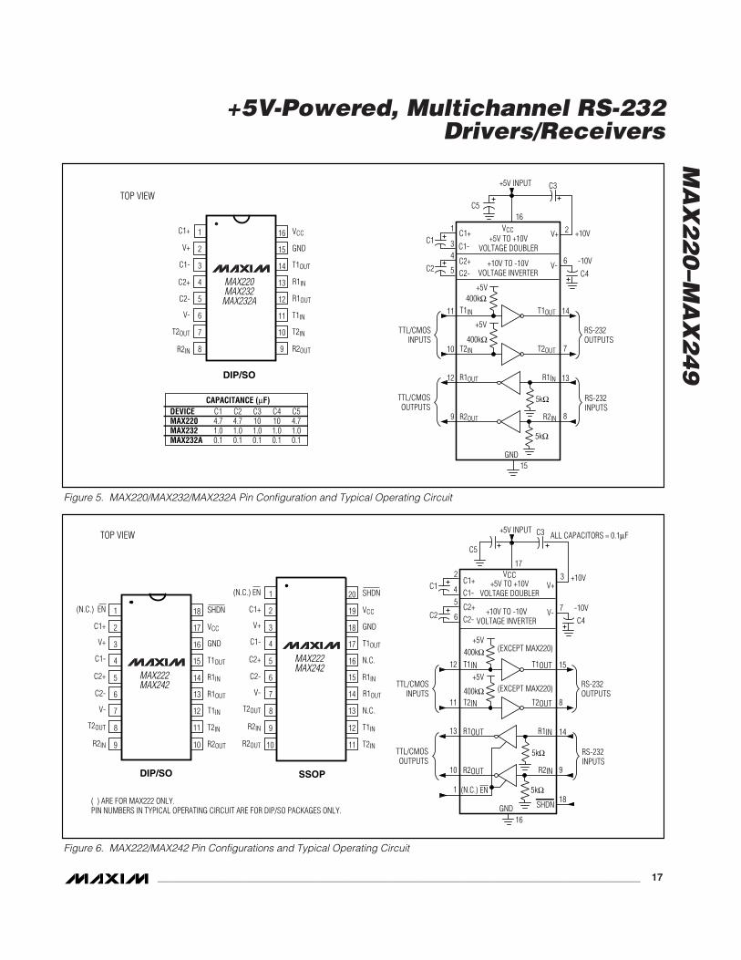
MA
X2
20
–M
AX
24
9
+5V-Powered, Multichannel RS-232Drivers/Receivers
______________________________________________________________________________________ 17
TOP VIEW
16
15
14
13
12
11
10
9
1
2
3
4
5
6
7
8
VCC
GND
T1OUT
R1INC2+
C1-
V+
C1+
MAX220
MAX232
MAX232A R1OUT
T1IN
T2IN
R2OUTR2IN
T2OUT
V-
C2-
DIP/SO
V+
V-
2 +10VC1+C1
C2
1
3
4
5
11
10
12
9
6
14
7
13
8
T1IN
R1OUT
T2IN
R2OUT
T1OUT
R1IN
T2OUT
R2IN
+5V INPUT
C2+ -10V
C4
RS-232OUTPUTS
RS-232INPUTS
TTL/CMOSINPUTS
TTL/CMOSOUTPUTS
GND
15
5kΩ
5kΩ
400kΩ
400kΩ
+5V
+5V
+10V TO -10VVOLTAGE INVERTER
+5V TO +10VVOLTAGE DOUBLER
16
C3
C5
CAPACITANCE (µF)
DEVICEMAX220MAX232MAX232A
C14.71.00.1
C24.71.00.1
C3101.00.1
C4101.00.1
C54.71.00.1
C2-
C1-
VCC
5kΩ
DIP/SO
18
17
16
15
14
13
12
11
1
2
3
4
5
6
7
8
SHDN
VCC
GND
T1OUTC1-
V+
C1+
(N.C.) EN
R1IN
R1OUT
T1IN
T2INT2OUT
V-
C2-
C2+
109 R2OUTR2IN
MAX222
MAX242
20
19
18
17
16
15
14
13
1
2
3
4
5
6
7
8
SHDN
VCC
GND
T1OUTC1-
V+
C1+
(N.C.) EN
N.C.
R1IN
R1OUT
N.C.T2OUT
V-
C2-
C2+
12
11
9
10
T1IN
T2INR2OUT
R2IN
MAX222
MAX242
SSOP
( ) ARE FOR MAX222 ONLY.PIN NUMBERS IN TYPICAL OPERATING CIRCUIT ARE FOR DIP/SO PACKAGES ONLY.
V+
V-
3 +10VC1
C2
2
4
5
6
12
11
13
7
15
8
14
9
T1IN
R1OUT
T2IN
R2OUT
T1OUT
(EXCEPT MAX220)
(EXCEPT MAX220)
R1IN
T2OUT
R2IN
+5V INPUT
C2+ -10V
C4
RS-232OUTPUTS
RS-232INPUTS
TTL/CMOSINPUTS
TTL/CMOSOUTPUTS
GND
16
5kΩ
400kΩ
400kΩ
+5V
+5V
+10V TO -10VVOLTAGE INVERTER
VCC+5V TO +10V
VOLTAGE DOUBLER
17
C3
C5
1
10
18SHDN
EN(N.C.)
ALL CAPACITORS = 0.1µF
C2-
C1+
C1-
TOP VIEW
Figure 5. MAX220/MAX232/MAX232A Pin Configuration and Typical Operating Circuit
Figure 6. MAX222/MAX242 Pin Configurations and Typical Operating Circuit

MA
X2
20
–M
AX
24
9
+5V-Powered, Multichannel RS-232Drivers/Receivers
18 ______________________________________________________________________________________
13
14
28
27
26
25
24
23
22
21
1
2
3
4
5
6
7
8
VCC
VCC VCC
400kΩ
400kΩ
400kΩ
400kΩ
400kΩ
T1OUT+5V
+5V
0.1
+5V
3
28 27
4
25
24
23
26
5
6
7
22
GNDENR
ENR
GND
21
+5V
+5V
+5V
T2OUT
T3OUT
T4OUT
5kΩ
5kΩ
5kΩ
5kΩ
5kΩ
1413
2
1
T5OUT
T5OUT
R1IN
R2IN
R3IN
R4IN
R5IN
T1IN11
12
18
17
16
15
10
9
8
19
20
T2IN
T3IN
T4IN
T5IN
ENT
R2OUT
R3OUT
R4OUT
PINS (ENR, GND, VCC, T5OUT) ARE INTERNALLY CONNECTED.
CONNECT EITHER OR BOTH EXTERNALLY. T5OUT IS A SINGLE DRIVER.
R5OUT
R1OUT
VCC
ENT
T3INT2IN
T1IN
ENR
ENR
T4IN
T5IN
R4OUT
R5OUTR3IN
R3OUT
R2OUT
R1OUT
20
19
18
17
9
10
11
12
R5IN
R4IN
T3OUT
T4OUTT2OUT
T1OUT
R1IN
R2IN
SO
MAX225
16
15
T5OUT
MAX225 FUNCTIONAL DESCRIPTION
5 RECEIVERS
5 TRANSMITTERS
2 CONTROL PINS
1 RECEIVER ENABLE (ENR)
1 TRANSMITTER ENABLE (ENT)
T5OUTGND
GND
TOP VIEW
Figure 7. MAX225 Pin Configuration and Typical Operating Circuit

MA
X2
20
–M
AX
24
9
+5V-Powered, Multichannel RS-232Drivers/Receivers
______________________________________________________________________________________ 19
GND
10
27R3OUT
23R4OUT
R3IN
R4IN
5kΩ
5kΩ
5 4R2OUT R2IN
5kΩ
RS-232INPUTS
LOGICOUTPUTS
RS-232OUTPUTS
TTL/CMOSINPUTS
R2
8 9R1OUT R1IN
5kΩ
R1
R3
R4
19 18R5OUT R5IN
5kΩ
R5
27 T1IN T1OUT
+5V
400kΩ
+5V
6 3T2IN T2OUTT2
400kΩ
20 T3OUT 1T3IN
+5V
T3
400kΩ
C1+
C1-
1.0µF
12VCC
+5V INPUT
11
17
1.0µF
131.0µF
+5V TO +10VVOLTAGE DOUBLER
26
1.0µF
T1
2821 T4IN T4OUT
+5V
400kΩ
T4
14
C2+
C2-
15
1.0µF 16
+10V TO -10VVOLTAGE INVERTER
V+
22
EN (EN)2425
28
27
26
25
24
23
22
21
20
19
18
17
16
15
1
2
3
4
5
6
7
8
9
10
11
12
13
14
T4OUT
R3IN
R3OUT
SHDN (SHDN)
R4IN*
C2+
R4OUT*
T4IN
T3IN
R5OUT*
R5IN*
V-
C2-
C1-
V+
C1+
VCC
GND
R1IN
R1OUT
T1IN
T2IN
R2OUT
R2IN
T2OUT
T1OUT
T3OUT
Wide SO/SSOP
MAX223
MAX241
EN (EN)
SHDN(SHDN)
*R4 AND R5 IN MAX223 REMAIN ACTIVE IN SHUTDOWN
NOTE: PIN LABELS IN ( ) ARE FOR MAX241
V-
TOP VIEW
Figure 8. MAX223/MAX241 Pin Configuration and Typical Operating Circuit

MA
X2
20
–M
AX
24
9
+5V-Powered, Multichannel RS-232Drivers/Receivers
20 ______________________________________________________________________________________
20
19
18
17
16
15
14
13
1
2
3
4
5
6
7
8
T5IN
N.C.
SHDNT2IN
T2OUT
T1OUT
T5OUT
T4IN
T3IN
V-C1+
VCC
GND
T1IN
12
11
9
10
C2-
C2+C1-
V+
DIP/SO
MAX230
V+
V-
9C1+
C1-
8
10
11
12
5
4
14
13
2
3
1
20
T3IN
T4IN
T2IN
T5IN
T1OUT
T2OUT
+5V INPUT
C2+
C2-
RS-232OUTPUTS
TTL/CMOSINPUTS
GND
6
400kΩ+5V
400kΩ
+5V
400kΩ
+5V
400kΩ+5V
400kΩ
+5V
+10V TO -10VVOLTAGE INVERTER
VCC+5V TO +10V
VOLTAGE DOUBLER
7
1.0µF
1.0µF
1.0µF
1.0µF
19
15
16
T3OUT T4OUT
18x
T1IN
T3OUT
T4OUT
T5OUT
17
1.0µF
T2
T3
T4
T5
N.C. SHDN
T1
TOP VIEW
Figure 9. MAX230 Pin Configuration and Typical Operating Circuit
V+
V-
14C1+
C1-
1
2
8
7
3
11
4T2IN
T1IN T1OUT
T2OUT
+5V INPUT
RS-232INPUTS
TTL/CMOSOUTPUTS
GND
12 (14)
5kΩ
5kΩ
+12V TO -12VVOLTAGE CONVERTER
13 (15)
1.0µF
1.0µF
C21.0µF
400kΩ
+5V
400kΩ
+5V
6
9 10R1IN
R2INR2OUT
R1OUT
5
16
15
14
13
12
11
10
9
1
2
3
4
5
6
7
8
V+
VCC
GND
T1OUTT2OUT
V-
C-
C+
MAX231
R1IN
R1OUT
T1IN
N.C.N.C.
T2IN
R2OUT
R2IN
SO
(12)
RS-232OUTPUTS
TTL/CMOSINPUTS
(11)
(13)(10)
VCC
PIN NUMBERS IN ( ) ARE FOR SO PACKAGE
14
13
12
11
10
9
8
1
2
3
4
5
6
7
V+
VCC
GND
T1OUTT2OUT
V-
C-
C+
MAX231
R1IN
R1OUT
T1INT2IN
R2OUT
R2IN
DIP
+7.5V TO +12V
(16)
T1
T2
R1
R2
TOP VIEW
Figure 10. MAX231 Pin Configurations and Typical Operating Circuit

MA
X2
20
–M
AX
24
9
+5V-Powered, Multichannel RS-232Drivers/Receivers
______________________________________________________________________________________ 21
2
1
5
18T2IN
T1IN T1OUT
T2OUT
+5V INPUT
RS-232OUTPUTS
TTL/CMOSOUTPUTS
GND GND
6 9
400kΩ
+5V
400kΩ
+5V
5kΩ
5kΩ
7
20
3 4R1IN
R2INR2OUT
R1OUT
19
RS-232OUTPUTS
TTL/CMOSINPUTS
VCC
( ) ARE FOR SO PACKAGE ONLY.
20
19
18
17
16
15
14
13
1
2
3
4
5
6
7
8
R2IN
T2OUT
V-R1IN
R1OUT
T1IN
C2-
C2+
V+ (C1-)
C1- (C1+)(V+) C1+
VCC
GND
T1OUT
12
11
9
10
V- (C2+)
C2+ (C2-)(V-) CS-
GND
DIP/SO
MAX233
MAX233A
T2IN R2OUT
C1+
C1-
V-
V-
V+
C2+
C2-
C2-
C2+
8 (13)
13 (14)
12 (10)
17
14 (8)
11 (12)
15
16
10 (11)
DO NOT MAKECONNECTIONS TO
THESE PINS
INTERNAL -10POWER SUPPLY
INTERNAL +10VPOWER SUPPLY
1.0µF
TOP VIEW
Figure 11. MAX233/MAX233A Pin Configuration and Typical Operating Circuit
16
15
14
13
12
11
10
9
1
2
3
4
5
6
7
8
T3OUT
T4OUT
T4IN
T3INT1IN
T2IN
T2OUT
T1OUT
MAX234
V-
C2-
C2+
C1-V+
C1+
VCC
GND
DIP/SO
V+
V-
8C1+
C1-
1.0µF
1.0µF
1.0µF
7
9
10
11
4
3
13
14
12
1
3
16
15
T1IN
T3IN
T2IN
T4IN
T1OUT
T3OUT
T2OUT
T4OUT
+5V INPUT
C2-
C2+
RS-232OUTPUTS
TTL/CMOSINPUTS
GND
5
+5V
+5V
+10V TO -10VVOLTAGE INVERTER
VCC
+5V TO +10VVOLTAGE DOUBLER
6
+5V
+5V
400kΩ
400kΩ
400kΩ
400kΩ
1.0µF
1.0µF
T1
T2
T4
T3
TOP VIEW
Figure 12. MAX234 Pin Configuration and Typical Operating Circuit

MA
X2
20
–M
AX
24
9
+5V-Powered, Multichannel RS-232Drivers/Receivers
22 ______________________________________________________________________________________
1.0µF
+5V INPUT
GND
11
6
23
5R2OUT
RS-232INPUTS
TTL/CMOSOUTPUTS
14 13
21
R5OUT
5kΩ
17 18R4OUT
5kΩ
24R3OUT
5kΩ
24
23
22
21
20
19
18
17
1
2
3
4
5
6
7
8
R3IN
R3OUT
T5IN
SHDNT2OUT
T1OUT
T3OUT
T4OUT
EN
T5OUT
R4IN
R4OUTT1IN
T2IN
R2OUT
R2IN
16
15
14
13
9
10
11
12
T4IN
T3IN
R5OUT
R5INVCC
GND
R1IN
R1OUT
DIP
MAX235
5kΩ
9 10R1OUT R1IN
R2IN
R3IN
R4IN
R5IN
5kΩ
7
15
3
4T2IN
T3OUT RS-232OUTPUTS
TTL/CMOSINPUTS
22 19T5IN T5OUT
+5V
16 1T4IN T4OUT
+5V
2T3IN
+5V
+5V
8 T1IN T1OUT
+5V
T2OUT
T1
T1
R2
R3
R4
R5
T2
T3
T5
T4
400kΩ
400kΩ
400kΩ
400kΩ
400kΩ
SHDNEN20
12
VCC
TOP VIEW
Figure 13. MAX235 Pin Configuration and Typical Operating Circuit

MA
X2
20
–M
AX
24
9
+5V-Powered, Multichannel RS-232Drivers/Receivers
______________________________________________________________________________________ 23
GND
8
23R2OUT RS-232INPUTS
TTL/CMOSOUTPUTS
17 16
21
R3OUT
R2IN
R3IN
5kΩ
5kΩ
5 4R1OUT R1IN
5kΩ
RS-232OUTPUTS
TTL/CMOSINPUTS
R1
R2
R3
27 T1IN T1OUT
+5V
T1
400kΩ
6 3T2IN
+5V
T2OUTT2
400kΩ
18 T3OUT 1T3IN
+5V
T3
400kΩ
19 24T4IN T4OUT
+5V
T4
400kΩ
SHDNEN20
11C1+
C1-
1.0µF
10
12
13
14
15
+5V INPUT
C2+
C2-
VCC
+5V TO +10VVOLTAGE DOUBLER
9 1.0µF
1.0µF+10V TO -10V
VOLTAGE INVERTER
22
24
23
22
21
20
19
18
17
1
2
3
4
5
6
7
8
T4OUT
R2IN
R2OUT
SHDNR1IN
T2OUT
T1OUT
T3OUT
T4IN
T3IN
R3OUTGND
T1IN
T2IN
R1OUT
16
15
14
13
9
10
11
12
R3IN
V-
C2-
C2+C1-
V+
C1+
VCC
DIP/SO
MAX236 EN
1.0µF
1.0µF
TOP VIEW
V+
V-
Figure 14. MAX236 Pin Configuration and Typical Operating Circuit

MA
X2
20
–M
AX
24
9
+5V-Powered, Multichannel RS-232Drivers/Receivers
24 ______________________________________________________________________________________
GND
8
23R2OUT RS-232INPUTS
TTL/CMOSOUTPUTS
17 16R3OUT
R2IN
R3IN
5kΩ
5kΩ
5 4R1OUT R1IN
5kΩ
RS-232OUTPUTS
TTL/CMOSINPUTS
R1
R2
R3
27 T1IN T1OUT
+5V
T1
400kΩ
6 3T2IN
+5V
T2OUTT2
400kΩ
18 T3OUT 1T3IN
+5V
T3
400kΩ
21 20T5IN T5OUT
+5V
T5
400kΩ
11C1+
C1-
1.0µF
10
12
13
14
15
+5V INPUT
C2+
C2-
VCC
+5V TO +10VVOLTAGE DOUBLER
9 1.0µF
1.0µF+10V TO -10V
VOLTAGE INVERTER
22
24
23
22
21
20
19
18
17
1
2
3
4
5
6
7
8
T4OUT
R2IN
R2OUT
T5INR1IN
T2OUT
T1OUT
T3OUT
T4IN
T3IN
R3OUTGND
T1IN
T2IN
R1OUT
16
15
14
13
9
10
11
12
R3IN
V-
C2-
C2+C1-
V+
C1+
VCC
DIP/SO
MAX237 T5OUT
1.0µF
1.0µF
19 24T4IN T4OUT
+5V
T4
400kΩ
V+
V-
TOP VIEW
Figure 15. MAX237 Pin Configuration and Typical Operating Circuit
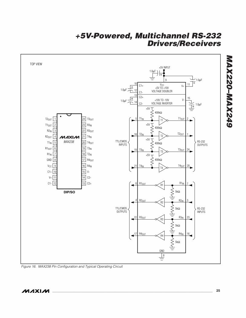
MA
X2
20
–M
AX
24
9
+5V-Powered, Multichannel RS-232Drivers/Receivers
______________________________________________________________________________________ 25
GND
8
3R2OUT
22 23R3OUT
R2IN
R3IN
5kΩ
5kΩ
6 7R1OUT R1IN
5kΩ
RS-232OUTPUTS
TTL/CMOSINPUTS
RS-232INPUTS
TTL/CMOSOUTPUTS
R1
R2
R3
17 16R4OUT R4IN
5kΩ
R4
25 T1IN T1OUT
+5V
400kΩ
+5V
18 1T2IN T2OUTT2
400kΩ
19 T3OUT 24T3IN
+5V
T3
400kΩ
11C1+
C1-
1.0µF
10
12
13
14
15
+5V INPUT
C2+
C2-
VCC
+5V TO +10VVOLTAGE DOUBLER
9 1.0µF
1.0µF
+10V TO -10VVOLTAGE INVERTER
4
1.0µF
1.0µF
21 20T4IN T4OUT
+5V
T4
400kΩ
T124
23
22
21
20
19
18
17
1
2
3
4
5
6
7
8
T3OUT
R3IN
R3OUT
T4INR2OUT
R2IN
T1OUT
T2OUT
TOP VIEW
T3IN
T2IN
R4OUTGND
R1IN
R1OUT
T1IN
16
15
14
13
9
10
11
12
R4IN
V-
C2-
C2+C1-
V+
C1+
VCC
DIP/SO
MAX238 T4OUT
V+
V-
Figure 16. MAX238 Pin Configuration and Typical Operating Circuit

MA
X2
20
–M
AX
24
9
+5V-Powered, Multichannel RS-232Drivers/Receivers
26 ______________________________________________________________________________________
GND
3
18R3OUT
12R4OUT
R3IN
R4IN
5kΩ
5kΩ
22 21R2OUT R2IN
5kΩ
RS-232OUTPUTS
TTL/CMOSINPUTS
RS-232INPUTS
TTL/CMOSOUTPUTS
R2
1 2R1OUT R1IN
5kΩ
R1
R3
R4
10 9R5OUT R5IN
5kΩ
R5
1924 T1IN T1OUT
+5V
400kΩ
+5V
23 20T2IN T2OUTT2
400kΩ
16 T3OUT 13T3IN
+5V
T3
400kΩ
C1+
C1-
1.0µF
6 VCC8
+5V INPUT
4 5
1.0µF+10V TO -10V
VOLTAGE INVERTER
17
1.0µF
T1
24
23
22
21
20
19
18
17
1
2
3
4
5
6
7
8
T1IN
T2IN
R2OUT
R2INVCC
GND
R1IN
R1OUT
T1OUT
R3IN
R3OUTV-
C-
C+
V+
16
15
14
13
9
10
11
12
T3IN
N.C.
EN
T3OUTR4IN
R4OUT
R5OUT
R5IN
DIP/SO
MAX239 T2OUT
7.5V TO 13.2VINPUT
7
V+
11
EN14 15N.C.
V-
TOP VIEW
Figure 17. MAX239 Pin Configuration and Typical Operating Circuit

MA
X2
20
–M
AX
24
9
+5V-Powered, Multichannel RS-232Drivers/Receivers
______________________________________________________________________________________ 27
GND
18
4R3OUT
40R4OUT
R3IN
R4IN
5kΩ
5kΩ
13 10R2OUT R2IN
5kΩ
RS-232INPUTS
TTL/CMOSOUTPUTS
RS-232OUTPUTS
TTL/CMOSINPUTS
R2
16 17R1OUT R1IN
5kΩ
R1
R3
R4
36 35R5OUT R5IN
5kΩ
R5
715 T1IN T1OUT
+5V400kΩ
+5V
14 8T2IN T2OUTT2
400kΩ
37 T3OUT 6T3IN
+5V
T3
400kΩ
C1+
C1-
1.0µF
25VCC
+5V INPUT
19
30
1.0µF
26
1.0µF
+5V TO +10VVOLTAGE DOUBLER
3
1.0µF
T1
+5V
2 41T5IN T5OUTT5
400kΩ
538 T4IN T4OUT
+5V400kΩ
T4
27
C2+
C2-
28
1.0µF 29
+5V TO -10VVOLTAGE INVERTER
V+
39
EN42 43
Plastic FP
MAX240
SHDN
EN
T5OUT
R4IN
R4OUT
R5OUT
R5IN
N.C.
N.C.
T3IN
T4IN
R2OUT
T2IN
T1IN
R1OUT
R1IN
N.C.
N.C.
N.C.
N.C.
VCC
GND
R2 I
N
N.C
.
T4O
UT
T2O
UT
T1O
UT
T3O
UT
N.C
.
R3 I
N
R3 O
UT
N.C
.
T5IN
N.C
.
C1+ C
2
V+
C1-
C2+
N.C
.
V-
N.C
.
N.C
.
N.C
.
3332313029282726252423
34
35
36
37
38
39
40
41
42
43
44
1234567891011
22
21
20
19
18
17
16
15
14
13
12
SHDN
TOP VIEW
V-
Figure 18. MAX240 Pin Configuration and Typical Operating Circuit
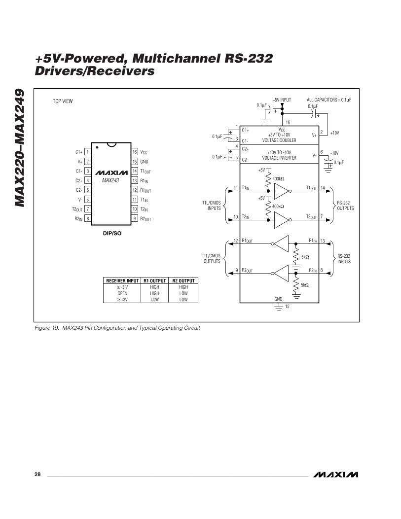
MA
X2
20
–M
AX
24
9
+5V-Powered, Multichannel RS-232Drivers/Receivers
28 ______________________________________________________________________________________
V+
V-
2 +10VC1+
C1-
1
3
4
5
11
10
12
9
6
14
7
13
8
T1IN
R1OUT
T2IN
R2OUT
T1OUT
R1IN
T2OUT
R2IN
+5V INPUT
C2+
C2-
-10V
RS-232OUTPUTS
RS-232INPUTS
TTL/CMOSINPUTS
TTL/CMOSOUTPUTS
GND
15
5kΩ
5kΩ
400kΩ
400kΩ
+5V
+5V
+10V TO -10VVOLTAGE INVERTER
+5V TO +10VVOLTAGE DOUBLER
16
16
15
14
13
12
11
10
9
1
2
3
4
5
6
7
8
C1+ VCC
GND
T1OUT
R1IN
R1OUT
T1IN
T2IN
R2OUT
MAX243
DIP/SO
V+
C1-
V-
C2+
C2-
T2OUT
R2IN
0.1µF
0.1µF
0.1µF
0.1µF
ALL CAPACITORS = 0.1µF
0.1µF
RECEIVER INPUT
≤ -3 V
OPEN
≥ +3V
R1 OUTPUT
HIGH
HIGH
LOW
R2 OUTPUT
HIGH
LOW
LOW
TOP VIEW
VCC
Figure 19. MAX243 Pin Configuration and Typical Operating Circuit

MA
X2
20
–M
AX
24
9
+5V-Powered, Multichannel RS-232Drivers/Receivers
______________________________________________________________________________________ 29
400kΩ
+10V TO -10V VOLTAGE INVERTER
+5V TO +10V VOLTAGE DOUBLER
VCC
400kΩ
400kΩ
GND
+5V +5V
+5V +5V
+5V
25
24
23
2120
2
1µF
1µF
1µF 1µF
1µF
16
3
17
4
18
5kΩ
5kΩ
5kΩ
5kΩ
5kΩ
5kΩ
5kΩ
5kΩ
5kΩ
5kΩ
C2-
C2+
C1-
C1+
TA2OUT
TA2IN
TA3OUT
TA3IN
TA4OUT
TA4IN
9 RA1IN
10 RA1OUT
8 RA2IN
11 RA2OUT
7 RA3IN
12 RA3OUT
6 RA4IN
13 RA4OUT
5 RA5IN
14
19
RA5OUT
26
22
43
29
42
28
41
27
36
35
37
34
38
33
39
32
40
31
V-
V+
TB2OUT
TB2IN
400kΩ
2
15
TA1OUT
TA1IN
44
30
TB1OUT
TB1IN
TB3OUT
TB3IN
TB4OUT
TB4IN
RB1IN
RB1OUT
RB2IN
RB2OUT
RB3IN
RB3OUT
RB4IN
RB4OUT
RB5IN
RB5OUT
MAX249 FUNCTIONAL DESCRIPTION
10 RECEIVERS
5 A-SIDE RECEIVER
5 B-SIDE RECEIVER
8 TRANSMITTERS
4 A-SIDE TRANSMITTERS
4 B-SIDE TRANSMITTERS
NO CONTROL PINS
441234 404142435
21 24 2625 27 2822 2319 20
8
9
10
11
12
13
14
15
16
17 29
30
31
32
33
34
35
36
37
38
TA3IN
VC
C
RA
5IN
MAX244
PLCC
TOP VIEWT A
4OU
T
T A3O
UT
T A2O
UT
T A1O
UT
T B1O
UT
T B2O
UT
T B3O
UT
TB4O
UT
RB
5IN
GN
D V+
C1+
C2+C1- V-
C2-
T B3I
N
T B4I
N
RB3IN
RB2IN
RB1IN
RB1OUT
RB2OUT
RB3OUT
RB4OUT
RB5OUT
TB1IN
TB2IN
TA2IN
TA1IN
RA5OUT
RA4OUT
RA3OUT
RA2OUT
RA1OUT
RA1IN
RA2IN
7 39 RB4INRA3IN
6
18
RA
4IN
T A4I
N
+5V +5V
+5V +5V
Figure 20. MAX244 Pin Configuration and Typical Operating Circuit

MA
X2
20
–M
AX
24
9
+5V-Powered, Multichannel RS-232Drivers/Receivers
30 ______________________________________________________________________________________
400kΩ
VCC
400kΩ
400kΩ
GND
+5V +5V
+5V +5V
+5V
40
17
1µF
3
18
4
19
5
5kΩ
5kΩ
5kΩ
5kΩ
5kΩ
5kΩ
5kΩ
5kΩ
5kΩ
5kΩ
TA2OUT
TA2IN
TA3OUT
TA3IN
TA4OUT
TA4IN
1
11 RA1IN
10 RA1OUT
12 RA2IN
9 RA2OUT
13 RA3IN
8 RA3OUT
14 RA4IN
7 RA4OUT
15 RA5IN
6
20
RA5OUT
23
37
22
36
21
35
29
30
28
31
27
32
26
33
25
34
TB2OUT
TB2IN
TB3OUT
TB3IN
TB4OUT
TB4IN
RB1IN
RB1OUT
RB2IN
RB2OUT
RB3IN
RB3OUT
RB4IN
RB4OUT
RB5IN
RB5OUT
+5V +5V
400kΩ
16
2
TA1OUT
TA1IN
24
38
TB1OUT
TB1IN
+5V +5V40 VCC
ENT
TB1IN
TB2IN
TB3IN
TB4IN
RB5OUT
RB4OUT
RB3OUT
RB2OUT
RB1OUT
RB1IN
RB2IN
RB3IN
RB4IN
RB5IN
TB1OUT
TB2OUT
TB3OUT
TB4OUT
39
38
37
36
35
34
33
32
31
1
2
3
4
5
6
7
8
9
10
ENR
TA1IN
TA2IN
TA3IN
TA4IN
RA5OUT
RA4OUT
RA3OUT
RA2OUT
RA1OUT
RA1IN
RA2IN
RA3IN
RA4IN
RA5IN
TA1OUT
TA2OUT
TA3OUT
TA4OUT
GND
TOP VIEW
MAX245
30
29
28
27
26
25
24
23
22
21
11
12
13
14
15
16
17
18
19
DIP
20
MAX245 FUNCTIONAL DESCRIPTION
10 RECEIVERS
5 A-SIDE RECEIVERS (RA5 ALWAYS ACTIVE)
5 B-SIDE RECEIVERS (RB5 ALWAYS ACTIVE)
8 TRANSMITTTERS
4 A-SIDE TRANSMITTERS
2 CONTROL PINS
1 RECEIVER ENABLE (ENR)
1 TRANSMITTER ENABLE (ENT)
39ENR ENT
Figure 21. MAX245 Pin Configuration and Typical Operating Circuit

MA
X2
20
–M
AX
24
9
+5V-Powered, Multichannel RS-232Drivers/Receivers
______________________________________________________________________________________ 31
400kΩ
VCC
400kΩ
GND
+5V
+5V
+5V
+5V
+5V
40
16
1µF
2
18
4
TA1OUT
TA1IN
TA3OUT
TA3IN
20
24
38
22
36
1 39
TB1OUT
TB1IN
TB3OUT
TB3IN
400kΩ
+5V
17
3
TA2OUT
TA2IN
+5V
23
37
TB2OUT
TB2IN
400kΩ
+5V
19
5
TA4OUT
TA4IN
+5V
21
35
TB4OUT
TB4IN
5kΩ
5kΩ
5kΩ
5kΩ
5kΩ
5kΩ
5kΩ
5kΩ
5kΩ
5kΩ
11 RA1IN
10 RA1OUT
12 RA2IN
9 RA2OUT
13 RA3IN
8 RA3OUT
14 RA4IN
7 RA4OUT
15 RA5IN
6 RA5OUT
29
30
28
31
27
32
26
33
25
34
RB1IN
RB1OUT
RB2IN
RB2OUT
RB3IN
RB3OUT
RB4IN
RB4OUT
RB5IN
RB5OUT
40 VCC
ENB
TB1IN
TB2IN
TB3IN
TB4IN
RB5OUT
RB4OUT
RB3OUT
RB2OUT
RB1OUT
RB1IN
RB2IN
RB3IN
RB4IN
RB5IN
TB1OUT
TB2OUT
TB3OUT
TB4OUT
39
38
37
36
35
34
33
32
31
1
2
3
4
5
6
7
8
9
10
ENA
TA1IN
TA2IN
TA3IN
TA4IN
RA5OUT
RA4OUT
RA3OUT
RA2OUT
RA1OUT
RA1IN
RA2IN
RA3IN
RA4IN
RA5IN
TA1OUT
TA2OUT
TA3OUT
TA4OUT
GND
TOP VIEW
MAX246
30
29
28
27
26
25
24
23
22
21
11
12
13
14
15
16
17
18
19
DIP
20
MAX246 FUNCTIONAL DESCRIPTION
10 RECEIVERS
5 A-SIDE RECEIVERS (RA5 ALWAYS ACTIVE)
5 B-SIDE RECEIVERS (RB5 ALWAYS ACTIVE)
8 TRANSMITTERS
4 A-SIDE TRANSMITTERS
4 B-SIDE TRANSMITTERS
2 CONTROL PINS
ENABLE A-SIDE (ENA)
ENABLE B-SIDE (ENB)
ENA ENB
Figure 22. MAX246 Pin Configuration and Typical Operating Circuit
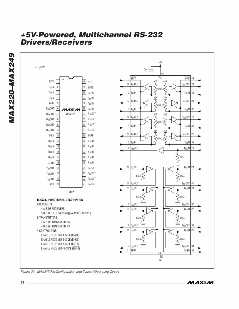
MA
X2
20
–M
AX
24
9
+5V-Powered, Multichannel RS-232Drivers/Receivers
32 ______________________________________________________________________________________
400kΩ
VCC
400kΩ
GND
+5V
+5V
+5V
+5V
+5V
1
40
16
1µF
2
18
4
5kΩ
5kΩ
5kΩ
5kΩ
5kΩ
5kΩ
5kΩ
5kΩ
ENTA
TA1OUT
TA1IN
TA3OUT
TA3IN
6 RB5OUT
12 RA1IN
10 RA1OUT
13 RA2IN
9 RA2OUT
14 RA3IN
8 RA3OUT
15 RA4IN
7
20
RA4OUT
11
39
24
38
22
36
29
31
28
32
27
33
26
34
30ENRA
ENTB
TB1OUT
TB1IN
TB3OUT
TB3IN
RB1IN
5kΩ
25RB5IN
RB1OUT
RB2IN
RB2OUT
RB3IN
RB3OUT
RB4IN
RB4OUT
ENRB
400kΩ
+5V
17
3
TA2OUT
TA2IN
+5V
23
37
TB2OUT
TB2IN
400kΩ
+5V
19
5
TA4OUT
TA4IN
+5V
21
35
TB4OUT
TB4IN
40 VCC
ENTB
TB1IN
TB2IN
TB3IN
TB4IN
RB4OUT
RB3OUT
RB2OUT
RB1OUT
RB1IN
RB2IN
RB3IN
RB4IN
RB5IN
TB1OUT
TB2OUT
TB3OUT
TB4OUT
39
38
37
36
35
34
33
32
31
1
2
3
4
5
6
7
8
9
10
ENTA
TA1IN
TA2IN
TA3IN
TA4IN
RB5OUT
RA4OUT
RA3OUT
RA2OUT
RA1OUT
RA1IN
RA2IN
RA3IN
RA4IN
TA1OUT
TA2OUT
TA3OUT
TA4OUT
GND
TOP VIEW
MAX247
30
29
28
27
26
25
24
23
22
21
11
12
13
14
15
16
17
18
19
DIP
20
ENRA ENRB
MAX247 FUNCTIONAL DESCRIPTION
9 RECEIVERS
4 A-SIDE RECEIVERS
5 B-SIDE RECEIVERS (RB5 ALWAYS ACTIVE)
8 TRANSMITTERS
4 A-SIDE TRANSMITTERS
4 B-SIDE TRANSMITTERS
4 CONTROL PINS
ENABLE RECEIVER A-SIDE (ENRA)
ENABLE RECEIVER B-SIDE (ENRB)
ENABLE RECEIVER A-SIDE (ENTA)
ENABLE RECEIVERr B-SIDE (ENTB)
Figure 23. MAX247 Pin Configuration and Typical Operating Circuit

MA
X2
20
–M
AX
24
9
+5V-Powered, Multichannel RS-232Drivers/Receivers
______________________________________________________________________________________ 33
400kΩ
+10V TO -10V VOLTAGE INVERTER
+5V TO +10V VOLTAGE DOUBLER
VCC
400kΩ
GND
+5V
+5V
+5V
+5V
+5V
18
25
24
23
2120
1
1µF
1µF
1µF1µF
1µF
14
3
16
5kΩ
5kΩ
5kΩ
5kΩ
5kΩ
5kΩ
5kΩ
5kΩ
ENTA
C2-
C2+
C1-
C1+
TA1OUT
TA1IN
TA3OUT
TA3IN
8 RA1IN
10 RA1OUT
7 RA2IN
11 RA2OUT
6 RA3IN
12 RA3OUT
5 RA4IN
13
19
RA4OUT
9
27
26
22
44
31
42
29
37
35
38
34
39
33
40
32
36ENRA
ENTB
V-
V+
TB1OUT
TB1IN
TB3OUT
TB3IN
RB1IN
RB1OUT
RB2IN
RB2OUT
RB3IN
RB3OUT
RB4IN
RB4OUT
ENRB
400kΩ
+5V
2
15
TA2OUT
TA2IN
+5V
43
30
TB2OUT
TB2IN
400kΩ
+5V
4
17
TA4OUT
TA4IN
+5V
41
28
TB4OUT
TB4IN
441234 404142435
21 24 2625 27 2822 2319 20
8
9
10
11
12
13
14
15
16
17 29
30
31
32
33
34
35
36
37
38
TA4IN
VC
C
RA
4IN
MAX248
PLCC
TOP VIEWT A
4OU
T
T A3O
UT
T A2O
UT
T A1O
UT
T B1O
UT
T B2O
UT
T B3O
UT
T A4O
UT
RB
4IN
GN
D V+
C1+
C2+C1- V-
C2-
T B4I
N
ENTB
RB2IN
RB1IN
RB1OUT
RB2OUT
RB3OUT
RB4OUT
TB1IN
TB2IN
TB3IN
TA3IN
TA2IN
TA1IN
RA4OUT
RA3OUT
RA2OUT
RA1OUT
ENRA
RA1IN
7 39 RB3INRA2IN
6
18
RA
3IN
ENRB
ENTA
MAX248 FUNCTIONAL DESCRIPTION
8 RECEIVERS
4 A-SIDE RECEIVERS
4 B-SIDE RECEIVERS
8 TRANSMITTERS
4 A-SIDE TRANSMITTERS
4 B-SIDE TRANSMITTERS
4 CONTROL PINS
ENABLE RECEIVER A-SIDE (ENRA)
ENABLE RECEIVER B-SIDE (ENRB)
ENABLE RECEIVER A-SIDE (ENTA)
ENABLE RECEIVER B-SIDE (ENTB)
Figure 24. MAX248 Pin Configuration and Typical Operating Circuit
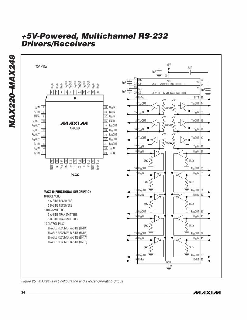
MA
X2
20
–M
AX
24
9
+5V-Powered, Multichannel RS-232Drivers/Receivers
34 ______________________________________________________________________________________
400kΩ
+10V TO -10V VOLTAGE INVERTER
+5V TO +10V VOLTAGE DOUBLER
VCC
400kΩ
400kΩ
GND
+5V
+5V
+5V
+5V
+5V
+5V
+5V
18
25
24
23
2120
1
1µF
1µF
1µF1µF
15
2
16
3
17
5kΩ
5kΩ
5kΩ
5kΩ
5kΩ
5kΩ
5kΩ
5kΩ
5kΩ
5kΩ
ENTA
C2-
C2+
C1-
C1+
TA1OUT
TA1IN
TA2OUT
TA2IN
TA3OUT
TA3IN
8 RA1IN
10 RA1OUT
7 RA2IN
11 RA2OUT
6 RA3IN
12 RA3OUT
5 RA4IN
13 RA4OUT
4 RA5IN
14
19
RA5OUT
9
27
26
22
44
30
43
29
42
28
37
35
38
34
39
33
40
32
41
31
36ENRA
ENTB
V-
V+
TB1OUT
TB1IN
TB2OUT
TB2IN
TB3OUT
TB3IN
RB1IN
RB1OUT
RB2IN
RB2OUT
RB3IN
RB3OUT
RB4IN
RB4OUT
RB5IN
RB5OUT
ENRB
441234 404142435
21 24 2625 27 2822 2319 20
8
9
10
11
12
13
14
15
16
17 29
30
31
32
33
34
35
36
37
38
VC
C
RA
4IN
RA
5IN
MAX249
PLCC
TOP VIEWT A
3OU
T
T A2O
UT
T A1O
UT
T B1O
UT
T B2O
UT
T B3O
UT
RB
4IN
RB
5IN
GN
D V+
C1+
C2+C1- V-
C2-
T B3I
N
ENTB
RB2IN
RB1IN
RB1OUT
MAX249 FUNCTIONAL DESCRIPTION
10 RECEIVERS
5 A-SIDE RECEIVERS
5 B-SIDE RECEIVERS
6 TRANSMITTERS
3 A-SIDE TRANSMITTERS
3 B-SIDE TRANSMITTERS
4 CONTROL PINS
ENABLE RECEIVER A-SIDE (ENRA)
ENABLE RECEIVER B-SIDE (ENRB)
ENABLE RECEIVER A-SIDE (ENTA)
ENABLE RECEIVER B-SIDE (ENTB)
RB2OUT
RB3OUT
RB4OUT
RB5OUT
TB1IN
TB2INTA3IN
TA2IN
TA1IN
RA4OUT
RA5OUT
RA3OUT
RA2OUT
RA1OUT
ENRA
RA1IN
7 39 RB3INRA2IN
6
18
RA
3IN
ENRB
ENTA
1µF
Figure 25. MAX249 Pin Configuration and Typical Operating Circuit
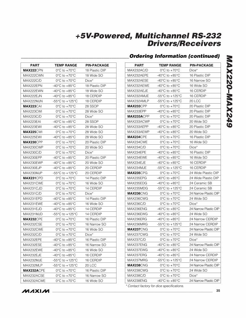
MA
X2
20
–M
AX
24
9
+5V-Powered, Multichannel RS-232Drivers/Receivers
______________________________________________________________________________________ 35
___________________________________________Ordering Information (continued)
PART
MAX222CPN 0°C to +70°C
TEMP RANGE PIN-PACKAGE PART TEMP RANGE PIN-PACKAGE
18 Plastic DIP
MAX222CWN 0°C to +70°C 18 Wide SO
MAX222C/D 0°C to +70°C Dice*
MAX222EPN -40°C to +85°C 18 Plastic DIP
MAX222EWN -40°C to +85°C 18 Wide SO
MAX222EJN -40°C to +85°C 18 CERDIP
MAX222MJN -55°C to +125°C 18 CERDIP
MAX223CAI 0°C to +70°C 28 SSOP
MAX223CWI 0°C to +70°C 28 Wide SO
MAX223C/D 0°C to +70°C Dice*
MAX223EAI -40°C to +85°C 28 SSOP
MAX223EWI -40°C to +85°C 28 Wide SO
MAX225CWI 0°C to +70°C 28 Wide SO
MAX225EWI -40°C to +85°C 28 Wide SO
MAX230CPP 0°C to +70°C 20 Plastic DIP
MAX230CWP 0°C to +70°C 20 Wide SO
MAX230C/D 0°C to +70°C Dice*
MAX230EPP -40°C to +85°C 20 Plastic DIP
MAX230EWP -40°C to +85°C 20 Wide SO
MAX230EJP -40°C to +85°C 20 CERDIP
MAX230MJP -55°C to +125°C 20 CERDIP
MAX231CPD 0°C to +70°C 14 Plastic DIP
MAX231CWE 0°C to +70°C 16 Wide SO
MAX231CJD 0°C to +70°C 14 CERDIP
MAX231C/D 0°C to +70°C Dice*
MAX231EPD -40°C to +85°C 14 Plastic DIP
MAX231EWE -40°C to +85°C 16 Wide SO
MAX231EJD -40°C to +85°C 14 CERDIP
MAX231MJD -55°C to +125°C 14 CERDIP
MAX232CPE 0°C to +70°C 16 Plastic DIP
MAX232CSE 0°C to +70°C 16 Narrow SO
MAX232CWE 0°C to +70°C 16 Wide SO
MAX232C/D 0°C to +70°C Dice*
MAX232EPE -40°C to +85°C 16 Plastic DIP
MAX232ESE -40°C to +85°C 16 Narrow SO
MAX232EWE -40°C to +85°C 16 Wide SO
MAX232EJE -40°C to +85°C 16 CERDIP
MAX232MJE -55°C to +125°C 16 CERDIP
MAX232MLP -55°C to +125°C 20 LCC
MAX232ACPE 0°C to +70°C 16 Plastic DIP
MAX232ACSE 0°C to +70°C 16 Narrow SO
MAX232ACWE 0°C to +70°C 16 Wide SO
MAX232AC/D
MAX232AEPE -40°C to +85°C 16 Plastic DIP
MAX232AESE
0°C to +70°C Dice*
-40°C to +85°C 16 Narrow SO
MAX232AEWE -40°C to +85°C 16 Wide SO
MAX232AEJE -40°C to +85°C 16 CERDIP
MAX232AMJE -55°C to +125°C 16 CERDIP
MAX232AMLP -55°C to +125°C 20 LCC
MAX233CPP 0°C to +70°C 20 Plastic DIP
MAX233EPP -40°C to +85°C 20 Plastic DIP
MAX233ACPP 0°C to +70°C 20 Plastic DIP
MAX233ACWP 0°C to +70°C 20 Wide SO
MAX233AEPP -40°C to +85°C 20 Plastic DIP
MAX233AEWP -40°C to +85°C 20 Wide SO
MAX234CPE 0°C to +70°C 16 Plastic DIP
MAX234CWE 0°C to +70°C 16 Wide SO
MAX234C/D 0°C to +70°C Dice*
MAX234EPE -40°C to +85°C 16 Plastic DIP
MAX234EWE -40°C to +85°C 16 Wide SO
MAX234EJE -40°C to +85°C 16 CERDIP
MAX234MJE -55°C to +125°C 16 CERDIP
MAX235CPG 0°C to +70°C 24 Wide Plastic DIP
MAX235EPG -40°C to +85°C 24 Wide Plastic DIP
MAX235EDG -40°C to +85°C 24 Ceramic SB
MAX235MDG -55°C to +125°C 24 Ceramic SB
MAX236CNG 0°C to +70°C 24 Narrow Plastic DIP
MAX236CWG 0°C to +70°C 24 Wide SO
MAX236C/D 0°C to +70°C Dice*
MAX236ENG -40°C to +85°C 24 Narrow Plastic DIP
MAX236EWG -40°C to +85°C 24 Wide SO
MAX236ERG -40°C to +85°C 24 Narrow CERDIP
MAX236MRG -55°C to +125°C 24 Narrow CERDIP
MAX237CNG 0°C to +70°C 24 Narrow Plastic DIP
MAX237CWG 0°C to +70°C 24 Wide SO
MAX237C/D 0°C to +70°C Dice*
MAX237ENG -40°C to +85°C 24 Narrow Plastic DIP
MAX237EWG -40°C to +85°C 24 Wide SO
MAX237ERG -40°C to +85°C 24 Narrow CERDIP
MAX237MRG -55°C to +125°C 24 Narrow CERDIP
MAX238CNG 0°C to +70°C 24 Narrow Plastic DIP
MAX238CWG 0°C to +70°C 24 Wide SO
MAX238C/D 0°C to +70°C Dice*
MAX238ENG -40°C to +85°C 24 Narrow Plastic DIP
* Contact factory for dice specifications.

MA
X2
20
–M
AX
24
9
+5V-Powered, Multichannel RS-232Drivers/Receivers
___________________________________________Ordering Information (continued)
* Contact factory for dice specifications.
18 CERDIP-55°C to +125°CMAX242MJN
18 CERDIP-40°C to +85°CMAX242EJN
18 Wide SO-40°C to +85°CMAX242EWN
18 Plastic DIP-40°C to +85°CMAX242EPN
Dice*0°C to +70°CMAX242C/D
18 Wide SO0°C to +70°CMAX242CWN
18 Plastic DIP0°C to +70°CMAX242CPN
20 SSOP0°C to +70°CMAX242CAP
28 Wide SO-40°C to +85°CMAX241EWI
28 SSOP-40°C to +85°CMAX241EAI
Dice*0°C to +70°CMAX241C/D
28 Wide SO0°C to +70°CMAX241CWI
28 SSOP0°C to +70°CMAX241CAI
Dice*0°C to +70°CMAX240C/D
44 Plastic FP0°C to +70°CMAX240CMH
24 Narrow CERDIP-55°C to +125°CMAX239MRG
24 Narrow CERDIP-40°C to +85°CMAX239ERG
24 Wide SO-40°C to +85°CMAX239EWG
24 Narrow Plastic DIP-40°C to +85°CMAX239ENG
Dice*0°C to +70°CMAX239C/D
24 Wide SO0°C to +70°CMAX239CWG
24 Narrow Plastic DIP0°C to +70°CMAX239CNG
24 Narrow CERDIP-55°C to +125°C
24 Wide SO
PIN-PACKAGETEMP RANGE
-40°C to +85°C
MAX238MRG
24 Narrow CERDIP-40°C to +85°CMAX238ERG
MAX238EWG
PART PIN-PACKAGETEMP RANGEPART
44 PLCC-40°C to +85°CMAX249EQH
44 PLCC0°C to +70°CMAX249CQH
44 PLCC-40°C to +85°CMAX248EQH
Dice*0°C to +70°CMAX248C/D
44 PLCC0°C to +70°CMAX248CQH
40 Plastic DIP-40°C to +85°CMAX247EPL
Dice*0°C to +70°CMAX247C/D
40 Plastic DIP0°C to +70°CMAX247CPL
40 Plastic DIP-40°C to +85°CMAX246EPL
Dice*0°C to +70°CMAX246C/D
40 Plastic DIP0°C to +70°CMAX246CPL
40 Plastic DIP-40°C to +85°CMAX245EPL
Dice*0°C to +70°CMAX245C/D
40 Plastic DIP0°C to +70°CMAX245CPL
44 PLCC-40°C to +85°CMAX244EQH
Dice*0°C to +70°CMAX244C/D
44 PLCC0°C to +70°CMAX244CQH
16 CERDIP-55°C to +125°CMAX243MJE
16 CERDIP-40°C to +85°CMAX243EJE
16 Wide SO-40°C to +85°CMAX243EWE
16 Narrow SO-40°C to +85°CMAX243ESE
16 Plastic DIP-40°C to +85°CMAX243EPE
Dice*0°C to +70°CMAX243C/D
16 Wide SO0°C to +70°C
16 Plastic DIP0°C to +70°C
MAX243CWE
16 Narrow SO0°C to +70°CMAX243CSE
MAX243CPE
Maxim cannot assume responsibility for use of any circuitry other than circuitry entirely embodied in a Maxim product. No circuit patent licenses are
implied. Maxim reserves the right to change the circuitry and specifications without notice at any time.
36 __________________Maxim Integrated Products, 120 San Gabriel Drive, Sunnyvale, CA 94086 (408) 737-7600
© 2003 Maxim Integrated Products Printed USA is a registered trademark of Maxim Integrated Products.
Package InformationFor the latest package outline information, go to
www.maxim-ic.com/packages.

This datasheet has been download from:
www.datasheetcatalog.com
Datasheets for electronics components.


