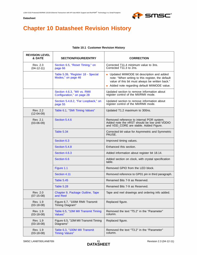
SMSC LAN8700/LAN8700i Revision 2.3 (04-12-11) DATASHEET Datasheet PRODUCT FEATURES LAN8700/LAN8700i ±15kV ESD Protected MII/RMII 10/100 Ethernet Transceiver with HP Auto-MDIX Support and flexPWR ® Technology in a Small Footprint Single-Chip Ethernet Physical Layer Transceiver (PHY) ESD Protection levels of ±8kV HBM without external protection devices ESD protection levels of EN/IEC61000-4-2, ±8kV contact mode, and ±15kV for air discharge mode per independent test facility Comprehensive flexPWR ® Technology — Flexible Power Management Architecture LVCMOS Variable I/O voltage range: +1.6V to +3.6V Integrated 3.3V to 1.8V regulator for optional single supply operation. — Regulator can be disabled if 1.8V system supply is available. Performs HP Auto-MDIX in accordance with IEEE 802.3ab specification Cable length greater than 150 meters Automatic Polarity Correction Latch-Up Performance Exceeds 150mA per EIA/JESD 78, Class II Energy Detect power-down mode Low Current consumption power down mode Low operating current consumption: — 39mA typical in 10BASE-T and — 79mA typical in 100BASE-TX mode Supports Auto-negotiation and Parallel Detection Supports the Media Independent Interface (MII) and Reduced Media Independent Interface (RMII) Compliant with IEEE 802.3-2005 standards — MII Pins tolerant to 3.6V IEEE 802.3-2005 compliant register functions Integrated DSP with Adaptive Equalizer Baseline Wander (BLW) Correction Vendor Specific register functions Low profile 36-pin QFN lead-free RoHS compliant package (6 x 6 x 0.9mm height) 4 LED status indicators Commercial Operating Temperature 0° C to 70° C Industrial Operating Temperature -40° C to 85° C version available (LAN8700i) Applications Set Top Boxes Network Printers and Servers LAN on Motherboard 10/100 PCMCIA/CardBus Applications Embedded Telecom Applications Video Record/Playback Systems Cable Modems/Routers DSL Modems/Routers Digital Video Recorders Personal Video Recorders IP and Video Phones Wireless Access Points Digital Televisions Digital Media Adaptors/Servers POS Terminals Automotive Networking Gaming Consoles Security Systems POE Applications Access Control
Transcript
SMSC LAN8700/LAN8700iDATASHE
PRODUCT FEATURES
LAN8700/LAN8700i
±15kV ESD Protected MII/RMII 10/100 Ethernet Transceiver with HP Auto-MDIX Support and flexPWR® Technology in a Small Footprint
Datasheet
Single-Chip Ethernet Physical Layer Transceiver (PHY)ESD Protection levels of ±8kV HBM without external protection devicesESD protection levels of EN/IEC61000-4-2, ±8kV contact mode, and ±15kV for air discharge mode per independent test facilityComprehensive flexPWR® Technology — Flexible Power Management ArchitectureLVCMOS Variable I/O voltage range: +1.6V to +3.6VIntegrated 3.3V to 1.8V regulator for optional single supply operation.— Regulator can be disabled if 1.8V system supply is
available.Performs HP Auto-MDIX in accordance with IEEE 802.3ab specificationCable length greater than 150 metersAutomatic Polarity CorrectionLatch-Up Performance Exceeds 150mA per EIA/JESD 78, Class IIEnergy Detect power-down modeLow Current consumption power down modeLow operating current consumption: — 39mA typical in 10BASE-T and — 79mA typical in 100BASE-TX modeSupports Auto-negotiation and Parallel DetectionSupports the Media Independent Interface (MII) and Reduced Media Independent Interface (RMII)Compliant with IEEE 802.3-2005 standards— MII Pins tolerant to 3.6VIEEE 802.3-2005 compliant register functionsIntegrated DSP with Adaptive EqualizerBaseline Wander (BLW) CorrectionVendor Specific register functionsLow profile 36-pin QFN lead-free RoHS compliant package (6 x 6 x 0.9mm height)4 LED status indicatorsCommercial Operating Temperature 0° C to 70° CIndustrial Operating Temperature -40° C to 85° C version available (LAN8700i)
ApplicationsSet Top BoxesNetwork Printers and ServersLAN on Motherboard10/100 PCMCIA/CardBus ApplicationsEmbedded Telecom ApplicationsVideo Record/Playback SystemsCable Modems/RoutersDSL Modems/RoutersDigital Video RecordersPersonal Video RecordersIP and Video PhonesWireless Access PointsDigital TelevisionsDigital Media Adaptors/ServersPOS TerminalsAutomotive NetworkingGaming ConsolesSecurity SystemsPOE ApplicationsAccess Control
Revision 2.3 (04-12-11)ET
±15kV ESD Protected MII/RMII 10/100 Ethernet Transceiver with HP Auto-MDIX Support and flexPWR® Technology in a Small Footprint
Datasheet
Order Numbers:
LAN8700C-AEZG for 36-pin, QFN lead-free RoHS compliant package
LAN8700iC-AEZG for (Industrial Temp) 36-pin, QFN lead-free RoHS compliant package
4900 pcs per tray
LAN8700C-AEZG-TR for 36-pin, QFN lead-free RoHS compliant package (tape and reel)
3000 pcs per reel
This product meets the halogen maximum concentration values per IEC61249-2-21
For RoHS compliance and environmental information, please visit www.smsc.com/rohs
80 ARKAY DRIVE, HAUPPAUGE, NY 11788 (631) 435-6000 or 1 (800) 443-SEMI
Circuit diagrams and other information relating to SMSC products are included as a means of illustrating typical applications. Consequently, complete information sufficient forconstruction purposes is not necessarily given. Although the information has been checked and is believed to be accurate, no responsibility is assumed for inaccuracies. SMSCreserves the right to make changes to specifications and product descriptions at any time without notice. Contact your local SMSC sales office to obtain the latest specificationsbefore placing your product order. The provision of this information does not convey to the purchaser of the described semiconductor devices any licenses under any patentrights or other intellectual property rights of SMSC or others. All sales are expressly conditional on your agreement to the terms and conditions of the most recently datedversion of SMSC's standard Terms of Sale Agreement dated before the date of your order (the "Terms of Sale Agreement"). The product may contain design defects or errorsknown as anomalies which may cause the product's functions to deviate from published specifications. Anomaly sheets are available upon request. SMSC products are notdesigned, intended, authorized or warranted for use in any life support or other application where product failure could cause or contribute to personal injury or severe propertydamage. Any and all such uses without prior written approval of an Officer of SMSC and further testing and/or modification will be fully at the risk of the customer. Copies ofthis document or other SMSC literature, as well as the Terms of Sale Agreement, may be obtained by visiting SMSC’s website at http://www.smsc.com. SMSC is a registeredtrademark of Standard Microsystems Corporation (“SMSC”). Product names and company names are the trademarks of their respective holders.
SMSC DISCLAIMS AND EXCLUDES ANY AND ALL WARRANTIES, INCLUDING WITHOUT LIMITATION ANY AND ALL IMPLIED WARRANTIES OF MERCHANTABILITY,FITNESS FOR A PARTICULAR PURPOSE, TITLE, AND AGAINST INFRINGEMENT AND THE LIKE, AND ANY AND ALL WARRANTIES ARISING FROM ANY COURSEOF DEALING OR USAGE OF TRADE. IN NO EVENT SHALL SMSC BE LIABLE FOR ANY DIRECT, INCIDENTAL, INDIRECT, SPECIAL, PUNITIVE, OR CONSEQUENTIALDAMAGES; OR FOR LOST DATA, PROFITS, SAVINGS OR REVENUES OF ANY KIND; REGARDLESS OF THE FORM OF ACTION, WHETHER BASED ON CONTRACT;TORT; NEGLIGENCE OF SMSC OR OTHERS; STRICT LIABILITY; BREACH OF WARRANTY; OR OTHERWISE; WHETHER OR NOT ANY REMEDY OF BUYER IS HELDTO HAVE FAILED OF ITS ESSENTIAL PURPOSE, AND WHETHER OR NOT SMSC HAS BEEN ADVISED OF THE POSSIBILITY OF SUCH DAMAGES.
±15kV ESD Protected MII/RMII 10/100 Ethernet Transceiver with HP Auto-MDIX Support and flexPWR® Technology in a Small Footprint
Datasheet
Chapter 1 General Description
The SMSC LAN8700/LAN8700i is a low-power, industrial temperature (LAN8700i), variable I/O voltage,analog interface IC with HP Auto-MDIX support for high-performance embedded Ethernet applications.The LAN8700/LAN8700i can be configured to operate on a single 3.3V supply utilizing an integrated3.3V to 1.8V linear regulator. An option is available to disable the linear regulator to optimize systemdesigns that have a 1.8V power plane available.
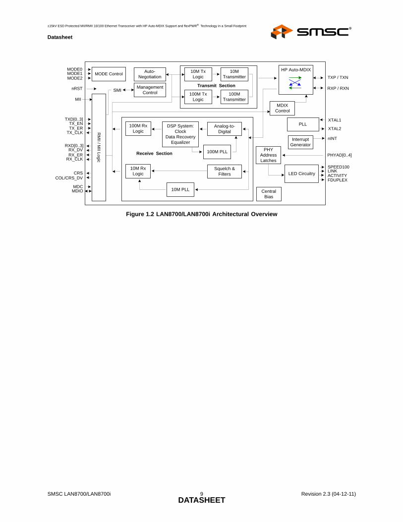
1.1 Architectural OverviewThe LAN8700/LAN8700i consists of an encoder/decoder, scrambler/descrambler, wave-shapingtransmitter, output driver, twisted-pair receiver with adaptive equalizer and baseline wander (BLW)correction, and clock and data recovery functions. The LAN8700/LAN8700i can be configured tosupport either the Media Independent Interface (MII) or the Reduced Media Independent Interface(RMII).
The LAN8700/LAN8700i is compliant with IEEE 802.3-2005 standards (MII Pins tolerant to 3.6V) andsupports both IEEE 802.3-2005 compliant and vendor-specific register functions. It contains a full-duplex 10-BASE-T/100BASE-TX transceiver and supports 10-Mbps (10BASE-T) operation onCategory 3 and Category 5 unshielded twisted-pair cable, and 100-Mbps (100BASE-TX) operation onCategory 5 unshielded twisted-pair cable.
Hubs and switches with multiple integrated MACs and external PHYs can have a large pin count dueto the high number of pins needed for each MII interface. An increasing pin count causes increasingcost.
The RMII interface is intended for use on Switch based ASICs or other embedded solutions requiringminimal pincount for ethernet connectivity. RMII requires only 6 pins for each MAC to PHY interfaceplus one common reference clock. The MII requires 16 pins for each MAC to PHY interface.
The SMSC LAN8700/LAN8700i is capable of running in RMII mode. Please contact your SMSC salesrepresentative for the latest RMII specification.
The LAN8700/LAN8700i referenced throughout this document applies to both the commercialtemperature and industrial temperature components. The LAN8700i refers to only the industrialtemperature component.
Figure 1.1 LAN8700/LAN8700i System Block Diagram
10/100MediaAccess
Controller(MAC)or SOC
SMSCLAN8700/LAN8700i
Magnetics Ethernet
System Bus
LEDS/GPIO
25 MHz (MII) or 50MHz (RMIII)Crystal or External Clock
±15kV ESD Protected MII/RMII 10/100 Ethernet Transceiver with HP Auto-MDIX Support and flexPWR® Technology in a Small Footprint
Datasheet
Chapter 3 Pin Description
This chapter describes the signals on each pin. When a lower case “n” is used at the beginning of thesignal name, it indicates that the signal is active low. For example, nRST indicates that the reset signalis active low.
3.1 I/O Signals
The following buffer types are shown in the TYPE column of the tables in this chapter.
I Input. Digital LVCMOS levels.
IPD Input with internal pull-down. Digital LVCMOS levels.
O Output. Digital LVCMOS levels.
OPD Output with internal pull-down. Digital LVCMOS levels.
I/O Input or Output . Digital LVCMOS levels.
IOPD Input or Output with internal pull-down. Digital LVCMOS levels.
IOPU Input or Output with internal pull-up. Digital LVCMOS levels.
Note: The digital signals are not 5V tolerant.They are variable voltage from +1.6V to +3.6V.
AI Input. Analog levels..
AO Output. Analog levels.
Table 3.1 MII Signals
SIGNAL NAME TYPE DESCRIPTION
TXD0 I Transmit Data 0: Bit 0 of the 4 data bits that are accepted by the PHY for transmission.
TXD1 I Transmit Data 1: Bit 1 of the 4 data bits that are accepted by the PHY for transmission.
TXD2 I Transmit Data 2: Bit 2 of the 4 data bits that are accepted by the PHY for transmissionNote: This signal should be grounded in RMII Mode.
TXD3 I Transmit Data 3: Bit 3 of the 4 data bits that are accepted by the PHY for transmission. Note: This signal should be grounded in RMII Mode
nINT/TX_ER/TXD4
IOPU MII Transmit Error: When driven high, the 4B/5B encode process substitutes the Transmit Error code-group (/H/) for the encoded data word. This input is ignored in 10Base-T operation.
MII Transmit Data 4: In Symbol Interface (5B Decoding) mode, this signal becomes the MII Transmit Data 4 line, the MSB of the 5-bit symbol code-group.
Notes:This signal is not used in RMII Mode.This signal is mux’d with nINTSee Section 4.10, "nINT/TX_ER/TXD4 Strapping," on page 32 for additional information on configuration/strapping options.
TX_EN IPD Transmit Enable: Indicates that valid data is presented on the TXD[3:0] signals, for transmission. In RMII Mode, only TXD[1:0] have valid data.
±15kV ESD Protected MII/RMII 10/100 Ethernet Transceiver with HP Auto-MDIX Support and flexPWR® Technology in a Small Footprint
Datasheet
TX_CLK O Transmit Clock: 25MHz in 100Base-TX mode. 2.5MHz in 10Base-T mode.Note: This signal is not used in RMII Mode.
Note: For proper TXCLK operation, RX_ER and RX_DV must NOT be driven high externally on a hardware reset or on a LAN8700 power up.
RXD0/MODE0
IOPU Receive Data 0: Bit 0 of the 4 data bits that are sent by the PHY in the receive path.
PHY Operating Mode Bit 0: set the default MODE of the PHY. Note: See Section 5.4.9.2, "Mode Bus – MODE[2:0]," on
page 56, for the MODE options
RXD1/MODE1
IOPU Receive Data 1: Bit 1 of the 4 data bits that are sent by the PHY in the receive path.
PHY Operating Mode Bit 1: set the default MODE of the PHY. Note: See Section 5.4.9.2, "Mode Bus – MODE[2:0]," on
page 56, for the MODE options.
RXD2/MODE2
IOPU Receive Data 2: Bit 2 of the 4 data bits that are sent by the PHY in the receive path.
PHY Operating Mode Bit 2: set the default MODE of the PHY.
Notes:RXD2 is not used in RMII Mode.See Section 5.4.9.2, "Mode Bus – MODE[2:0]," on page 56, for the MODE options.
RXD3/nINTSEL
IOPU Receive Data 3: Bit 3 of the 4 data bits that are sent by the PHY in the receive path.
nINTSEL: On power-up or external reset, the mode of the nINT/TXER/TXD4 pin is selected.
When RXD3/nINTSEL is floated or pulled to VDDIO, nINT is selected for operation on pin nINT/TXER/TXD4 (default).When RXD3/nINTSEL is pulled low to VSS through a resistor, (see Table 4.3, “Boot Strapping Configuration Resistors,” on page 33), TXER/TXD4 is selected for operation on pin nINT/TXER/TXD4.
Notes:RXD3 is not used in RMII ModeIf the nINT/TXER/TXD4 pin is configured for nINT mode, then a pull-up resistor is needed to VDDIO on the nINT/TXER/TXD4 pin. see Table 4.3, “Boot Strapping Configuration Resistors,” on page 33.See Section 4.10, "nINT/TX_ER/TXD4 Strapping," on page 32 for additional information on configuration/strapping options.
±15kV ESD Protected MII/RMII 10/100 Ethernet Transceiver with HP Auto-MDIX Support and flexPWR® Technology in a Small Footprint
Datasheet
RX_ER/RXD4/
OPD Receive Error: Asserted to indicate that an error was detected somewhere in the frame presently being transferred from the PHY.
MII Receive Data 4: In Symbol Interface (5B Decoding) mode, this signal is the MII Receive Data 4 signal, the MSB of the received 5-bit symbol code-group. Unless configured in this mode, the pin functions as RX_ER.Note: This pin has an internal pull-down resistor, and must not
be high during reset. The RX_ER signal is optional in RMII Mode.
RX_DV O Receive Data Valid: Indicates that recovered and decoded data nibbles are being presented on RXD[3:0]. Note: This pin has an internal pull-down resistor, and must not
be high during reset. This signal is not used in RMII Mode.
RX_CLK/REGOFF
IOPD Receive Clock: In MII mode, this pin is the receive clock output. 25MHz in 100Base-TX mode. 2.5MHz in 10Base-T mode.Note: This signal is not used in RMII Mode.Regulator Off: This pin pulled up to configure the internal 1.8V regulator off. As described in Section 4.9, this pin is sampled during the power-on sequence to determine if the internal regulator should turn on. When the regulator is disabled, external 1.8V must be supplied to VDD_CORE, and the voltage at VDD33 must be at least 2.64V before voltage is applied to VDD_CORE.
COL/RMII/
CRS_DV
IOPD MII Mode Collision Detect: Asserted to indicate detection of collision condition.
RMII – MII/RMII mode selection is latched on the rising edge of the internal reset (nreset) based on the following strapping:
Float this pin for MII mode or pull-high with an external resistor to VDDIO (see Table 4.3, “Boot Strapping Configuration Resistors,” on page 33) to set the device in RMII mode.See Section 4.6.3, "MII vs. RMII Configuration," on page 28 for more details.
RMII Mode CRS_DV (Carrier Sense/Receive Data Valid) Asserted to indicate when the receive medium is non-idle. When a 10BT packet is received, CRS_DV is asserted, but RXD[1:0] is held low until the SFD byte (10101011) is received. In 10BT, half-duplex mode, transmitted data is not looped back onto the receive data pins, per the RMII standard.
CRS/PHYAD4
IOPU Carrier Sense: Indicates detection of carrier. Note: This signal is mux’d with PHYAD4
±15kV ESD Protected MII/RMII 10/100 Ethernet Transceiver with HP Auto-MDIX Support and flexPWR® Technology in a Small Footprint
Datasheet
Table 3.2 LED Signals
SIGNAL NAME TYPE DESCRIPTION
SPEED100/PHYAD0
IOPU LED1 – SPEED100 indication. Active indicates that the selected speed is 100Mbps. Inactive indicates that the selected speed is 10Mbps.Note: This signal is mux’d with PHYAD0
LINK/PHYAD1
IOPU LED2 – LINK ON indication. Active indicates that the Link (100Base-TX or 10Base-T) is on.Note: This signal is mux’d with PHYAD1
ACTIVITY/PHYAD2
IOPU LED3 – ACTIVITY indication. Active indicates that there is Carrier sense (CRS) from the active PMD. Note: This signal is mux’d with PHYAD2
FDUPLEX/PHYAD3
IOPU LED4 – DUPLEX indication. Active indicates that the PHY is in full-duplex mode.Note: This signal is mux’d with PHYAD3
Table 3.3 Management Signals
SIGNAL NAME TYPE DESCRIPTION
MDIO IOPD Management Data Input/OUTPUT: Serial management data input/output.
MDC IPD Management Clock: Serial management clock.
IOPU PHY Address Bit 4: set the default address of the PHY. This signal is mux’d with CRSNote: This signal is mux’d with CRS
FDUPLEX/PHYAD3
IOPU PHY Address Bit 3: set the default address of the PHY.Note: This signal is mux’d with FDUPLEX
ACTIVITY/PHYAD2
IOPU PHY Address Bit 2: set the default address of the PHY.Note: This signal is mux’d with ACTIVITY
LINK/PHYAD1
IOPU PHY Address Bit 1: set the default address of the PHY.Note: This signal is mux’d with LINK
SPEED100/PHYAD0
IOPU PHY Address Bit 0: set the default address of the PHY.Note: This signal is mux’d with SPEED100
RXD2/MODE2
IOPU PHY Operating Mode Bit 2: set the default MODE of the PHY. See Section 5.4.9.2, "Mode Bus – MODE[2:0]," on page 56, for the MODE options.Note: This signal is mux’d with RXD2
±15kV ESD Protected MII/RMII 10/100 Ethernet Transceiver with HP Auto-MDIX Support and flexPWR® Technology in a Small Footprint
Datasheet
Note 3.1 On nRST transition high, the PHY latches the state of the configuration pins in this table.
RXD1/MODE1
IOPU PHY Operating Mode Bit 1: set the default MODE of the PHY. See Section 5.4.9.2, "Mode Bus – MODE[2:0]," on page 56, for the MODE options.Note: This signal is mux’d with RXD1
RXD0/MODE0
IOPU PHY Operating Mode Bit 0: set the default MODE of the PHY. See Section 5.4.9.2, "Mode Bus – MODE[2:0]," on page 56, for the MODE options.Note: This signal is mux’d with RXD0
COL/RMII/
CRS_DV
IOPD Digital Communication Mode: set the digital communications mode of the PHY to RMII or MII. This signal is muxed with the Collision signal (MII mode) and Carrier Sense/ receive Data Valid (RMII mode)
Float for MII mode. Pull up with a resistor to VDDIO for RMII mode (see Table 4.3, “Boot Strapping Configuration Resistors,” on page 33) .
RXD3/nINTSEL
IOPU nINT pin mode select: set the mode of pin 1.Default, left floating pin 1 is nINT, active low interrupt output.
Notes:For nINT mode, tie nINT/TXD4/TXER to VDDIO with a resistor (see Table 4.3, “Boot Strapping Configuration Resistors,” on page 33).
Pulled to VSS by a resistor, (see Table 4.3, “Boot Strapping Configuration Resistors,” on page 33) pin 1 is TX_ER/TXD4, Transmit Error or Transmit data 4 (5B mode).
Notes:For TXD4/TXER mode, do not tie nINT/TXD4/TXER to VDDIO or Ground.
Table 3.5 General Signals
SIGNAL NAME TYPE DESCRIPTION
nINT/TX_ER/TXD4
IOPU LAN Interrupt – Active Low output. Place an external resistor (see Table 4.3, “Boot Strapping Configuration Resistors,” on page 33) pull-up to VCC 3.3V.
Notes:This signal is mux’d with TXER/TXD4See Section 4.10, "nINT/TX_ER/TXD4 Strapping," on page 32 for additional details on Strapping options.
nRST I External Reset – input of the system reset. This signal is active LOW. When this pin is deasserted, the mode register bits are loaded from the mode pins as described in Section 5.4.9.2.
±15kV ESD Protected MII/RMII 10/100 Ethernet Transceiver with HP Auto-MDIX Support and flexPWR® Technology in a Small Footprint
Datasheet
CLKIN/XTAL1
I/O Clock Input – 25 Mhz or 50 MHz external clock or crystal input.
In MII mode, this signal is the 25 MHz reference input clock
In RMII mode, this signal is the 50 MHz reference input clock which is typically also driven to the RMII compliant Ethernet MAC clock input.Note: See Section 4.10, "nINT/TX_ER/TXD4 Strapping," on
page 32 for additional details on Strapping options.
XTAL2 O Clock Output – 25 MHz crystal output.Note: Float this pin if using an external clock being driven
through CLKIN/XTAL1
Table 3.6 10/100 Line Interface
SIGNAL NAME TYPE DESCRIPTION
TXP AO Transmit Data Positive: 100Base-TX or 10Base-T differential transmit outputs to magnetics.
TXN AO Transmit Data Negative: 100Base-TX or 10Base-T differential transmit outputs to magnetics.
RXP AI Receive Data Positive: 100Base-TX or 10Base-T differential receive inputs from magnetics.
RXN AI Receive Data Negative: 100Base-TX or 10Base-T differential receive inputs from magnetics.
Table 3.7 Analog References
SIGNAL NAME TYPE DESCRIPTION
EXRES1 AI Connects to reference resistor of value 12.4K-Ohm, 1% connected as described in the Analog Layout Guidelines. The nominal voltage is 1.2V and therefore the resistor will dissipate approximately 1mW of power.
±15kV ESD Protected MII/RMII 10/100 Ethernet Transceiver with HP Auto-MDIX Support and flexPWR® Technology in a Small Footprint
Datasheet
VDD_CORE POWER +1.8V (Core voltage) - 1.8V for digital circuitry on chip. Supplied by the on-chip regulator unless configured for regulator off mode using the RX_CLK/REGOFF pin. Place a 0.1uF capacitor near this pin and connect the capacitor from this pin to ground. When using the on-chip regulator, place a 4.7uF ±20% capacitor with ESR < 1ohm near this pin and connect the capacitor from this pin to ground. X5R or X7R ceramic capacitors are recommended since they exhibit an ESR lower than 0.1ohm at frequencies greater than 10kHz.
VSS POWER
Exposed Ground Flag. The flag must be connected to the ground plane with an array of vias as described in the Analog Layout Guidelines
±15kV ESD Protected MII/RMII 10/100 Ethernet Transceiver with HP Auto-MDIX Support and flexPWR® Technology in a Small Footprint
Datasheet
Chapter 4 Architecture Details
4.1 Top Level Functional ArchitectureFunctionally, the PHY can be divided into the following sections:
100Base-TX transmit and receive
10Base-T transmit and receive
MII or RMII interface to the controller
Auto-negotiation to automatically determine the best speed and duplex possible
Management Control to read status registers and write control registers
Figure 4.1 100Base-TX Data Path
4.2 100Base-TX TransmitThe data path of the 100Base-TX is shown in Figure 4.1. Each major block is explained below.
4.2.1 100M Transmit Data Across the MII/RMII Interface
For MII, the MAC controller drives the transmit data onto the TXD bus and asserts TX_EN to indicatevalid data. The data is latched by the PHY’s MII block on the rising edge of TX_CLK. The data is inthe form of 4-bit wide 25MHz data.
The MAC controller drives the transmit data onto the TXD bus and asserts TX_EN to indicate validdata. The data is latched by the PHY’s MII block on the rising edge of REF_CLK. The data is in theform of 2-bit wide 50MHz data.
4.2.2 4B/5B Encoding
The transmit data passes from the MII block to the 4B/5B encoder. This block encodes the data from4-bit nibbles to 5-bit symbols (known as “code-groups”) according to Table 4.1. Each 4-bit data-nibbleis mapped to 16 of the 32 possible code-groups. The remaining 16 code-groups are either used forcontrol information or are not valid.
±15kV ESD Protected MII/RMII 10/100 Ethernet Transceiver with HP Auto-MDIX Support and flexPWR® Technology in a Small Footprint
Datasheet
The first 16 code-groups are referred to by the hexadecimal values of their corresponding data nibbles,0 through F. The remaining code-groups are given letter designations with slashes on either side. Forexample, an IDLE code-group is /I/, a transmit error code-group is /H/, etc.
The encoding process may be bypassed by clearing bit 6 of register 31. When the encoding isbypassed the 5th transmit data bit is equivalent to TX_ER.
Note that encoding can be bypassed only when the MAC interface is configured to operate in MIImode.
Table 4.1 4B/5B Code Table
CODEGROUP SYM
RECEIVERINTERPRETATION
TRANSMITTERINTERPRETATION
11110 0 0 0000 DATA 0 0000 DATA
01001 1 1 0001 1 0001
10100 2 2 0010 2 0010
10101 3 3 0011 3 0011
01010 4 4 0100 4 0100
01011 5 5 0101 5 0101
01110 6 6 0110 6 0110
01111 7 7 0111 7 0111
10010 8 8 1000 8 1000
10011 9 9 1001 9 1001
10110 A A 1010 A 1010
10111 B B 1011 B 1011
11010 C C 1100 C 1100
11011 D D 1101 D 1101
11100 E E 1110 E 1110
11101 F F 1111 F 1111
11111 I IDLE Sent after /T/R until TX_EN
11000 J First nibble of SSD, translated to “0101” following IDLE, else RX_ER
Sent for rising TX_EN
10001 K Second nibble of SSD, translated to “0101” following J, else RX_ER
Sent for rising TX_EN
01101 T First nibble of ESD, causes de-assertion of CRS if followed by /R/, else assertion of RX_ER
Sent for falling TX_EN
00111 R Second nibble of ESD, causes deassertion of CRS if following /T/, else assertion of RX_ER
Sent for falling TX_EN
00100 H Transmit Error Symbol Sent for rising TX_ER
±15kV ESD Protected MII/RMII 10/100 Ethernet Transceiver with HP Auto-MDIX Support and flexPWR® Technology in a Small Footprint
Datasheet
4.2.3 Scrambling
Repeated data patterns (especially the IDLE code-group) can have power spectral densities with largenarrow-band peaks. Scrambling the data helps eliminate these peaks and spread the signal powermore uniformly over the entire channel bandwidth. This uniform spectral density is required by FCCregulations to prevent excessive EMI from being radiated by the physical wiring.
The seed for the scrambler is generated from the PHY address, PHYAD[4:0], ensuring that in multiple-PHY applications, such as repeaters or switches, each PHY will have its own scrambler sequence.
The scrambler also performs the Parallel In Serial Out conversion (PISO) of the data.
4.2.4 NRZI and MLT3 Encoding
The scrambler block passes the 5-bit wide parallel data to the NRZI converter where it becomes aserial 125MHz NRZI data stream. The NRZI is encoded to MLT-3. MLT3 is a tri-level code where achange in the logic level represents a code bit “1” and the logic output remaining at the same levelrepresents a code bit “0”.
4.2.5 100M Transmit Driver
The MLT3 data is then passed to the analog transmitter, which drives the differential MLT-3 signal, onoutputs TXP and TXN, to the twisted pair media across a 1:1 ratio isolation transformer. The 10Base-T and 100Base-TX signals pass through the same transformer so that common “magnetics” can beused for both. The transmitter drives into the 100Ω impedance of the CAT-5 cable. Cable terminationand impedance matching require external components.
±15kV ESD Protected MII/RMII 10/100 Ethernet Transceiver with HP Auto-MDIX Support and flexPWR® Technology in a Small Footprint
Datasheet
4.2.6 100M Phase Lock Loop (PLL)
The 100M PLL locks onto reference clock and generates the 125MHz clock used to drive the 125 MHzlogic and the 100Base-Tx Transmitter.
Figure 4.2 Receive Data Path
4.3 100Base-TX ReceiveThe receive data path is shown in Figure 4.2. Detailed descriptions are given below.
4.3.1 100M Receive Input
The MLT-3 from the cable is fed into the PHY (on inputs RXP and RXN) via a 1:1 ratio transformer.The ADC samples the incoming differential signal at a rate of 125M samples per second. Using a 64-level quanitizer it generates 6 digital bits to represent each sample. The DSP adjusts the gain of theADC according to the observed signal levels such that the full dynamic range of the ADC can be used.
4.3.2 Equalizer, Baseline Wander Correction and Clock and Data Recovery
The 6 bits from the ADC are fed into the DSP block. The equalizer in the DSP section compensatesfor phase and amplitude distortion caused by the physical channel consisting of magnetics, connectors,and CAT- 5 cable. The equalizer can restore the signal for any good-quality CAT-5 cable between 1mand 150m.
If the DC content of the signal is such that the low-frequency components fall below the low frequencypole of the isolation transformer, then the droop characteristics of the transformer will becomesignificant and Baseline Wander (BLW) on the received signal will result. To prevent corruption of thereceived data, the PHY corrects for BLW and can receive the ANSI X3.263-1995 FDDI TP-PMDdefined “killer packet” with no bit errors.
The 100M PLL generates multiple phases of the 125MHz clock. A multiplexer, controlled by the timingunit of the DSP, selects the optimum phase for sampling the data. This is used as the receivedrecovered clock. This clock is used to extract the serial data from the received signal.
MAC
A/D Converter
MLT-3 Converter
NRZI Converter
4B/5B Decoder
Magnetics CAT-5RJ45
100M PLL
MII 25Mhz by 4 bitsor
RMII 50Mhz by 2 bits
RX_CLK(for MII only)
25MHz by5 bits
NRZI
MLT-3MLT-3 MLT-3
6 bit Data
Descrambler and SIPO
125 Mbps Serial
DSP: Timing recovery, Equalizer and BLW Correction
±15kV ESD Protected MII/RMII 10/100 Ethernet Transceiver with HP Auto-MDIX Support and flexPWR® Technology in a Small Footprint
Datasheet
4.3.3 NRZI and MLT-3 Decoding
The DSP generates the MLT-3 recovered levels that are fed to the MLT-3 converter. The MLT-3 is thenconverted to an NRZI data stream.
4.3.4 Descrambling
The descrambler performs an inverse function to the scrambler in the transmitter and also performsthe Serial In Parallel Out (SIPO) conversion of the data.
During reception of IDLE (/I/) symbols. the descrambler synchronizes its descrambler key to theincoming stream. Once synchronization is achieved, the descrambler locks on this key and is able todescramble incoming data.
Special logic in the descrambler ensures synchronization with the remote PHY by searching for IDLEsymbols within a window of 4000 bytes (40us). This window ensures that a maximum packet size of1514 bytes, allowed by the IEEE 802.3 standard, can be received with no interference. If no IDLE-symbols are detected within this time-period, receive operation is aborted and the descrambler re-startsthe synchronization process.
The descrambler can be bypassed by setting bit 0 of register 31.
4.3.5 Alignment
The de-scrambled signal is then aligned into 5-bit code-groups by recognizing the /J/K/ Start-of-StreamDelimiter (SSD) pair at the start of a packet. Once the code-word alignment is determined, it is storedand utilized until the next start of frame.
4.3.6 5B/4B Decoding
The 5-bit code-groups are translated into 4-bit data nibbles according to the 4B/5B table. Thetranslated data is presented on the RXD[3:0] signal lines. The SSD, /J/K/, is translated to “0101 0101”as the first 2 nibbles of the MAC preamble. Reception of the SSD causes the PHY to assert the RX_DVsignal, indicating that valid data is available on the RXD bus. Successive valid code-groups aretranslated to data nibbles. Reception of either the End of Stream Delimiter (ESD) consisting of the /T/R/symbols, or at least two /I/ symbols causes the PHY to de-assert carrier sense and RX_DV.
These symbols are not translated into data.
The decoding process may be bypassed by clearing bit 6 of register 31. When the decoding isbypassed the 5th receive data bit is driven out on RX_ER/RXD4. Decoding may be bypassed onlywhen the MAC interface is in MII mode.
4.3.7 Receive Data Valid Signal
The Receive Data Valid signal (RX_DV) indicates that recovered and decoded nibbles are beingpresented on the RXD[3:0] outputs synchronous to RX_CLK. RX_DV becomes active after the /J/K/delimiter has been recognized and RXD is aligned to nibble boundaries. It remains active until eitherthe /T/R/ delimiter is recognized or link test indicates failure or SIGDET becomes false.
RX_DV is asserted when the first nibble of translated /J/K/ is ready for transfer over the MediaIndependent Interface (MII mode).
±15kV ESD Protected MII/RMII 10/100 Ethernet Transceiver with HP Auto-MDIX Support and flexPWR® Technology in a Small Footprint
Datasheet
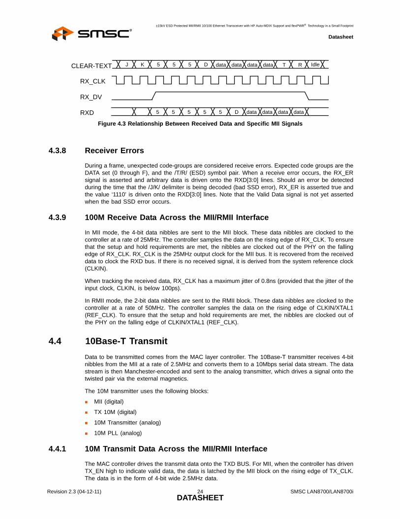
Figure 4.3 Relationship Between Received Data and Specific MII Signals
4.3.8 Receiver Errors
During a frame, unexpected code-groups are considered receive errors. Expected code groups are theDATA set (0 through F), and the /T/R/ (ESD) symbol pair. When a receive error occurs, the RX_ERsignal is asserted and arbitrary data is driven onto the RXD[3:0] lines. Should an error be detectedduring the time that the /J/K/ delimiter is being decoded (bad SSD error), RX_ER is asserted true andthe value ‘1110’ is driven onto the RXD[3:0] lines. Note that the Valid Data signal is not yet assertedwhen the bad SSD error occurs.
4.3.9 100M Receive Data Across the MII/RMII Interface
In MII mode, the 4-bit data nibbles are sent to the MII block. These data nibbles are clocked to thecontroller at a rate of 25MHz. The controller samples the data on the rising edge of RX_CLK. To ensurethat the setup and hold requirements are met, the nibbles are clocked out of the PHY on the fallingedge of RX_CLK. RX_CLK is the 25MHz output clock for the MII bus. It is recovered from the receiveddata to clock the RXD bus. If there is no received signal, it is derived from the system reference clock(CLKIN).
When tracking the received data, RX_CLK has a maximum jitter of 0.8ns (provided that the jitter of theinput clock, CLKIN, is below 100ps).
In RMII mode, the 2-bit data nibbles are sent to the RMII block. These data nibbles are clocked to thecontroller at a rate of 50MHz. The controller samples the data on the rising edge of CLKIN/XTAL1(REF_CLK). To ensure that the setup and hold requirements are met, the nibbles are clocked out ofthe PHY on the falling edge of CLKIN/XTAL1 (REF_CLK).
4.4 10Base-T TransmitData to be transmitted comes from the MAC layer controller. The 10Base-T transmitter receives 4-bitnibbles from the MII at a rate of 2.5MHz and converts them to a 10Mbps serial data stream. The datastream is then Manchester-encoded and sent to the analog transmitter, which drives a signal onto thetwisted pair via the external magnetics.
The 10M transmitter uses the following blocks:
MII (digital)
TX 10M (digital)
10M Transmitter (analog)
10M PLL (analog)
4.4.1 10M Transmit Data Across the MII/RMII Interface
The MAC controller drives the transmit data onto the TXD BUS. For MII, when the controller has drivenTX_EN high to indicate valid data, the data is latched by the MII block on the rising edge of TX_CLK.The data is in the form of 4-bit wide 2.5MHz data.
±15kV ESD Protected MII/RMII 10/100 Ethernet Transceiver with HP Auto-MDIX Support and flexPWR® Technology in a Small Footprint
Datasheet
In order to comply with legacy 10Base-T MAC/Controllers, in Half-duplex mode the PHY loops backthe transmitted data, on the receive path. This does not confuse the MAC/Controller since the COLsignal is not asserted during this time. The PHY also supports the SQE (Heartbeat) signal. See Section5.4.2, "Collision Detect," on page 51, for more details.
For RMII, TXD[1:0] shall transition synchronously with respect to REF_CLK. When TX_EN is asserted,TXD[1:0] are accepted for transmission by the LAN8700/LAN8700i. TXD[1:0] shall be “00” to indicateidle when TX_EN is deasserted. Values of TXD[1:0] other than “00” when TX_EN is deasserted arereserved for out-of-band signalling (to be defined). Values other than “00” on TXD[1:0] while TX_EN isdeasserted shall be ignored by the LAN8700/LAN8700i.TXD[1:0] shall provide valid data for eachREF_CLK period while TX_EN is asserted.
4.4.2 Manchester Encoding
The 4-bit wide data is sent to the TX10M block. The nibbles are converted to a 10Mbps serial NRZIdata stream. The 10M PLL locks onto the external clock or internal oscillator and produces a 20MHzclock. This is used to Manchester encode the NRZ data stream. When no data is being transmitted(TX_EN is low), the TX10M block outputs Normal Link Pulses (NLPs) to maintain communications withthe remote link partner.
4.4.3 10M Transmit Drivers
The Manchester encoded data is sent to the analog transmitter where it is shaped and filtered beforebeing driven out as a differential signal across the TXP and TXN outputs.
4.5 10Base-T ReceiveThe 10Base-T receiver gets the Manchester- encoded analog signal from the cable via the magnetics.It recovers the receive clock from the signal and uses this clock to recover the NRZI data stream. This10M serial data is converted to 4-bit data nibbles which are passed to the controller across the MII ata rate of 2.5MHz.
This 10M receiver uses the following blocks:
Filter and SQUELCH (analog)
10M PLL (analog)
RX 10M (digital)
MII (digital)
4.5.1 10M Receive Input and Squelch
The Manchester signal from the cable is fed into the PHY (on inputs RXP and RXN) via 1:1 ratiomagnetics. It is first filtered to reduce any out-of-band noise. It then passes through a SQUELCHcircuit. The SQUELCH is a set of amplitude and timing comparators that normally reject differentialvoltage levels below 300mV and detect and recognize differential voltages above 585mV.
4.5.2 Manchester Decoding
The output of the SQUELCH goes to the RX10M block where it is validated as Manchester encodeddata. The polarity of the signal is also checked. If the polarity is reversed (local RXP is connected toRXN of the remote partner and vice versa), then this is identified and corrected. The reversed conditionis indicated by the flag “XPOL“, bit 4 in register 27. The 10M PLL is locked onto the receivedManchester signal and from this, generates the received 20MHz clock. Using this clock, theManchester encoded data is extracted and converted to a 10MHz NRZI data stream. It is thenconverted from serial to 4-bit wide parallel data.
±15kV ESD Protected MII/RMII 10/100 Ethernet Transceiver with HP Auto-MDIX Support and flexPWR® Technology in a Small Footprint
Datasheet
The RX10M block also detects valid 10Base-T IDLE signals - Normal Link Pulses (NLPs) - to maintainthe link.
4.5.3 10M Receive Data Across the MII/RMII Interface
For MII, the 4 bit data nibbles are sent to the MII block. In MII mode, these data nibbles are valid onthe rising edge of the 2.5 MHz RX_CLK.
For RMII, the 2bit data nibbles are sent to the RMII block. In RMII mode, these data nibbles are validon the rising edge of the RMII REF_CLK.
4.5.4 Jabber Detection
Jabber is a condition in which a station transmits for a period of time longer than the maximumpermissible packet length, usually due to a fault condition, that results in holding the TX_EN input fora long period. Special logic is used to detect the jabber state and abort the transmission to the line,within 45ms. Once TX_EN is deasserted, the logic resets the jabber condition.
As shown in Table 5.31, bit 1.1 indicates that a jabber condition was detected.
4.6 MAC InterfaceThe MII/RMII block is responsible for the communication with the controller. Special sets of hand-shakesignals are used to indicate that valid received/transmitted data is present on the 4 bit receive/transmitbus.
The device must be configured in MII or RMII mode. See Section 4.6.3, "MII vs. RMII Configuration,"on page 28.
4.6.1 MII
The MII includes 16 interface signals:
transmit data - TXD[3:0]
transmit strobe - TX_EN
transmit clock - TX_CLK
transmit error - TX_ER/TXD4
receive data - RXD[3:0]
receive strobe - RX_DV
receive clock - RX_CLK
receive error - RX_ER/RXD4
collision indication - COL
carrier sense - CRS
In MII mode, on the transmit path, the PHY drives the transmit clock, TX_CLK, to the controller. Thecontroller synchronizes the transmit data to the rising edge of TX_CLK. The controller drives TX_ENhigh to indicate valid transmit data. The controller drives TX_ER high when a transmit error is detected.
On the receive path, the PHY drives both the receive data, RXD[3:0], and the RX_CLK signal. Thecontroller clocks in the receive data on the rising edge of RX_CLK when the PHY drives RX_DV high.The PHY drives RX_ER high when a receive error is detected.
±15kV ESD Protected MII/RMII 10/100 Ethernet Transceiver with HP Auto-MDIX Support and flexPWR® Technology in a Small Footprint
Datasheet
4.6.2 RMII
The SMSC LAN8700/LAN8700i supports the low pin count Reduced Media Independent Interface(RMII) intended for use between Ethernet PHYs and Switch ASICs. Under IEEE 802.3, an MIIcomprised of 16 pins for data and control is defined. In devices incorporating many MACs or PHYinterfaces such as switches, the number of pins can add significant cost as the port counts increase.The management interface (MDIO/MDC) is identical to MII. The RMII interface has the followingcharacteristics:
It is capable of supporting 10Mb/s and 100Mb/s data rates
A single clock reference is sourced from the MAC to PHY (or from an external source)
It provides independent 2 bit wide (di-bit) transmit and receive data paths
It uses LVCMOS signal levels, compatible with common digital CMOS ASIC processes
The RMII includes 6 interface signals with one of the signals being optional:
transmit data - TXD[1:0]
transmit strobe - TX_EN
receive data - RXD[1:0]
receive error - RX_ER (Optional)
carrier sense - CRS_DV
Reference Clock - CLKIN/XTAL1 (RMII references usually define this signal as REF_CLK)
4.6.2.1 Reference Clock
The Reference Clock - CLKIN, is a continuous clock that provides the timing reference for CRS_DV,RXD[1:0], TX_EN, TXD[1:0], and RX_ER. The Reference Clock is sourced by the MAC or an externalsource. Switch implementations may choose to provide REF_CLK as an input or an output dependingon whether they provide a REF_CLK output or rely on an external clock distribution device.
The “Reference Clock” frequency must be 50 MHz ± 50 ppm with a duty cycle between 40% and 60%inclusive. The SMSC LAN8700/LAN8700i uses the “Reference Clock” as the network clock such thatno buffering is required on the transmit data path. The SMSC LAN8700/LAN8700i will recover the clockfrom the incoming data stream, the receiver will account for differences between the local REF_CLKand the recovered clock through use of sufficient elasticity buffering. The elasticity buffer does notaffect the Inter-Packet Gap (IPG) for received IPGs of 36 bits or greater. To tolerate the clock variationsspecified here for Ethernet MTUs, the elasticity buffer shall tolerate a minimum of ±10 bits.
4.6.2.2 CRS_DV - Carrier Sense/Receive Data Valid
The CRS_DV is asserted by the LAN8700/LAN8700i when the receive medium is non-idle. CRS_DVis asserted asynchronously on detection of carrier due to the criteria relevant to the operating mode.That is, in 10BASE-T mode, when squelch is passed or in 100BASE-X mode when 2 non-contiguouszeroes in 10 bits are detected, carrier is said to be detected.
Loss of carrier shall result in the deassertion of CRS_DV synchronous to the cycle of REF_CLK whichpresents the first di-bit of a nibble onto RXD[1:0] (i.e. CRS_DV is deasserted only on nibbleboundaries). If the LAN8700/LAN8700i has additional bits to be presented on RXD[1:0] following theinitial deassertion of CRS_DV, then the LAN8700/LAN8700i shall assert CRS_DV on cycles ofREF_CLK which present the second di-bit of each nibble and de-assert CRS_DV on cycles ofREF_CLK which present the first di-bit of a nibble. The result is: Starting on nibble boundariesCRS_DV toggles at 25 MHz in 100Mb/s mode and 2.5 MHz in 10Mb/s mode when CRS ends beforeRX_DV (i.e. the FIFO still has bits to transfer when the carrier event ends.) Therefore, the MAC canaccurately recover RX_DV and CRS.
During a false carrier event, CRS_DV shall remain asserted for the duration of carrier activity. The dataon RXD[1:0] is considered valid once CRS_DV is asserted. However, since the assertion of CRS_DV
±15kV ESD Protected MII/RMII 10/100 Ethernet Transceiver with HP Auto-MDIX Support and flexPWR® Technology in a Small Footprint
Datasheet
is asynchronous relative to REF_CLK, the data on RXD[1:0] shall be “00” until proper receive signaldecoding takes place.
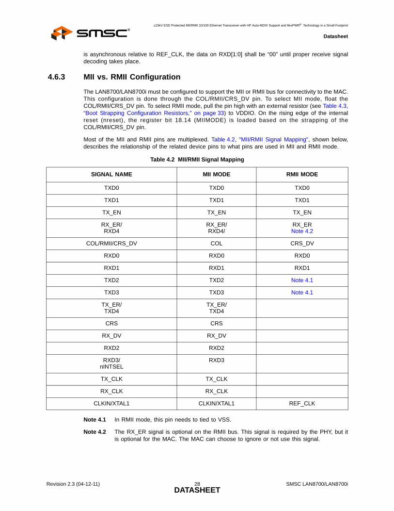
4.6.3 MII vs. RMII Configuration
The LAN8700/LAN8700i must be configured to support the MII or RMII bus for connectivity to the MAC.This configuration is done through the COL/RMII/CRS_DV pin. To select MII mode, float theCOL/RMII/CRS_DV pin. To select RMII mode, pull the pin high with an external resistor (see Table 4.3,“Boot Strapping Configuration Resistors,” on page 33) to VDDIO. On the rising edge of the internalreset (nreset), the register bit 18.14 (MIIMODE) is loaded based on the strapping of theCOL/RMII/CRS_DV pin.
Most of the MII and RMII pins are multiplexed. Table 4.2, "MII/RMII Signal Mapping", shown below,describes the relationship of the related device pins to what pins are used in MII and RMII mode.
Note 4.1 In RMII mode, this pin needs to tied to VSS.
Note 4.2 The RX_ER signal is optional on the RMII bus. This signal is required by the PHY, but itis optional for the MAC. The MAC can choose to ignore or not use this signal.
±15kV ESD Protected MII/RMII 10/100 Ethernet Transceiver with HP Auto-MDIX Support and flexPWR® Technology in a Small Footprint
Datasheet
4.7 Auto-negotiationThe purpose of the Auto-negotiation function is to automatically configure the PHY to the optimum linkparameters based on the capabilities of its link partner. Auto-negotiation is a mechanism forexchanging configuration information between two link-partners and automatically selecting the highestperformance mode of operation supported by both sides. Auto-negotiation is fully defined in clause 28of the IEEE 802.3 specification.
Once auto-negotiation has completed, information about the resolved link can be passed back to thecontroller via the Serial Management Interface (SMI). The results of the negotiation process arereflected in the Speed Indication bits in register 31, as well as the Link Partner Ability Register(Register 5).
The auto-negotiation protocol is a purely physical layer activity and proceeds independently of the MACcontroller.
The advertised capabilities of the PHY are stored in register 4 of the SMI registers. The defaultadvertised by the PHY is determined by user-defined on-chip signal options.
The following blocks are activated during an Auto-negotiation session:
Auto-negotiation (digital)
100M ADC (analog)
100M PLL (analog)
100M equalizer/BLW/clock recovery (DSP)
10M SQUELCH (analog)
10M PLL (analog)
10M Transmitter (analog)
When enabled, auto-negotiation is started by the occurrence of one of the following events:
Hardware reset
Software reset
Power-down reset
Link status down
Setting register 0, bit 9 high (auto-negotiation restart)
On detection of one of these events, the PHY begins auto-negotiation by transmitting bursts of FastLink Pulses (FLP). These are bursts of link pulses from the 10M transmitter. They are shaped asNormal Link Pulses and can pass uncorrupted down CAT-3 or CAT-5 cable. A Fast Link Pulse Burstconsists of up to 33 pulses. The 17 odd-numbered pulses, which are always present, frame the FLPburst. The 16 even-numbered pulses, which may be present or absent, contain the data word beingtransmitted. Presence of a data pulse represents a “1”, while absence represents a “0”.
The data transmitted by an FLP burst is known as a “Link Code Word.” These are defined fully in IEEE802.3 clause 28. In summary, the PHY advertises 802.3 compliance in its selector field (the first 5 bitsof the Link Code Word). It advertises its technology ability according to the bits set in register 4 of theSMI registers.
There are 4 possible matches of the technology abilities. In the order of priority these are:
±15kV ESD Protected MII/RMII 10/100 Ethernet Transceiver with HP Auto-MDIX Support and flexPWR® Technology in a Small Footprint
Datasheet
If the full capabilities of the PHY are advertised (100M, Full Duplex), and if the link partner is capableof 10M and 100M, then auto-negotiation selects 100M as the highest performance mode. If the linkpartner is capable of Half and Full duplex modes, then auto-negotiation selects Full Duplex as thehighest performance operation.
Once a capability match has been determined, the link code words are repeated with the acknowledgebit set. Any difference in the main content of the link code words at this time will cause auto-negotiationto re-start. Auto-negotiation will also re-start if not all of the required FLP bursts are received.
The capabilities advertised during auto-negotiation by the PHY are initially determined by the logiclevels latched on the MODE[2:0] bus after reset completes. This bus can also be used to disable auto-negotiation on power-up.
Writing register 4 bits [8:5] allows software control of the capabilities advertised by the PHY. Writingregister 4 does not automatically re-start auto-negotiation. Register 0, bit 9 must be set before the newabilities will be advertised. Auto-negotiation can also be disabled via software by clearing register 0,bit 12.
The LAN8700/LAN8700i does not support “Next Page” capability.
4.7.1 Parallel Detection
If the LAN8700/LAN8700i is connected to a device lacking the ability to auto-negotiate (i.e. no FLPsare detected), it is able to determine the speed of the link based on either 100M MLT-3 symbols or10M Normal Link Pulses. In this case the link is presumed to be Half Duplex per the IEEE standard.This ability is known as “Parallel Detection.” This feature ensures interoperability with legacy linkpartners. If a link is formed via parallel detection, then bit 0 in register 6 is cleared to indicate that theLink Partner is not capable of auto-negotiation. The controller has access to this information via themanagement interface. If a fault occurs during parallel detection, bit 4 of register 6 is set.
Register 5 is used to store the Link Partner Ability information, which is coded in the received FLPs.If the Link Partner is not auto-negotiation capable, then register 5 is updated after completion of paralleldetection to reflect the speed capability of the Link Partner.
4.7.2 Re-starting Auto-negotiation
Auto-negotiation can be re-started at any time by setting register 0, bit 9. Auto-negotiation will also re-start if the link is broken at any time. A broken link is caused by signal loss. This may occur becauseof a cable break, or because of an interruption in the signal transmitted by the Link Partner. Auto-negotiation resumes in an attempt to determine the new link configuration.
If the management entity re-starts Auto-negotiation by writing to bit 9 of the control register, theLAN8700/LAN8700i will respond by stopping all transmission/receiving operations. Once thebreak_link_timer is done, in the Auto-negotiation state-machine (approximately 1200ms) the auto-negotiation will re-start. The Link Partner will have also dropped the link due to lack of a receivedsignal, so it too will resume auto-negotiation.
4.7.3 Disabling Auto-negotiation
Auto-negotiation can be disabled by setting register 0, bit 12 to zero. The device will then force itsspeed of operation to reflect the information in register 0, bit 13 (speed) and register 0, bit 8 (duplex).The speed and duplex bits in register 0 should be ignored when auto-negotiation is enabled.
4.7.4 Half vs. Full Duplex
Half Duplex operation relies on the CSMA/CD (Carrier Sense Multiple Access / Collision Detect)protocol to handle network traffic and collisions. In this mode, the carrier sense signal, CRS, respondsto both transmit and receive activity. In this mode, If data is received while the PHY is transmitting,a collision results.
±15kV ESD Protected MII/RMII 10/100 Ethernet Transceiver with HP Auto-MDIX Support and flexPWR® Technology in a Small Footprint
Datasheet
In Full Duplex mode, the PHY is able to transmit and receive data simultaneously. In this mode, CRSresponds only to receive activity. The CSMA/CD protocol does not apply and collision detection isdisabled.
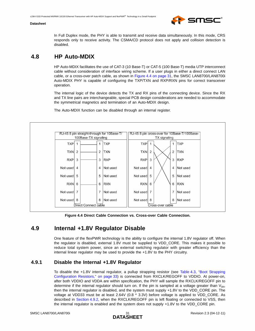
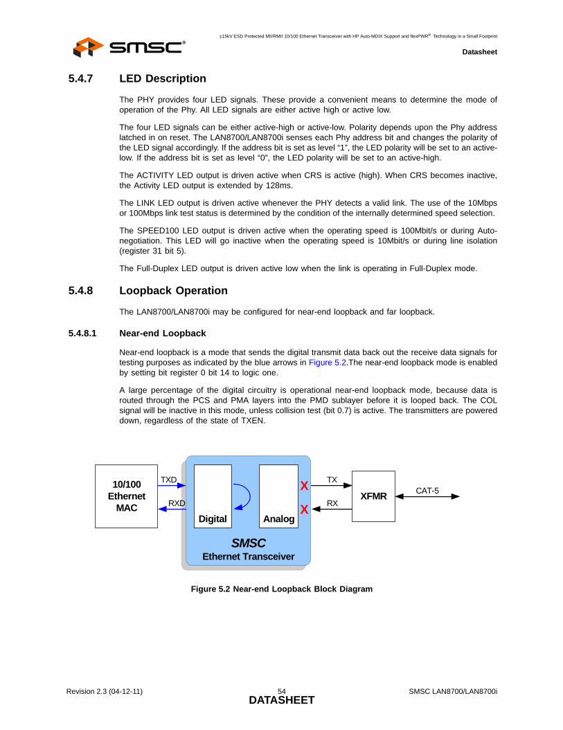
4.8 HP Auto-MDIX HP Auto-MDIX facilitates the use of CAT-3 (10 Base-T) or CAT-5 (100 Base-T) media UTP interconnectcable without consideration of interface wiring scheme. If a user plugs in either a direct connect LANcable, or a cross-over patch cable, as shown in Figure 4.4 on page 31, the SMSC LAN8700/LAN8700iAuto-MDIX PHY is capable of configuring the TXP/TXN and RXP/RXN pins for correct transceiveroperation.
The internal logic of the device detects the TX and RX pins of the connecting device. Since the RXand TX line pairs are interchangeable, special PCB design considerations are needed to accommodatethe symmetrical magnetics and termination of an Auto-MDIX design.
The Auto-MDIX function can be disabled through an internal register.
4.9 Internal +1.8V Regulator DisableOne feature of the flexPWR technology is the ability to configure the internal 1.8V regulator off. Whenthe regulator is disabled, external 1.8V must be supplied to VDD_CORE. This makes it possible toreduce total system power, since an external switching regulator with greater efficiency than theinternal linear regulator may be used to provide the +1.8V to the PHY circuitry.
4.9.1 Disable the Internal +1.8V Regulator
To disable the +1.8V internal regulator, a pullup strapping resistor (see Table 4.3, “Boot StrappingConfiguration Resistors,” on page 33) is connected from RXCLK/REGOFF to VDDIO. At power-on,after both VDDIO and VDDA are within specification, the PHY will sample the RXCLK/REGOFF pin todetermine if the internal regulator should turn on. If the pin is sampled at a voltage greater than VIH,then the internal regulator is disabled, and the system must supply +1.8V to the VDD_CORE pin. Thevoltage at VDD33 must be at least 2.64V (0.8 * 3.3V) before voltage is applied to VDD_CORE. Asdescribed in Section 4.9.2, when the RXCLK/REGOFF pin is left floating or connected to VSS, thenthe internal regulator is enabled and the system does not supply +1.8V to the VDD_CORE pin.
Figure 4.4 Direct Cable Connection vs. Cross-over Cable Connection.
±15kV ESD Protected MII/RMII 10/100 Ethernet Transceiver with HP Auto-MDIX Support and flexPWR® Technology in a Small Footprint
Datasheet
When the +1.8V internal regulator is disabled, a 0.1uF capacitor must be added at the VDD_COREpin and placed close to the PHY to decouple the external power supply.
4.9.2 Enable the Internal +1.8V Regulator
The 1.8V for VDD_CORE is supplied by the on-chip regulator unless the PHY is configured forregulator off mode using the RX_CLK/REGOFF pin as described in Section 4.9.1. By default, theinternal +1.8V regulator is enabled when the RXCLK/REGOFF pin is floating. As shown in Table 7.11,an internal pull-down resistor straps the regulator on if the RXCLK/REGOFF pin is floating.
During VDDIO and VDDA power-on, if the RXCLK/REGOFF pin is sampled below VIL, then the internal+1.8V regulator will turn on and operate with power from the VDD33 pin.
When using the internal linear regulator, a 4.7uF bypass capacitor with ESR < 1ohm and a 0.1uFcapacitor must always be added to VDD_CORE and placed close to the PHY to ensure stability of theinternal regulator.
4.10 nINT/TX_ER/TXD4 StrappingThe nINT, TX_ER, and TXD4 functions share a common pin. There are two functional modes for thispin, the TX_ER/TXD4 mode and nINT (interrupt) mode. The RXD3/nINTSEL pin is used to select oneof these two functional modes.
The RXD3/nINTSEL pin is latched on the rising edge of the nRST. The system designer must float thenINTSEL pin to put the nINT/TX_ER/TXD4 pin into nINT mode or pull-low to VSS with an externalresistor (see Table 4.3, “Boot Strapping Configuration Resistors,” on page 33) to set the device inTX_ER/TXD4 mode. The default setting is to float the pin high for nINT mode.
4.11 PHY Address Strapping and LED Output Polarity SelectionThe PHY ADDRESS bits are latched on the rising edge of the internal reset (nRESET). The 5-bitaddress word[0:4] is input on the PHYAD[0:4] pins. The default setting is all high 5'b1_1111.
The address lines are strapped as defined in the diagram below. The LED outputs will automaticallychange polarity based on the presence of an external pull-down resistor. If the LED pin is pulled high(by an internal 100K pull-up resistor) to select a logical high PHY address, then the LED output willbe active low. If the LED pin is pulled low (by an external pull-down resistor (see Table 4.3, “BootStrapping Configuration Resistors,” on page 33) to select a logical low PHY address, the LED outputwill then be an active high output.
To set the PHY address on the LED pins without LEDs or on the CRS pin, float the pin to set theaddress high or pull-down the pin with an external resistor (see Table 4.3, “Boot StrappingConfiguration Resistors,” on page 33) to GND to set the address low. See Figure 4.5, "PHY AddressStrapping on LED’s":
±15kV ESD Protected MII/RMII 10/100 Ethernet Transceiver with HP Auto-MDIX Support and flexPWR® Technology in a Small Footprint
Datasheet
Figure 4.5 PHY Address Strapping on LED’s
4.12 Variable Voltage I/OThe Digital I/O pins on the LAN8700/LAN8700i are variable voltage to take advantage of low powersavings from shrinking technologies. These pins can operate from a low I/O voltage of +1.8V-10% upto +3.3V+10%. Due to this low voltage feature addition, the system designer needs to takeconsideration as for two aspects of their design. Boot strapping configuration and I/O voltage stability.
4.12.1 Boot Strapping Configuration
Due to a lower I/O voltage, a lower strapping resistor needs to be used to ensure the strappedconfiguration is latched into the PHY device at power-on reset.
.
4.12.2 I/O Voltage Stability
The I/O voltage the System Designer applies on VDDIO needs to maintain its value with a toleranceof ± 10%. Varying the voltage up or down, after the PHY has completed power-on reset can causeerrors in the PHY operation.
4.13 PHY Management ControlThe Management Control module includes 3 blocks:
±15kV ESD Protected MII/RMII 10/100 Ethernet Transceiver with HP Auto-MDIX Support and flexPWR® Technology in a Small Footprint
Datasheet
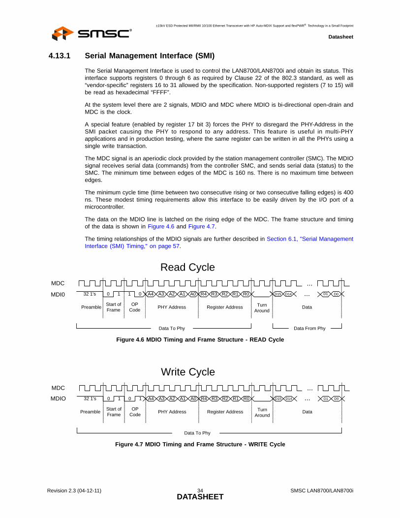
4.13.1 Serial Management Interface (SMI)
The Serial Management Interface is used to control the LAN8700/LAN8700i and obtain its status. Thisinterface supports registers 0 through 6 as required by Clause 22 of the 802.3 standard, as well as“vendor-specific” registers 16 to 31 allowed by the specification. Non-supported registers (7 to 15) willbe read as hexadecimal “FFFF”.
At the system level there are 2 signals, MDIO and MDC where MDIO is bi-directional open-drain andMDC is the clock.
A special feature (enabled by register 17 bit 3) forces the PHY to disregard the PHY-Address in theSMI packet causing the PHY to respond to any address. This feature is useful in multi-PHYapplications and in production testing, where the same register can be written in all the PHYs using asingle write transaction.
The MDC signal is an aperiodic clock provided by the station management controller (SMC). The MDIOsignal receives serial data (commands) from the controller SMC, and sends serial data (status) to theSMC. The minimum time between edges of the MDC is 160 ns. There is no maximum time betweenedges.
The minimum cycle time (time between two consecutive rising or two consecutive falling edges) is 400ns. These modest timing requirements allow this interface to be easily driven by the I/O port of amicrocontroller.
The data on the MDIO line is latched on the rising edge of the MDC. The frame structure and timingof the data is shown in Figure 4.6 and Figure 4.7.
The timing relationships of the MDIO signals are further described in Section 6.1, "Serial ManagementInterface (SMI) Timing," on page 57.
Figure 4.6 MDIO Timing and Frame Structure - READ Cycle
Figure 4.7 MDIO Timing and Frame Structure - WRITE Cycle
±15kV ESD Protected MII/RMII 10/100 Ethernet Transceiver with HP Auto-MDIX Support and flexPWR® Technology in a Small Footprint
Datasheet
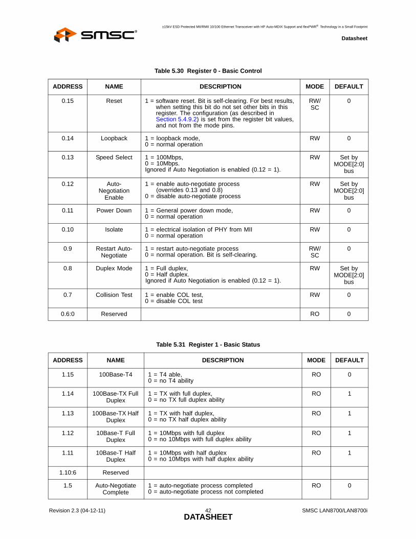
Table 5.30 Register 0 - Basic Control
ADDRESS NAME DESCRIPTION MODE DEFAULT
0.15 Reset 1 = software reset. Bit is self-clearing. For best results, when setting this bit do not set other bits in this register. The configuration (as described in Section 5.4.9.2) is set from the register bit values, and not from the mode pins.
RW/SC
0
0.14 Loopback 1 = loopback mode,0 = normal operation
RW 0
0.13 Speed Select 1 = 100Mbps,0 = 10Mbps.Ignored if Auto Negotiation is enabled (0.12 = 1).
RW Set by MODE[2:0]
bus
0.12 Auto-Negotiation
Enable
1 = enable auto-negotiate process(overrides 0.13 and 0.8)
0 = disable auto-negotiate process
RW Set by MODE[2:0]
bus
0.11 Power Down 1 = General power down mode,0 = normal operation
RW 0
0.10 Isolate 1 = electrical isolation of PHY from MII0 = normal operation
RW 0
0.9 Restart Auto-Negotiate
1 = restart auto-negotiate process0 = normal operation. Bit is self-clearing.
RW/SC
0
0.8 Duplex Mode 1 = Full duplex,0 = Half duplex.Ignored if Auto Negotiation is enabled (0.12 = 1).
RW Set by MODE[2:0]
bus
0.7 Collision Test 1 = enable COL test,0 = disable COL test
RW 0
0.6:0 Reserved RO 0
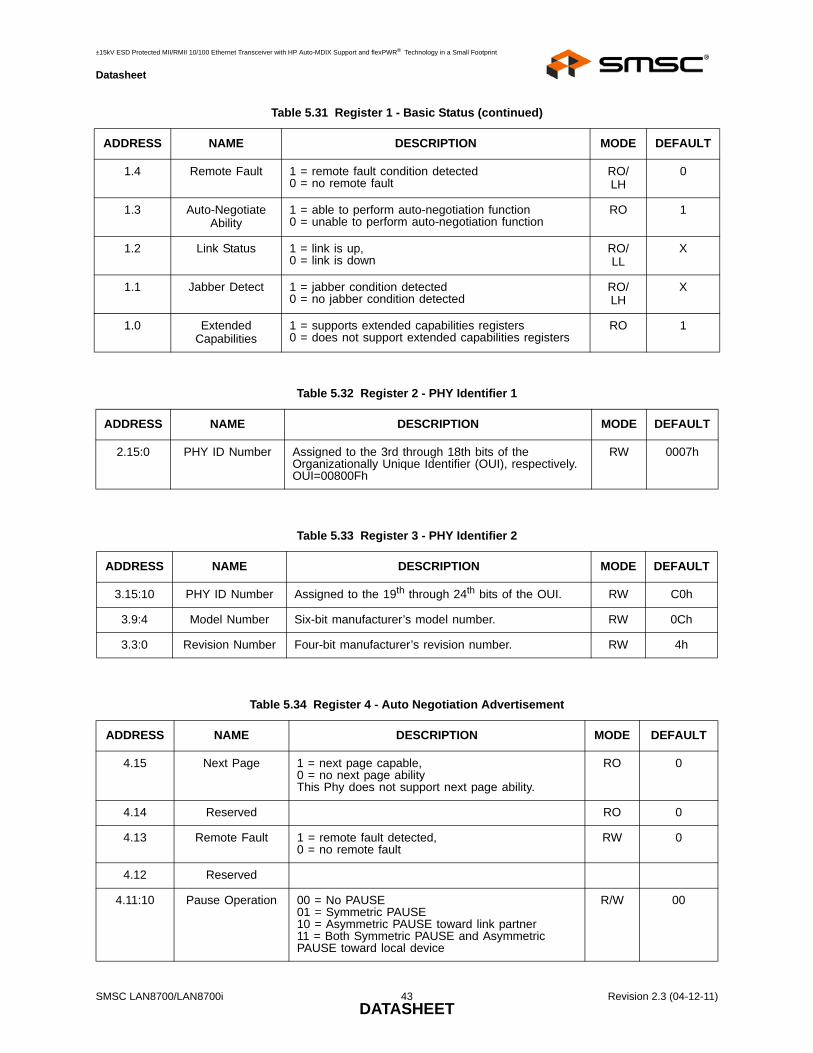
Table 5.31 Register 1 - Basic Status
ADDRESS NAME DESCRIPTION MODE DEFAULT
1.15 100Base-T4 1 = T4 able,0 = no T4 ability
RO 0
1.14 100Base-TX Full Duplex
1 = TX with full duplex,0 = no TX full duplex ability
RO 1
1.13 100Base-TX Half Duplex
1 = TX with half duplex,0 = no TX half duplex ability
RO 1
1.12 10Base-T Full Duplex
1 = 10Mbps with full duplex0 = no 10Mbps with full duplex ability
RO 1
1.11 10Base-T Half Duplex
1 = 10Mbps with half duplex0 = no 10Mbps with half duplex ability
RO 1
1.10:6 Reserved
1.5 Auto-Negotiate Complete
1 = auto-negotiate process completed0 = auto-negotiate process not completed
4.11:10 Pause Operation 00 = No PAUSE01 = Symmetric PAUSE10 = Asymmetric PAUSE toward link partner11 = Both Symmetric PAUSE and AsymmetricPAUSE toward local device
17.15:14 Reserved Write as 0; ignore on read. RW 0
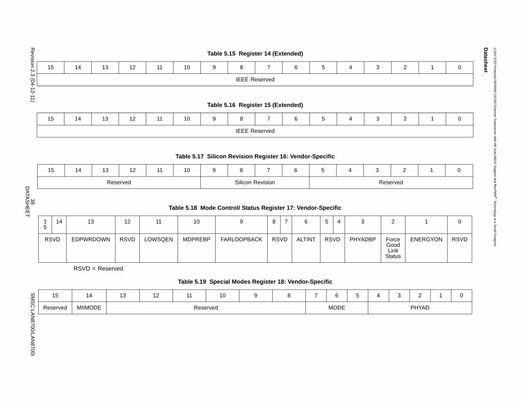
17.13 EDPWRDOWN Enable the Energy Detect Power-Down mode:0 = Energy Detect Power-Down is disabled1 = Energy Detect Power-Down is enabled
RW 0
17.12 Reserved Write as 0, ignore on read RW 0
17.11 LOWSQEN The Low_Squelch signal is equal to LOWSQEN AND EDPWRDOWN.Low_Squelch = 1 implies a lower threshold
(more sensitive).Low_Squelch = 0 implies a higher threshold
(less sensitive).
RW 0
17.10 MDPREBP Management Data Preamble Bypass:0 – detect SMI packets with Preamble1 – detect SMI packets without preamble
RW 0
17.9 FARLOOPBACK Force the module to the FAR Loop Back mode, i.e. all the received packets are sent back simultaneously (in 100Base-TX only). This bit is only active in RMII mode. In this mode the user needs to supply a 50MHz clock to the PHY. This mode works even if MII Isolate (0.10) is set.
±15kV ESD Protected MII/RMII 10/100 Ethernet Transceiver with HP Auto-MDIX Support and flexPWR® Technology in a Small Footprint
Datasheet
Note 5.1 The default value of this field is determined by the strapping of the COL/RMII/CRS_DVpin. Refer to Section 4.6.3, "MII vs. RMII Configuration," on page 28 for additionalinformation.
17.8:7 Reserved Write as 0, ignore on read. RW 00
17.6 ALTINT Alternate Interrupt Mode.0 = Primary interrupt system enabled (Default).1 = Alternate interrupt system enabled.See Section 5.3, "Interrupt Management," on page 49.
0 = normal operation;1 = force 100TX- link active;Note: This bit should be set only during lab testing
RW 0
17.1 ENERGYON ENERGYON – indicates whether energy is detected on the line (see Section 5.4.5.2, "Energy Detect Power-Down," on page 52); it goes to “0” if no valid energy is detected within 256ms. Reset to “1” by hardware reset, unaffected by SW reset.
RO X
17.0 Reserved Write as 0. Ignore on read. RW 0
Table 5.39 Register 18 - Special Modes
ADDRESS NAME DESCRIPTION MODE DEFAULT
18.15 Reserved Write as 0, ignore on read. RW 0
18.14 MIIMODE MII Mode: Reflects the mode of the digital interface:0 – MII interface.1 – RMII interfaceNote: When writing to this register, the default
value of this bit must always be written back.
RW, NASR
Note 5.1
18.13:8 Reserved Write as 0, ignore on read. RW, NASR
000000
18.7:5 MODE PHY Mode of operation. Refer to Section 5.4.9.2, "Mode Bus – MODE[2:0]," on page 56 for more details.
RW, NASR
XXXEVB8700
default 111
18.4:0 PHYAD PHY Address.The PHY Address is used for the SMI address and for the initialization of the Cipher (Scrambler) key. Refer to Section 5.4.9.1, "Physical Address Bus - PHYAD[4:0]," on page 56 for more details.
±15kV ESD Protected MII/RMII 10/100 Ethernet Transceiver with HP Auto-MDIX Support and flexPWR® Technology in a Small Footprint
Datasheet
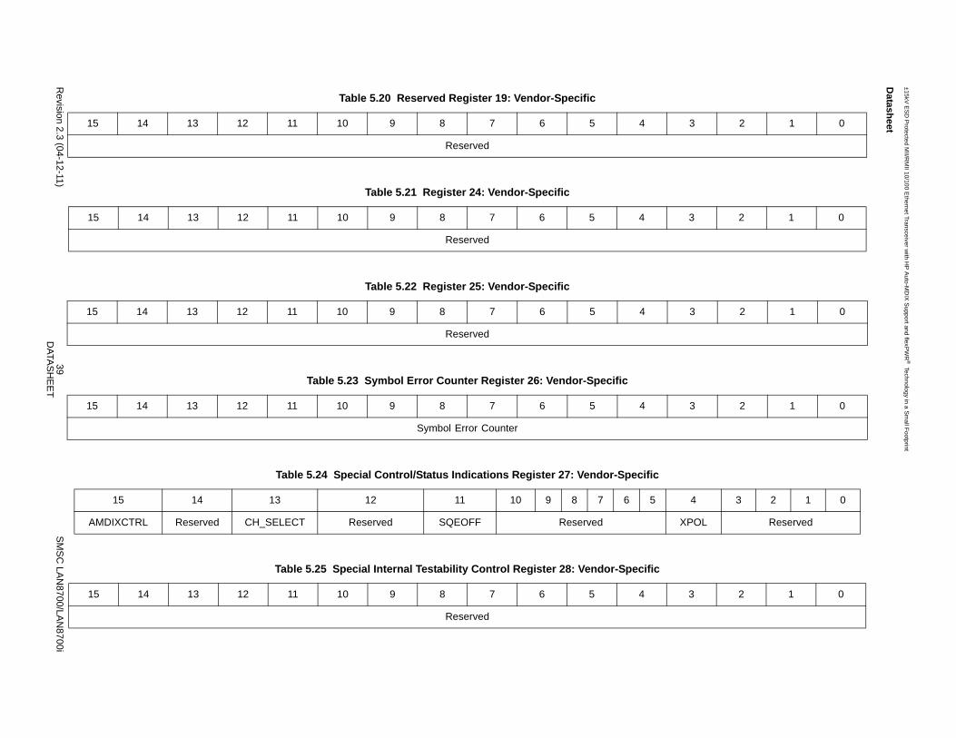
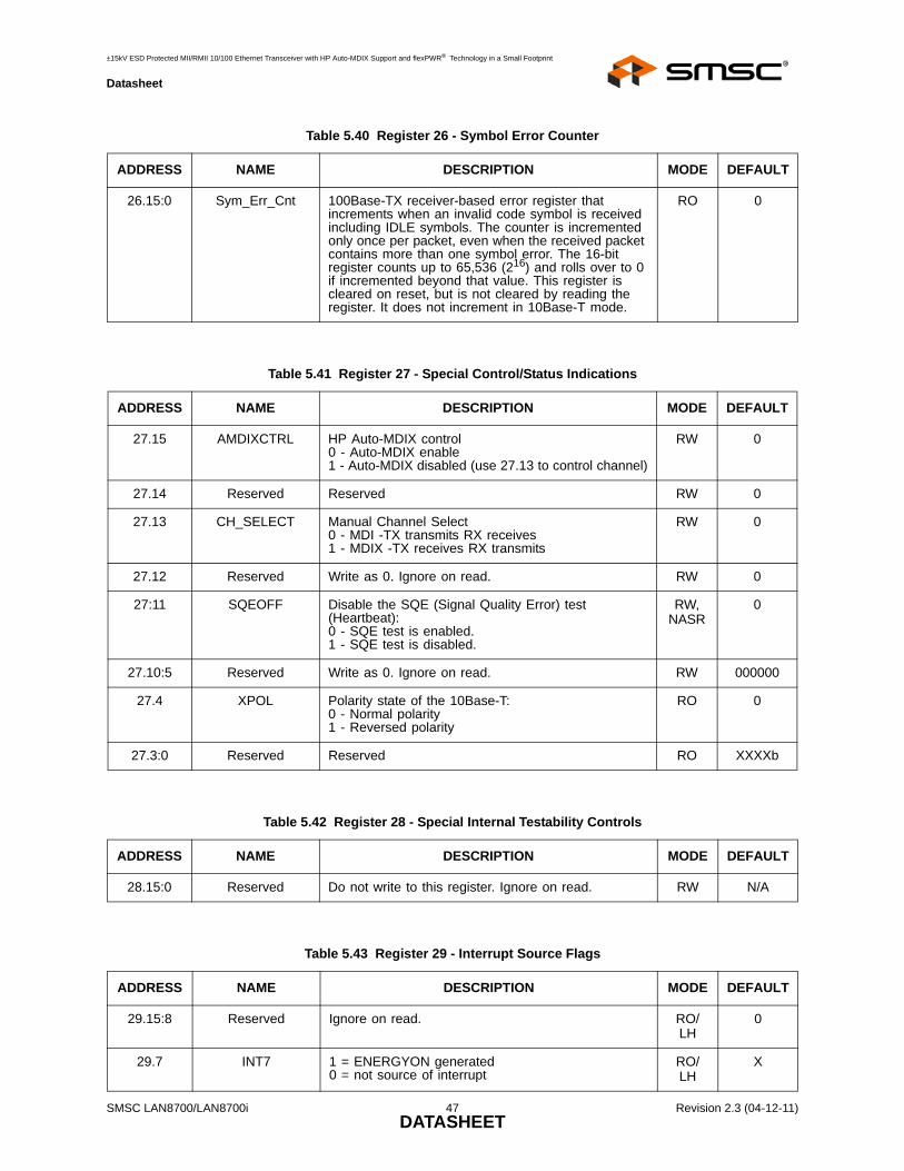
Table 5.40 Register 26 - Symbol Error Counter
ADDRESS NAME DESCRIPTION MODE DEFAULT
26.15:0 Sym_Err_Cnt 100Base-TX receiver-based error register that increments when an invalid code symbol is received including IDLE symbols. The counter is incremented only once per packet, even when the received packet contains more than one symbol error. The 16-bit register counts up to 65,536 (216) and rolls over to 0 if incremented beyond that value. This register is cleared on reset, but is not cleared by reading the register. It does not increment in 10Base-T mode.
RO 0
Table 5.41 Register 27 - Special Control/Status Indications
ADDRESS NAME DESCRIPTION MODE DEFAULT
27.15 AMDIXCTRL HP Auto-MDIX control0 - Auto-MDIX enable1 - Auto-MDIX disabled (use 27.13 to control channel)
±15kV ESD Protected MII/RMII 10/100 Ethernet Transceiver with HP Auto-MDIX Support and flexPWR® Technology in a Small Footprint
Datasheet
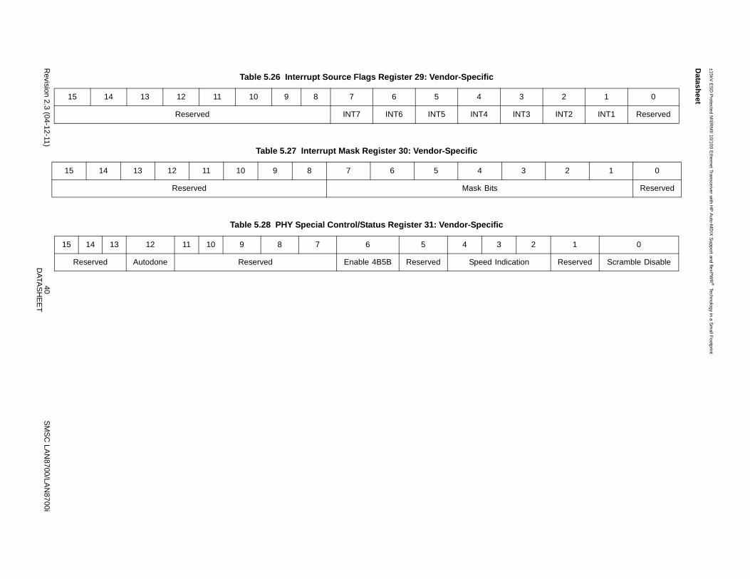
5.3 Interrupt ManagementThe Management interface supports an interrupt capability that is not a part of the IEEE 802.3specification. It generates an active low asynchronous interrupt signal on the nINT output whenevercertain events are detected as setup by the Interrupt Mask Register 30.
The Interrupt system on the SMSC LAN8700/8700I has two modes, a Primary Interrupt mode and anAlternative Interrupt mode. Both systems will assert the nINT pin low when the corresponding maskbit is set, the difference is how they de-assert the output interrupt signal nINT.
The Primary interrupt mode is the default interrupt mode after a power-up or hard reset, the Alternativeinterrupt mode would need to be setup again after a power-up or hard reset.
5.3.1 Primary Interrupt System
The Primary Interrupt system is the default interrupt mode, (Bit 17.6 = ‘0’). The Primary InterruptSystem is always selected after power-up or hard reset.
To set an interrupt, set the corresponding mask bit in the interrupt Mask register 30 (see Table 5.46).Then when the event to assert nINT is true, the nINT output will be asserted.
When the corresponding Event to De-Assert nINT is true, then the nINT will be de-asserted.
±15kV ESD Protected MII/RMII 10/100 Ethernet Transceiver with HP Auto-MDIX Support and flexPWR® Technology in a Small Footprint
Datasheet
Note: The ENERGYON bit 17.1 is defaulted to a ‘1’ at the start of the signal acquisition process,therefore the Interrupt source flag 29.7 will also read as a ‘1’ at power-up. If no signal ispresent, then both 17.1 and 29.7 will clear within a few milliseconds.
5.3.2 Alternate Interrupt System
The Alternative method is enabled by writing a ‘1’ to 17.6 (ALTINT).
To set an interrupt, set the corresponding bit of the in the Mask Register 30, (see Table 5.47).
To Clear an interrupt, either clear the corresponding bit in the Mask Register (30), this will de-assertthe nINT output, or Clear the Interrupt Source, and write a ‘1’ to the corresponding Interrupt SourceFlag. Writing a ‘1’ to the Interrupt Source Flag will cause the state machine to check the InterruptSource to determine if the Interrupt Source Flag should clear or stay as a ‘1’. If the Condition to De-Assert is true, then the Interrupt Source Flag is cleared, and the nINT is also de-asserted. If theCondition to De-Assert is false, then the Interrupt Source Flag remains set, and the nINT remainsasserted.
For example 30.7 is set to ‘1’ to enable the ENERGYON interrupt. After a cable is plugged in,ENERGYON (17.1) goes active and nINT will be asserted low.
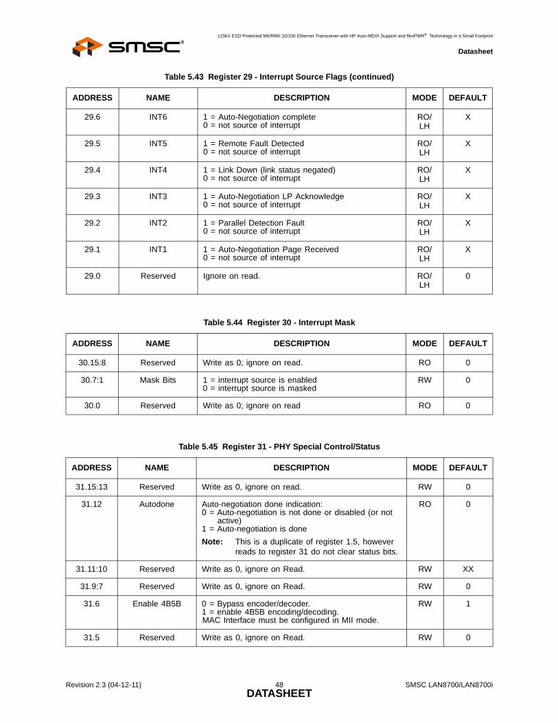
30.5 29.5 Remote Fault Detected 1.4 Remote Fault Rising 1.4 Falling 1.4, or Reading register 1 or Reading register 29
30.4 29.4 Link Down 1.2 Link Status Falling 1.2 Reading register 1 orReading register 29
Rising 6.4 Falling 6.4 or Reading register 6, orReading register 29 orRe-Auto Negotiate or
Link down
30.1 29.1 Auto-Negotiation Page Received
6.1 Page Received Rising 6.1 Falling of 6.1 orReading register 6, orReading register 29
Re-Auto Negotiate, orLink Down.
a. If the mask bit is enabled and nINT has been de-asserted while ENERGYON is still high, nINT will assert for 256 ms, approximately one second after ENERGYON goes low when the Cable is unplugged. To prevent an unexpected assertion of nINT, the ENERGYON interrupt mask should always be cleared as part of the ENERGYON interrupt service routine.
Table 5.46 Interrupt Management Table (continued)
Mask Interrupt Source Flag Interrupt Source Event to Assert nINT Event to De-Assert nINT
±15kV ESD Protected MII/RMII 10/100 Ethernet Transceiver with HP Auto-MDIX Support and flexPWR® Technology in a Small Footprint
Datasheet
To de-assert the nINT interrupt output, either.1. Clear the ENERGYON bit (17.1), by removing the cable, then writing a ‘1’ to register 29.7. Or2. Clear the Mask bit 30.1 by writing a ‘0’ to 30.1.
Note: The ENERGYON bit 17.1 is defaulted to a ‘1’ at the start of the signal acquisition process,therefore the Interrupt source flag 29.7 will also read as a ‘1’ at power-up. If no signal ispresent, then both 17.1 and 29.7 will clear within a few milliseconds.
5.4 Miscellaneous Functions
5.4.1 Carrier Sense
The carrier sense is output on CRS. CRS is a signal defined by the MII specification in the IEEE 802.3ustandard. The PHY asserts CRS based only on receive activity whenever the PHY is either in repeatermode or full-duplex mode. Otherwise the PHY asserts CRS based on either transmit or receive activity.
The carrier sense logic uses the encoded, unscrambled data to determine carrier activity status. Itactivates carrier sense with the detection of 2 non-contiguous zeros within any 10 bit span. Carriersense terminates if a span of 10 consecutive ones is detected before a /J/K/ Start-of Stream Delimiterpair. If an SSD pair is detected, carrier sense is asserted until either /T/R/ End–of-Stream Delimiterpair or a pair of IDLE symbols is detected. Carrier is negated after the /T/ symbol or the first IDLE. If/T/ is not followed by /R/, then carrier is maintained. Carrier is treated similarly for IDLE followed bysome non-IDLE symbol.
5.4.2 Collision Detect
A collision is the occurrence of simultaneous transmit and receive operations. The COL output isasserted to indicate that a collision has been detected. COL remains active for the duration of thecollision. COL is changed asynchronously to both RX_CLK and TX_CLK. The COL output becomesinactive during full duplex mode.
COL may be tested by setting register 0, bit 7 high. This enables the collision test. COL will be assertedwithin 512 bit times of TX_EN rising and will be de-asserted within 4 bit times of TX_EN falling.
In 10M mode, COL pulses for approximately 10 bit times (1us), 2us after each transmitted packet (de-assertion of TX_EN). This is the Signal Quality Error (SQE) signal and indicates that the transmissionwas successful. The user can disable this pulse by setting bit 11 in register 27.
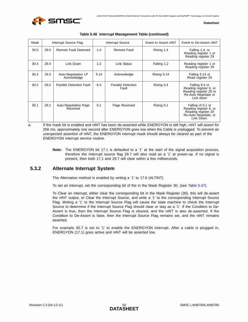
Table 5.47 Alternative Interrupt System Management Table
Mask Interrupt Source Flag Interrupt Source Event to Assert nINT
±15kV ESD Protected MII/RMII 10/100 Ethernet Transceiver with HP Auto-MDIX Support and flexPWR® Technology in a Small Footprint
Datasheet
5.4.3 Isolate Mode
The PHY data paths may be electrically isolated from the MII by setting register 0, bit 10 to a logicone. In isolation mode, the PHY does not respond to the TXD, TX_EN and TX_ER inputs. The PHYstill responds to management transactions.
Isolation provides a means for multiple PHYs to be connected to the same MII without contentionoccurring. The PHY is not isolated on power-up (bit 0:10 = 0).
5.4.4 Link Integrity Test
The LAN8700/LAN8700i performs the link integrity test as outlined in the IEEE 802.3u (Clause 24-15)Link Monitor state diagram. The link status is multiplexed with the 10Mbps link status to form thereportable link status bit in Serial Management Register 1, and is driven to the LINK LED.
The DSP indicates a valid MLT-3 waveform present on the RXP and RXN signals as defined by theANSI X3.263 TP-PMD standard, to the Link Monitor state-machine, using internal signal calledDATA_VALID. When DATA_VALID is asserted the control logic moves into a Link-Ready state, andwaits for an enable from the Auto Negotiation block. When received, the Link-Up state is entered, andthe Transmit and Receive logic blocks become active. Should Auto Negotiation be disabled, the linkintegrity logic moves immediately to the Link-Up state, when the DATA_VALID is asserted.
Note that to allow the line to stabilize, the link integrity logic will wait a minimum of 330 μsec from thetime DATA_VALID is asserted until the Link-Ready state is entered. Should the DATA_VALID input benegated at any time, this logic will immediately negate the Link signal and enter the Link-Down state.
When the 10/100 digital block is in 10Base-T mode, the link status is from the 10Base-T receiver logic.
5.4.5 Power-Down modes
There are 2 power-down modes for the Phy:
5.4.5.1 General Power-Down
This power-down is controlled by register 0, bit 11. In this mode the entire PHY, except themanagement interface, is powered-down and stays in that condition as long as bit 0.11 is HIGH. Whenbit 0.11 is cleared, the PHY powers up and is automatically reset.
5.4.5.2 Energy Detect Power-Down
This power-down mode is activated by setting bit 17.13 to 1. In this mode when no energy is presenton the line the PHY is powered down, except for the management interface, the SQUELCH circuit andthe ENERGYON logic. The ENERGYON logic is used to detect the presence of valid energy from100Base-TX, 10Base-T, or Auto-negotiation signals
In this mode, when the ENERGYON signal is low, the PHY is powered-down, and nothing istransmitted. When energy is received - link pulses or packets - the ENERGYON signal goes high, andthe PHY powers-up. It automatically resets itself into the state it had prior to power-down, and assertsthe nINT interrupt if the ENERGYON interrupt is enabled. The first and possibly the second packetto activate ENERGYON may be lost.
When 17.13 is low, energy detect power-down is disabled.
±15kV ESD Protected MII/RMII 10/100 Ethernet Transceiver with HP Auto-MDIX Support and flexPWR® Technology in a Small Footprint
Datasheet
5.4.6 Reset
The PHY has 3 reset sources:
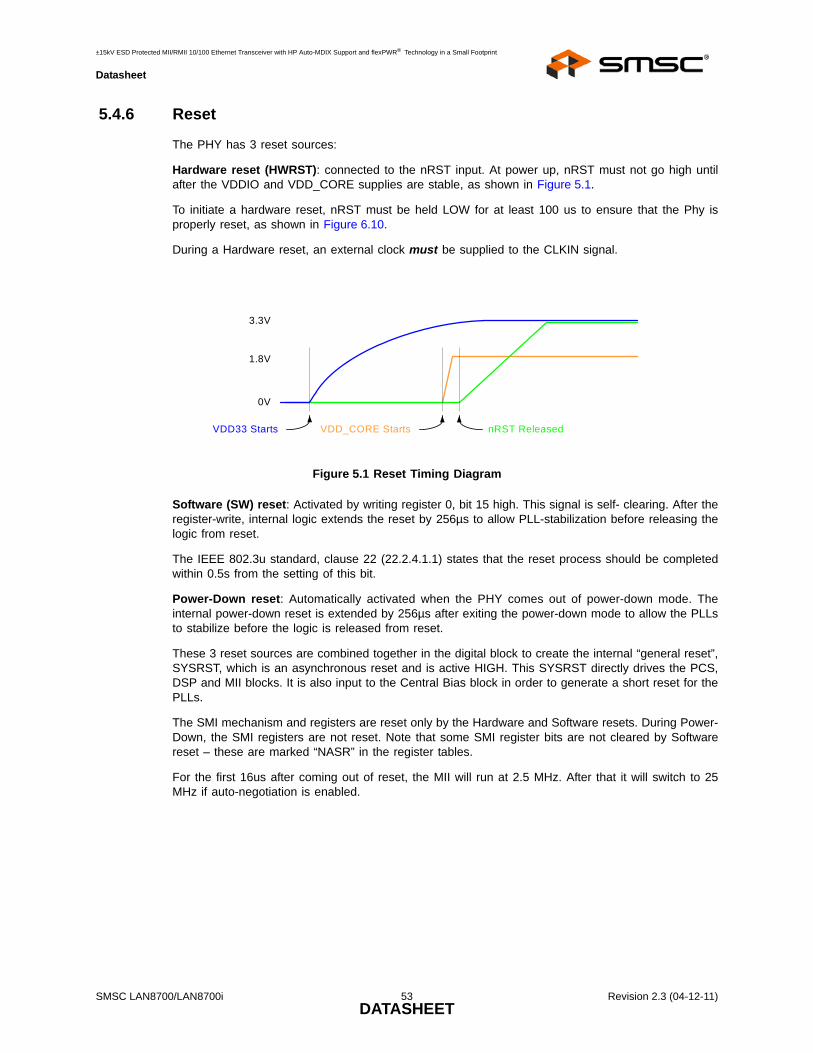
Hardware reset (HWRST): connected to the nRST input. At power up, nRST must not go high untilafter the VDDIO and VDD_CORE supplies are stable, as shown in Figure 5.1.
To initiate a hardware reset, nRST must be held LOW for at least 100 us to ensure that the Phy isproperly reset, as shown in Figure 6.10.
During a Hardware reset, an external clock must be supplied to the CLKIN signal.
Software (SW) reset: Activated by writing register 0, bit 15 high. This signal is self- clearing. After theregister-write, internal logic extends the reset by 256µs to allow PLL-stabilization before releasing thelogic from reset.
The IEEE 802.3u standard, clause 22 (22.2.4.1.1) states that the reset process should be completedwithin 0.5s from the setting of this bit.
Power-Down reset: Automatically activated when the PHY comes out of power-down mode. Theinternal power-down reset is extended by 256µs after exiting the power-down mode to allow the PLLsto stabilize before the logic is released from reset.
These 3 reset sources are combined together in the digital block to create the internal “general reset”,SYSRST, which is an asynchronous reset and is active HIGH. This SYSRST directly drives the PCS,DSP and MII blocks. It is also input to the Central Bias block in order to generate a short reset for thePLLs.
The SMI mechanism and registers are reset only by the Hardware and Software resets. During Power-Down, the SMI registers are not reset. Note that some SMI register bits are not cleared by Softwarereset – these are marked “NASR” in the register tables.
For the first 16us after coming out of reset, the MII will run at 2.5 MHz. After that it will switch to 25MHz if auto-negotiation is enabled.
±15kV ESD Protected MII/RMII 10/100 Ethernet Transceiver with HP Auto-MDIX Support and flexPWR® Technology in a Small Footprint
Datasheet
5.4.7 LED Description
The PHY provides four LED signals. These provide a convenient means to determine the mode ofoperation of the Phy. All LED signals are either active high or active low.
The four LED signals can be either active-high or active-low. Polarity depends upon the Phy addresslatched in on reset. The LAN8700/LAN8700i senses each Phy address bit and changes the polarity ofthe LED signal accordingly. If the address bit is set as level “1”, the LED polarity will be set to an active-low. If the address bit is set as level “0”, the LED polarity will be set to an active-high.
The ACTIVITY LED output is driven active when CRS is active (high). When CRS becomes inactive,the Activity LED output is extended by 128ms.
The LINK LED output is driven active whenever the PHY detects a valid link. The use of the 10Mbpsor 100Mbps link test status is determined by the condition of the internally determined speed selection.
The SPEED100 LED output is driven active when the operating speed is 100Mbit/s or during Auto-negotiation. This LED will go inactive when the operating speed is 10Mbit/s or during line isolation(register 31 bit 5).
The Full-Duplex LED output is driven active low when the link is operating in Full-Duplex mode.
5.4.8 Loopback Operation
The LAN8700/LAN8700i may be configured for near-end loopback and far loopback.
5.4.8.1 Near-end Loopback
Near-end loopback is a mode that sends the digital transmit data back out the receive data signals fortesting purposes as indicated by the blue arrows in Figure 5.2.The near-end loopback mode is enabledby setting bit register 0 bit 14 to logic one.
A large percentage of the digital circuitry is operational near-end loopback mode, because data isrouted through the PCS and PMA layers into the PMD sublayer before it is looped back. The COLsignal will be inactive in this mode, unless collision test (bit 0.7) is active. The transmitters are powereddown, regardless of the state of TXEN.
±15kV ESD Protected MII/RMII 10/100 Ethernet Transceiver with HP Auto-MDIX Support and flexPWR® Technology in a Small Footprint
Datasheet
5.4.8.2 Far Loopback
Far loopback is a special test mode for MDI (analog) loopback as indicated by the blue arrows inFigure 5.3. The far loopback mode is enabled by setting bit register 17 bit 9 to logic one. In this mode,data that is received from the link partner on the MDI is looped back out to the link partner. The digitalinterface signals on the local MAC interface are isolated.
Note: This special test mode is only available when operating in RMII mode.
5.4.8.3 Connector Loopback
The LAN8700/LAN8700i maintains reliable transmission over very short cables, and can be tested ina connector loopback as shown in Figure 5.4. An RJ45 loopback cable can be used to route thetransmit signals an the output of the transformer back to the receiver inputs, and this loopback willwork at both 10 and 100.
Figure 5.3 Far Loopback Block Diagram
Figure 5.4 Connector Loopback Block Diagram
Far-end system
SMSCEthernet Transceiver
10/100Ethernet
MAC
CAT-5XFMR
DigitalRXD
TXD
AnalogRX
TXLink
PartnerX
X
SMSCEthernet Transceiver
10/100Ethernet
MACXFMR
DigitalRXD
TXD
AnalogRX
TX12345678
RJ45 Loopback Cable.Created by connecting pin 1 to pin 3 and connecting pin 2 to pin 6.
±15kV ESD Protected MII/RMII 10/100 Ethernet Transceiver with HP Auto-MDIX Support and flexPWR® Technology in a Small Footprint
Datasheet
5.4.9 Configuration Signals
The PHY has 11 configuration signals whose inputs should be driven continuously, either by externallogic or external pull-up/pull-down resistors.
5.4.9.1 Physical Address Bus - PHYAD[4:0]
The PHYAD[4:0] signals are driven high or low to give each PHY a unique address. This address islatched into an internal register at end of hardware reset. In a multi-PHY application (such as arepeater), the controller is able to manage each PHY via the unique address. Each PHY checks eachmanagement data frame for a matching address in the relevant bits. When a match is recognized, thePHY responds to that particular frame. The PHY address is also used to seed the scrambler. In a multi-PHY application, this ensures that the scramblers are out of synchronization and disperses theelectromagnetic radiation across the frequency spectrum.
5.4.9.2 Mode Bus – MODE[2:0]
The MODE[2:0] bus controls the configuration of the 10/100 digital block. When the nRST pin isdeasserted, the register bit values are loaded according to the MODE[2:0] pins. The 10/100 digitalblock is then configured by the register bit values. When a soft reset occurs (bit 0.15) as described inTable 5.30, the configuration of the 10/100 digital block is controlled by the register bit values, and theMODE[2:0] pins have no affect.
001 10Base-T Full Duplex. Auto-negotiation disabled. 0001 N/A
010 100Base-TX Half Duplex. Auto-negotiation disabled.CRS is active during Transmit & Receive.
1000 N/A
011 100Base-TX Full Duplex. Auto-negotiation disabled.CRS is active during Receive.
1001 N/A
100 100Base-TX Half Duplex is advertised. Auto-negotiation enabled.CRS is active during Transmit & Receive.
1100 0100
101 Repeater mode. Auto-negotiation enabled. 100Base-TX Half Duplex is advertised. CRS is active during Receive.
1100 0100
110 Power Down mode. In this mode the PHY will wake-up in Power-Down mode. The PHY cannot be used when the MODE[2:0] bits are set to this mode. To exit this mode, the MODE bits in Register 18.7:5 (see Table 5.39) must be configured to some other value and a soft reset must be issued.
N/A N/A
111 All capable. Auto-negotiation enabled. X10X 1111
±15kV ESD Protected MII/RMII 10/100 Ethernet Transceiver with HP Auto-MDIX Support and flexPWR® Technology in a Small Footprint
Datasheet
6.6 Clock CircuitLAN8700/LAN8700i can accept either a 25MHz crystal or a 25MHz single-ended clock oscillator(±50ppm) input for operation in MII mode. If the single-ended clock oscillator method is implemented,XTAL2 should be left unconnected and XTAL1/CLKIN should be driven with a nominal 0-3.3V clocksignal. The user is required to supply a 50MHz single-ended clock for RMII operation. The input clockduty cycle is 40% minimum, 50% typical and 60% maximum. See Table 6.12 for the recommendedcrystal specifications.
Note 6.1 The maximum allowable values for Frequency Tolerance and Frequency Stability areapplication dependant. Since any particular application must meet the IEEE ±50 PPM TotalPPM Budget, the combination of these two values must be approximately ±45 PPM(allowing for aging).
Note 6.2 Frequency Deviation Over Time is also referred to as Aging.
Note 6.3 The total deviation for the Transmitter Clock Frequency is specified by IEEE 802.3u as ±100 PPM.
Note 6.4 0oC for commercial version, -40oC for industrial version.
Note 6.5 +70oC for commercial version, +85oC for industrial version.
This number includes the pad, the bond wire and the lead frame. PCB capacitance is not included inthis value. The XTAL1/CLKIN pin, XTAL2 pin and PCB capacitance values are required to accuratelycalculate the value of the two external load capacitors. The total load capacitance must be equivalentto what the crystal expects to see in the circuit so that the crystal oscillator will operate at 25.000 MHz.
±15kV ESD Protected MII/RMII 10/100 Ethernet Transceiver with HP Auto-MDIX Support and flexPWR® Technology in a Small Footprint
Datasheet
Chapter 7 DC Electrical Characteristics
7.1 DC Characteristics
7.1.1 Maximum Guaranteed Ratings
Stresses beyond those listed in may cause permanent damage to the device. Exposure to absolutemaximum rating conditions for extended periods may affect device reliability.
7.1.1.1 Human Body Model (HBM) Performance
HBM testing verifies the ability to withstand the ESD strikes like those that occur during handling andmanufacturing, and is done without power applied to the IC. To pass the test, the device must haveno change in operation or performance due to the event. All pins on the LAN8700 provide ±8kV HBMprotection.
Table 7.1 Maximum Conditions
PARAMETER CONDITIONS MIN TYP MAX UNITS COMMENT
VDD33,VDDIO Power pins to all other pins. -0.5 +3.6 V
Digital IO To VSS ground -0.5 +3.6 V Table 7.5, “MII Bus Interface Signals,” on page 71
VSS VSS to all other pins -0.5 +4.0 V
Operating Temperature
LAN8700-AEZG 0 +70 C Commercial temperature components.
Operating Temperature
LAN8700i-AEZG -40 +85 C Industrial temperature components.
±15kV ESD Protected MII/RMII 10/100 Ethernet Transceiver with HP Auto-MDIX Support and flexPWR® Technology in a Small Footprint
Datasheet
7.1.1.2 IEN/IEC61000-4-2 Performance
The EN/IEC61000-4-2 ESD specification is an international standard that addresses system-levelimmunity to ESD strikes while the end equipment is operational. In contrast, the HBM ESD tests areperformed at the device level with the device powered down.
SMSC contracts with Independent laboratories to test the LAN8700 to EN/IEC61000-4-2 in a workingsystem. Reports are available upon request. Please contact your SMSC representative, and requestinformation on 3rd party ESD test results. The reports show that systems designed with the LAN8700can safely dissipate ±15kV air discharges and ±8kV contact discharges per the EN/IEC61000-4-2specification without additional board level protection.
In addition to defining the ESD tests, EN/IEC61000-4-2 also categorizes the impact to equipmentoperation when the strike occurs (ESD Result Classification). The LAN8700 maintains an ESD ResultClassification 1 or 2 when subjected to an EN/IEC61000-4-2 (level 4) ESD strike.
Both air discharge and contact discharge test techniques for applying stress conditions are defined bythe EN/IEC61000-4-2 ESD document.
AIR DISCHARGE
To perform this test, a charged electrode is moved close to the system being tested until a spark isgenerated. This test is difficult to reproduce because the discharge is influenced by such factors ashumidity, the speed of approach of the electrode, and construction of the test equipment.
CONTACT DISCHARGE
The uncharged electrode first contacts the pin to prepare this test, and then the probe tip is energized.This yields more repeatable results, and is the preferred test method. The independent test laboratoriescontracted by SMSC provide test results for both types of discharge methods.
7.1.2 Operating Conditions
7.1.3 Power Consumption
7.1.3.1 Power Consumption Device Only
Power measurements taken over the operating conditions specified. See Section 5.4.5 for a descriptionof the power down modes.
Table 7.3 Recommended Operating Conditions
PARAMETER CONDITIONS MIN TYP MAX UNITS COMMENT
VDD33 VDD33 to VSS 3.0 3.3 3.6 V
Input Voltage on Digital Pins
0.0 VDDIO V
Voltage on Analog I/O pins (RXP, RXN)
0.0 +3.6V V
Ambient Temperature TA LAN8700-AEZG 0 70 C For Commercial Temperature
TA LAN8700i-AEZG -40 +85 C For Industrial Temperature
±15kV ESD Protected MII/RMII 10/100 Ethernet Transceiver with HP Auto-MDIX Support and flexPWR® Technology in a Small Footprint
Datasheet
Note: The current at VDD_CORE is either supplied by the internal regulator from current entering atVDD33, or from an external 1.8V supply when the internal regulator is disabled.
Note 7.1 This is calculated with full flexPWR features activated: VDDIO = 1.8V and internal regulatordisabled.
Note 7.2 Current measurements do not include power applied to the magnetics or the optionalexternal LEDs. Current measurements taken with VDDIO = +3.3V, unless otherwiseindicated.
±15kV ESD Protected MII/RMII 10/100 Ethernet Transceiver with HP Auto-MDIX Support and flexPWR® Technology in a Small Footprint
Datasheet
Chapter 8 Application Notes
8.1 Application Diagram
Note: R5 on the Crystal is used to control the crystal drive strength into the PHY clock generator.This resistance can be fine tuned to meet the requirements of each crystal manufacturer.
Figure 8.1 Simplified Application Diagram (see Section 8.4, "Reference Designs")
±15kV ESD Protected MII/RMII 10/100 Ethernet Transceiver with HP Auto-MDIX Support and flexPWR® Technology in a Small Footprint
Datasheet
8.2 Magnetics SelectionFor a list of magnetics selected to operate with the SMSC LAN8700, please refer to the Applicationnote “AN 8-13 Suggested Magnetics”.
8.3 Application NotesApplication examples are given in pdf format on the SMSC LAN8700 web site. The link to the web siteis shown below.
http://www.smsc.com/main/catalog/lan8700.html
Please check the web site periodically for the latest updates.
8.4 Reference DesignsThe LAN8700 Reference designs are available on the SMSC LAN8700 web site link below.
http://www.smsc.com/main/catalog/lan8700.html
The reference designs are available in four variations:
a. MII with +3.3V IO b. RMII with +3.3V IO c. MII with +1.8V IO d. RMII with +1.8V IO.
8.5 Evaluation boardThe EVB-LAN8700 is a a PHY Evaluation Board (EVB) that interfaces a MAC controller to the SMSCLAN8700 Ethernet PHY through an MII connector, and out to an RJ-45 Ethernet Jack through industrialtemperature magnetics for 10/100 connectivity.
Schematics(*.pdf and *.dsn), BOM (bill of materials), user guide, gerber files and Layout board file areall available on the EVB web site link below.
http://www.smsc.com/main/catalog/evblan8700.html
The EVB-LAN8700 is designed to plug into a user's test system using a 40 pin Media IndependentInterface (MII) connector. The MII connector is an AMP 40 pin Right Angle through hole MII connector,PN AMP- 174218-2. The mating connector is PN AMP 174217-2.
FEATURES:
Industrial temperature PHY and Magnetics
8 pin SOIC for user configurable Magnetics
On board LED indicators for Speed 100
Full Duplex
RJ-45 Connector LEDs for Link and Activity
Interfaces Through 40-pin Connector as Defined in the MII Specification
Powered by 5.0V from the 40-Pin MII Connector
Standard RJ45 Connector with LED indicators for Link and Activity
Includes Probe Points on All MII Data and Control Signals for Troubleshooting
±15kV ESD Protected MII/RMII 10/100 Ethernet Transceiver with HP Auto-MDIX Support and flexPWR® Technology in a Small Footprint
Datasheet
Includes 25MHz Crystal for Internal PHY Reference; RX_CLK is Supplied to the 40-Pin Connector
Supports user configuration options including PHY address selection
Integrated 3.3V Regulator
APPLICATIONS
The EVB8700 Evaluation board simplifies the process of testing and evaluating an EthernetConnection in your application. The LAN8700 device is installed on the EVB board and all associatedcircuitry is included, along with all configuration options.
The Benefits of adding an external MII interface are:
±15kV ESD Protected MII/RMII 10/100 Ethernet Transceiver with HP Auto-MDIX Support and flexPWR® Technology in a Small Footprint
Datasheet
Chapter 9 Package Outline, Tape and Reel
Figure 9.1 36-Pin QFN Package Outline, 6 x 6 x 0.90 mm Body (Lead-Free)
Notes:1. Controlling Unit: millimeter.
2. Dimension b applies to plated terminals and is measured between 0.15mm and 0.30mm from theterminal tip. Tolerance on the true position of the terminal is ± 0.05 mm at maximum materialconditions (MMC).
3. Details of terminal #1 identifier are optional but must be located within the zone indicated.4. Coplanarity zone applies to exposed pad and terminals.
Table 9.1 36-Pin QFN Package Parameters
MIN NOMINAL MAX REMARKSA 0.80 ~ 1.00 Overall Package HeightA1 0 ~ 0.05 StandoffA2 0.60 ~ 0.80 Mold ThicknessA3 0.20 REF Copper Lead-frame Substrate D 5.85 ~ 6.15 X Overall Size
D1 5.55 ~ 5.95 X Mold Cap SizeD2 3.55 ~ 3.85 X exposed Pad SizeE 5.85 ~ 6.15 Y Overall SizeE1 5.55 ~ 5.95 Y Mold Cap SizeE2 3.55 ~ 3.85 Y exposed Pad SizeL 0.35 ~ 0.75 Terminal Lengthe 0.50 Basic Terminal Pitchb 0.18 ~ 0.30 Terminal Width
±15kV ESD Protected MII/RMII 10/100 Ethernet Transceiver with HP Auto-MDIX Support and flexPWR® Technology in a Small Footprint
Datasheet
Chapter 10 Datasheet Revision History
Table 10.1 Customer Revision History
REVISION LEVEL & DATE SECTION/FIGURE/ENTRY CORRECTION
Rev. 2.3(04-12-11)
Section 6.5, "Reset Timing," on page 66
Corrected T11.4 minimum value to 3ns.Corrected T11.3 to 2ns.
Table 5.39, “Register 18 - Special Modes,” on page 46
Updated MIIMODE bit description and added note: “When writing to this register, the default value of this bit must always be written back.”Added note regarding default MIIMODE value.
Section 4.6.3, "MII vs. RMII Configuration," on page 28
Updated section to remove information about register control of the MII/RMII mode.
Section 5.4.8.2, "Far Loopback," on page 55
Updated section to remove information about register control of the MII/RMII mode.
Rev. 2.2(12-04-09)
Table 6.1, "SMI Timing Values" Updated T1.2 maximum to 300ns.
Rev. 2.1(03-06-09)
Section 5.4.6 Removed reference to internal POR system. Added note the nRST should be low until VDDIO and VDD_CORE are stable. Added Figure.
Table 5.34 Corrected bit value for Asymmetric and Symmetric PAUSE.
Section 6.3 Improved timing values.
Section 5.4.8 Enhanced this section.
Section 4.6.3 Added information about register bit 18.14.
Section 6.6 Added section on clock, with crystal specification table.
Figure 1.1 Removed GPIO from the LED block.
Section 4.11 Removed reference to GP01 pin in third paragraph.
Table 5.45 Renamed Bits 7-9 as Reserved.
Table 5.28 Renamed Bits 7-9 as Reserved.
Rev. 2.0(07-15-08)
Chapter 9, Package Outline, Tape and Reel
Tape and reel drawings and ordering info added.
Rev. 1.9(03-18-08)
Figure 6.7, "100M RMII Transmit Timing Diagram"
Replaced figure.
Rev. 1.9(03-18-08)
Table 6.5, "10M MII Transmit Timing Values"
Removed the text “T5.2” in the “Parameter” column.
Rev. 1.9(03-18-08)
Figure 6.5, "10M MII Transmit Timing Diagrams"
Replaced figure.
Rev. 1.9(03-18-08)
Table 6.3, "100M MII Transmit Timing Values"
Removed the text “T3.2” in the “Parameter” column.
±15kV ESD Protected MII/RMII 10/100 Ethernet Transceiver with HP Auto-MDIX Support and flexPWR® Technology in a Small Footprint
Datasheet
Rev. 1.9(03-18-08)
Figure 6.3, "100M MII Transmit Timing Diagram"
Replaced figure.
Rev. 1.9(03-18-08)
Table 6.11, "Reset Timing Values" Changed the MIN value for T11.3:From: “400”To: “10”
Rev. 1.9(03-18-08)
Table 6.4, "10M MII Receive Timing Values"
Deleted last row in table.
Rev. 1.9(03-18-08)
Section 4.6.2.1, "Reference Clock" First sentence of second paragraph changed:From: “between 35% and 65%”To: “between 40% and 60%”
Rev. 1.8(02-14-08)
Table 6.7 Changed value of T8.1 and T8.2.
Rev. 1.8(02-14-08)
Table 6.6 Changed value of T6.1.
Rev. 1.6(12-11-07)
Section 4.9 Added information about not applying VDD_CORE before VDD33 is at 2.64V.
Rev. 1.6(12-11-07)
Table 3.8, "Power Signals" Updated description of VDD_CORE for information on using external 1.8V supply.
Rev. 1.6(12-11-07)
Table 3.1, "MII Signals" Updated description of RX_CLK/REGOFF to add power supply sequencing information.
Rev. 1.6(12-11-07)
Table 5.33, "Register 3 - PHY Identifier 2"
Updated Revision Number to match the LAN8700C silicon.
Rev. 1.5(10-04-07)
Chapter 8, Application Notes Figure 8.1 has been updated. In addition, the following cross reference added to caption:(see Section 8.4, "Reference Designs").
Rev. 1.4(09-17-07)
Section 7.1.4 Changed VIH to 0.68*VDDIO.Changed VIL to 0.4*VDDIO.
Rev. 1.3(06-27-07)
Table 6.9 Moved parameter T10.2 in Table 6.9 from MAX column to MIN column.
Rev. 1.3(06-27-07)
Table 6.5 Moved parameter T5.2 in Table 6.5 from MAX column to MIN column.
Rev. 1.2(05-29-07)
Table 5.48 Added description when the MODE[2:0] bits are set to 110.
Rev. 1.2(05-29-07)
Table 5.30 Corrected Default value for bit 0.11 to the value of 0. This bit does not get set when the MODE[2:0] bits are set to 110.
Rev. 1.2(05-23-07)
Section 5.4.9.2 Added detail about MODE[2:0] pins having no affect at soft reset.
Rev. 1.2(05-23-07)
Table 5.30 Added note to reset description (bit 0.15).
Rev. 1.2(05-23-07)
Table 3.5 AT nRST, added note that register bit values are loaded from the Mode pins upon deassertion.
Table 10.1 Customer Revision History (continued)
REVISION LEVEL & DATE SECTION/FIGURE/ENTRY CORRECTION