Silicon Detectors Hartmut F.-W. Sadrozinski , SCIPP, UC Santa Cruz SCIPP Large-Scale Applications of Silicon Detectors in Space Hartmut F.-W. Sadrozinski Santa Cruz Institute for Particle Physics (SCIPP)
Transcript
Silicon Detectors Hartmut F.-W. Sadrozinski , SCIPP, UC Santa Cruz
SCIPPSCIPP
Large-Scale Applications of Silicon Detectorsin Space
Hartmut F.-W. SadrozinskiSanta Cruz Institute for Particle Physics (SCIPP)
Silicon Detectors Hartmut F.-W. Sadrozinski , SCIPP, UC Santa Cruz
SCIPPSCIPP Principle of Silicon Strip Detectors
25-200 µm
300-400 µm
Alat ~ 100V
n+ implant
Al SiO2
p+ implantat ground
Depletion region. Charged particletraversing region produces ~80electron/hole pairs per micron.
Readout electronics(S/N typically > 20)
holes
Reverse Bias of junction: thermal current generationScale : Band gap 1.12eV vs. kT = 1/40eVCooling needed only in ultra-low noise applications.Wafer thickness 300um = 24k e-h pairs = 0.3%RLDepletion Voltage ~ thickness2 <100V Collection Time of e-h pairs: ~30nsArea is given by wafer size: 4” & 6” => Ladders
Silicon Detectors Hartmut F.-W. Sadrozinski , SCIPP, UC Santa Cruz
SCIPPSCIPP Evolution of Silicon Detectors
Large Area Double-sided
Hybrid Pixels
Monolythic:CCD, MAP
Si Drift
3-D
n n n
nn
p p
n
Silicon Detectors Hartmut F.-W. Sadrozinski , SCIPP, UC Santa Cruz
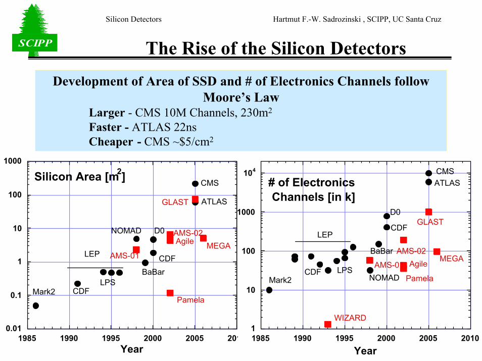
SCIPPSCIPP The Rise of the Silicon Detectors
Development of Area of SSD and # of Electronics Channels follow Moore’s Law
Larger - CMS 10M Channels, 230m2
Faster - ATLAS 22nsCheaper - CMS ~$5/cm2
0.01
0.1
1
10
100
1000
1985 1990 1995 2000 2005 201
Silicon Area [m2]
Year
CDF
ATLASGLAST
CMS
AMS-02
AMS-01
D0
BaBar
NOMAD
LEP
LPSCDFMark2
Pamela
Agile MEGA
1
10
100
1000
104
1985 1990 1995 2000 2005 2010
# of Electronics Channels [in k]
Year
CDF
ATLAS
GLAST
CMS
AMS-02
AMS-01
WIZARD
D0
BaBar
NOMAD
LEP
LPSCDFMark2 Pamela
Agile MEGA
Silicon Detectors Hartmut F.-W. Sadrozinski , SCIPP, UC Santa Cruz
SCIPPSCIPP The Rise of the Silicon Detectors
Edge joint and wire bonds before encapsulation
0.01
0.1
1
10
100
10 100 1000 104
Silicon Area vs. # of Electronics Channels
# of Channels [k]
CDF
ATLASGLAST
CMS
AMS-02
AMS-01 D0
BaBar
NOMAD
LEP
LPSCDF
Mark2 Pamela
Agile MEGA
Are
a[m
2 ]
Limited Resources (Power) in Space
Long Ladders possible with:Bonding and Encapsulation
Silicon Detectors Hartmut F.-W. Sadrozinski , SCIPP, UC Santa Cruz
SCIPPSCIPP The Rise of the Silicon Detectors
Trends in the Cost of Silicon Detectors
Cost of processing wafers reduced ~ 4x
Increased Area 4” -> 6”Better utilisation of area
Improved Qualitye.g. GLAST detectors:
<2nA/ cm2
<2*10-4 bad channels 1
10
100
1985 1990 1995 2000
Cost /Area of Single-sided Silicon Strip Detectors(double-sided factor 2.5 higher)
4"6"
Cos
t /A
rea
[ $/c
m2 ]
Year
Mark 2DC coupl.
ZEUSDC coupl.
CDFNomad
(untested)
GLAST"4"
ATLAS
GLAST6"
Wafer Size
Blank Wafer Price4 "
6 "
CMS
(Guestimates by HFWS)
Silicon Detectors Hartmut F.-W. Sadrozinski , SCIPP, UC Santa Cruz
SCIPPSCIPP Tracking Milestones: Fixed Target
Silicon Detectors~ 5cm x5cm
Fanout-Cables
Amplifiers
That’s how it all began
Fixed Target experiments withhigh rates:
Na11 (ACCMOR)Na14E706E691
Detect heavy decaying particles through their finite decay distance
Silicon Detectors Hartmut F.-W. Sadrozinski , SCIPP, UC Santa Cruz
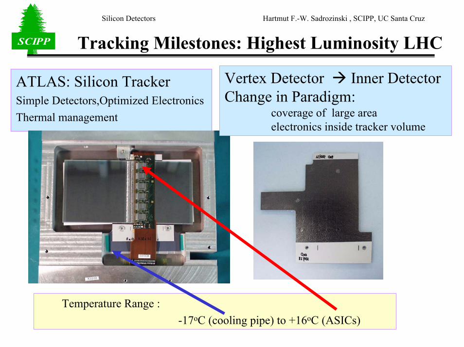
SCIPPSCIPP Tracking Milestones: Vertex Detectors
The big step forward in Mark2:ASIC’s (Terry Walker et al)
Vertex Detector ParadigmASIC’s,Few thin layers,Close in.
ALEPH
Every LEP Experiment has aVertex Detectors:
Double-SidedAC-coupled
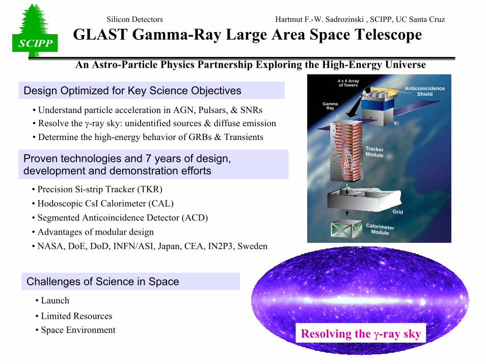
Silicon Detectors Hartmut F.-W. Sadrozinski , SCIPP, UC Santa Cruz
• Understand particle acceleration in AGN, Pulsars, & SNRs• Resolve the γ-ray sky: unidentified sources & diffuse emission• Determine the high-energy behavior of GRBs & Transients
Proven technologies and 7 years of design, development and demonstration efforts
Silicon Detectors Hartmut F.-W. Sadrozinski , SCIPP, UC Santa Cruz
SCIPPSCIPP Criteria for large-scale Application in Space:
FlexibilityAdapt to Space EnvironmentUse Conservative Approach
ModularityClean InterfacesLow risk in Performance and Schedule
RedundancyNo single-point failures
Q/AParts SelectionProceduresEarly R&DTesting
Silicon Detectors Hartmut F.-W. Sadrozinski , SCIPP, UC Santa Cruz
SCIPPSCIPP The Large Area Telescope (LAT)
DAQ Electronics
Grid
Tracker
Calorimeter
ACD Thermal Blanket
•Array of 16 identical “Tower” Modules, each with a tracker (Si strips) and a calorimeter (CsI with PIN diode readout) and DAQ module.
•Surrounded by finely segmented ACD(plastic scintillator with PMT readout).
•Aluminum strong-back “Grid,” with heat pipes for transport of heat to the instrument sides.
Silicon Detectors Hartmut F.-W. Sadrozinski , SCIPP, UC Santa Cruz
SCIPPSCIPP GLAST LAT: International Collaboration• expertise in each science topic (theory + obs.)• experience in high-energy and space instrumentation• access to X-ray, MeV, and TeV observatories by
collaboration for multi-wavelength observations
• expertise in each science topic (theory + obs.)• experience in high-energy and space instrumentation• access to X-ray, MeV, and TeV observatories by
collaboration for multi-wavelength observations
~ 100 collaboratorsfrom 28 institutions
~ 100 collaboratorsfrom 28 institutions
Organizations with LAT Hardware Involvement
Stanford University & Stanford Linear Accelerator CenterNASA Goddard Space Flight CenterNaval Research LaboratoryUniversity of California at Santa CruzUniversity of Washington
Commissariat a l’Energie Atomique, Departement d’Astrophysique (CEA)Institut National de Physique Nuclearie et de Physique des Particules (IN2P3): Ecole Polytechnique, College de France, CENBG (Bordeaux)
Hiroshima UniversityInstitute of Space and Astronautical Science, TokyoRIKENTokyo Institute of Technology
Istituto Nazionale di Fisica Nucleare (INFN): Pisa, Trieste, Bari, Udine, Perugia, Roma
Royal Institute of Technology (KTH), Stockholm
TKRCALACD
CAL
TKR
TKR
CAL
Silicon Detectors Hartmut F.-W. Sadrozinski , SCIPP, UC Santa Cruz
SCIPPSCIPP GLAST LAT TKR
• Numbers: GLAST is modular:16 flight (+ 2 calibration towers) with 18 x-y SSD planes each4 x 4 SSD per plane ( 4 ladders with 4 SSD each)Number of SSD needed:
Butt-join and wire-bond 4 SSD to “ladders”Glue 4 Ladders onto both sides of 3cm thick panels (“trays”) Attach MCM on the side of the panel via 90o interconnect Stack trays into towers
• QA:Tight specification increase reliability of SSDCharge manufacturer with all detailed testingTest important parameters before further integration step
Silicon Detectors Hartmut F.-W. Sadrozinski , SCIPP, UC Santa Cruz
SCIPPSCIPP Overview of TKR Tower Design
• 16 towers, each with 37 cm × 37 cm of Si (78m2 in all)
• 18 x,y planes per tower– 19 “tray” structures ~3cm high
• Si planes on top and bottom• 12 with 3% W converter on bottom• 4 with 25% W converter on bottom• 2 with no converter
– Every other tray rotated by 90°, so each W foil is followed immediately by an x,yplane
• 2mm gap between x and y• Electronics on the sides of trays
– Minimize gap between towers– 9 readout modules on each of 4 sides
• Trays stack and align at their corners• The bottom tray has a flange to mount on
the grid• Carbon-fiber walls provide stiffness and
the thermal pathway to the grid
Carbon thermal
panel
Readout Cable
Electronics Module
2 mm gapCarbon-Fiber Wall
19 Carbon-Fiber Tray Panels
Silicon Detectors Hartmut F.-W. Sadrozinski , SCIPP, UC Santa Cruz
SCIPPSCIPP TKR Flight-Tower Design & Assembly
Cable PlantUCSC
SSD Procurement, TestingJapan, Italy, SLAC
Electronics Design, Fabrication & TestUCSC, SLAC
Tower Assembly and TestSLAC (2) Italy (16)
Tray Assembly and TestItaly
SSD Ladder AssemblyItaly
Composite Panel & ConvertersEngineering: SLAC, Hytec, and ItalyProcurement: Italy
Silicon Detectors Hartmut F.-W. Sadrozinski , SCIPP, UC Santa Cruz
SCIPPSCIPP 6” wafer of the GLAST SSD
Each wafer has a GLAST2000 SSD and a GLAST cut-off.We have established the correlation between SSD and test structure performance.
GLAST Test Structures“Baby”, 32 strips, 3.5cmMos Structures Bonding Test StructurePhoto Diodes“Skinny”,8 strips, full length,
GLAST2000 SSD8.95cm x 8.95cm
Silicon Detectors Hartmut F.-W. Sadrozinski , SCIPP, UC Santa Cruz
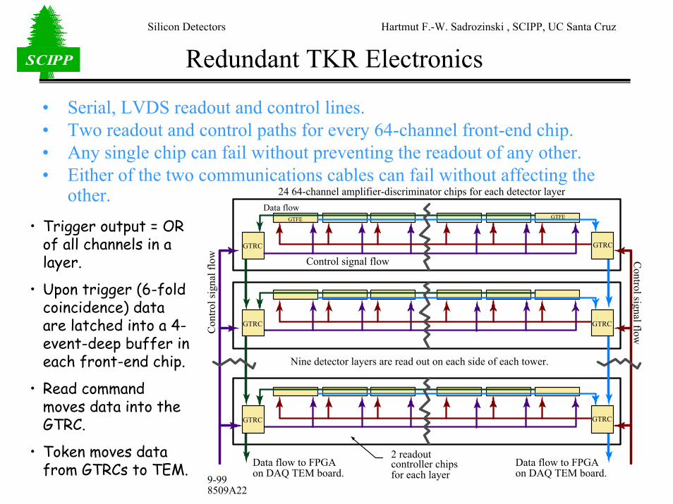
SCIPPSCIPP Redundant TKR Electronics
• Serial, LVDS readout and control lines.• Two readout and control paths for every 64-channel front-end chip.• Any single chip can fail without preventing the readout of any other.• Either of the two communications cables can fail without affecting the
other. 24 64-channel amplifier-discriminator chips for each detector layer
2 readoutcontroller chipsfor each layer
Con
trol s
igna
l flo
w Control signal flow
Data flow to FPGAon DAQ TEM board.
Data flow to FPGAon DAQ TEM board.
Control signal flow
Data flow
Nine detector layers are read out on each side of each tower.
GTRC
GTFEGTFE
GTRC
GTRC
GTRC
GTRC
GTRC
9-998509A22
• Trigger output = OR of all channels in a layer.
• Upon trigger (6-fold coincidence) data are latched into a 4-event-deep buffer in each front-end chip.
• Read command moves data into the GTRC.
• Token moves data from GTRCs to TEM.
Silicon Detectors Hartmut F.-W. Sadrozinski , SCIPP, UC Santa Cruz
SCIPPSCIPP 2 Clean TKR Interfaces per Tower
4.1.4.3.1Silicon-Strip
Detectors
4.1.4.3.2Tray Mechanical
C-fiber panelW converters
4.1.4.3.3Tray Electronics (MCM)
F.E. ASIC; Controller ASIC; PC Board;Connector sockets; Pitch Adapter; Passive parts
4.1.4.4.1Tower Structure
C-fiber sidewallsFasteners
Spacers/pinsEMI shield
4.1.4.4.2Tower Cable Plant
Flexible multi-layer cables; Connector Plugs
Wire BondsScrews;
Adhesive tape
BiasCircuit;
Adhesive
Det
ecto
r Bia
s
Wire
Bon
ds
Nano- Connectors Machined
Cable RunsFasteners
TowerElectronics
Module
GridFlexure Mount
ThermalGasket
GLAST TrackerBlock Diagram
andInterfaces
Mechanical
ElectricalNo Inter-Tower Interfaces
Silicon Detectors Hartmut F.-W. Sadrozinski , SCIPP, UC Santa Cruz
SCIPPSCIPPInstrument Performance
(Single Source F.o.M ~ Aeff /[σ(68%)]2)
FOV: 2.4 srSRD: 2.0 sr
Silicon Detectors Hartmut F.-W. Sadrozinski , SCIPP, UC Santa Cruz
SCIPPSCIPP TRK of the Beam Test Engineering Module
End of one readout hybrid.
BTEM Tracker Module with side panels removed.
Single BTEM Tray
The BTEM Tracker, (~1/16 of the flight instrument) for the SLAC test beam (11/99 – 1/00)
- 2.7m2 silicon, ~500 detectors, 42k channels- all detectors are in 32 cm long ladders.
Si Detectors
HPK 296 (4”), 251 (6”)
Micron 5 (6” ) Leakage I: 300 nA/detector (HPK)
Bad strips: about 1 in 5000
Silicon Detectors Hartmut F.-W. Sadrozinski , SCIPP, UC Santa Cruz
SCIPPSCIPP Installation of the BTEM at SLACBeam Test in SLAC’s Endstation A ( Dec 1999/Jan 2000)
Silicon Tracker
CsI Calorimeter
ACD
•Test Fabrication Methods•Verify Performance
ResolutionsTriggerMC Programs
Silicon Detectors Hartmut F.-W. Sadrozinski , SCIPP, UC Santa Cruz
SCIPPSCIPP Beam Test at SLAC 1999/2000: e+ and γ in BTEM
High efficiency (99.9%), low noise occupancy (≈10-5)
ConversionPoint
Silicon Detectors Hartmut F.-W. Sadrozinski , SCIPP, UC Santa Cruz