134
Anwar Hasan Jarndal Large-Signal Modeling of GaN Device for High Power Amplifier Design

Anwar Hasan Jarndal
Large-Signal Modeling of GaN Device for High Power Amplifier Design

This work has been accepted by the faculty of electrical engineering / computer science of the University of Kassel as a thesis for acquiring the academic degree of Doktor der Ingenieurwissenschaften (Dr.-Ing.). Supervisor: Prof. Dr.-Ing G. Kompa Co-Supervisor: Prof. rer. rat. H. Hillmer Commission members: Prof. Dr.-Ing. J. Börcsök Prof. Dr. sc. techn. D. Dahlhaus Defense day: 10th November 2006 The publication was funded by Deutscher Akademischer Auslandsdienst Gedruckt mit Unterstützung des Deutschen Akademischen Auslandsdienstes Bibliographic information published by Deutsche Nationalbibliothek Die Deutsche Nationalbibliothek lists this publication in the Deutsche Nationalbibliografie; detailed bibliographic data is available in the Internet at http://dnb.ddb.de Zugl.: Kassel, Univ., Diss. 2006 ISBN: 978-3-89958-258-1 URN: urn:nbn:de:0002-2097 © 2007, kassel university press GmbH, Kassel www.upress.uni-kassel.de Printed by: Unidruckerei, University of Kassel Printed in Germany

To my father’s soul, my mother, my wife, and my family


Acknowledgements
Praise to Allah who gave me the ability to finish this research work. I would
like to thank the University of Hodeidah, Yemen, and Deutscher
Akademischer Austausch Dienst (DAAD), Germany, for their financial
support that allowed me to pursue this research. I would also like to thank
my supervisor and mentor Prof. Dr.-Ing. G. Kompa for the guidance and the
encouragement he offered me throughout my research in the Department of
High Frequency Engineering, University of Kassel. I would also like to
thank my second examiner Prof. Dr. H. Hillmer for accepting this task,
Prof. Dr. J. Börcsök and Prof. Dr. D. Dahlhaus for their acceptance to be
members of the examination committee. I would also like to thank my
colleagues in the Department of High Frequency Engineering for their
friendship and all of their help over the past years. I would like to offer my
gratitude to my mother, my wife, my sisters and my brothers for their love
and encouragement, which has enabled me to finish this dissertation.
Anwar Hasan Jarndal


Contents
Chapter 1: Introduction 1
References. ………………………………………………. 6
Chapter 2: AlGaN/GaN HEMT Device 10
2.1 Basic HEMT Operation……………………………. 10
2.2 AlGaN/GaN HEMT Material……………………… 12
2.3 AlGaN/GaN Structure……………………………… 14
2.3.1 Polarization Effect in AlGaN/GaN HEMT….. 14
2.3.2 Surface States (Traps)……………………….. 16
2.4 AlGaN/GaN HEMT Technology…………………... 17
2.4.1 Device Fabrication…………………………... 17
2.4.2 Fabrication Related Problems……………….. 19
2.4.2.1 Buffer Traps…………………… 19
2.5 AlGaN/GaN Performance…………………………. 21
2.5.1 IV Characteristics…………………………… 21
2.5.2 RF Characteristics…………………………... 24
References…………………………………………. 26
Chapter 3: Fundamentals of Active Device Modeling 29
3.1 Device Modeling Approaches……………………… 29
3.1.1 Physical Modeling…………………………… 29
3.1.2 Empirical Modeling………………………….. 30
3.2 Bottom-Up Modeling Technique…………………… 32
3.2.1 Quasi-Static FET Large-Signal Modeling……. 32
V

3.2.2 Non-Quasi-Static FET Large-Signal Modeling….. 34
3.2.2.1 Traps Induced Dispersion Modeling... 37
3.2.2.2 Self-Heating Induced Dispersion
Modeling………………………. 39
3.3 Device Characterization…………………………… 41
3.3.1 IV Measurements…………………………… 42
3.3.1.1 DC IV Measurements………….. 42
3.3.1.2 Pulsed IV Measurements………. 42
3.3.2 S-Parameter Measurements…………………. 43
3.3.3 Low Frequency Dispersion Measurements…. 44
3.3.4 Large-Signal Measurements. ………………. 44
3.3.4.1 Load-Pull Measurements……… 44
References…………………………………………. 45
Chapter 4: AlGaN/GaN HEMT Small-Signal Modeling 52
4.1 Distributed Small-Signal Equivalent Circuit Model… 52
4.2 Extrinsic Parameter Extraction………………………. 53
4.2.1 Generation of Starting Value of Small-Signal
Model Parameters……………………………. 55
4.2.2 Model Parameter Optimization………………. 64
4.3 Intrinsic Parameter Extraction………………………. 67
4.4 Small-Signal Model Verification…………………… 73
4.4.1 S-Parameter Simulation……………………… 73
4.4.2 Physical Validation…………………………... 75
4.5 Small-Signal Model Scaling………………………... 77
References…………………………………………... 82
Chapter 5: AlGaN/GaN HEMT Large-Signal Modeling 84
5.1 Large-Signal Model Equivalent Circuit…………….. 84
VI

5.2 Gate Charge Modeling………………………………. 86
5.3 Gate Current Modeling………………………………. 88
5.4 Drain Current Modeling……………………………… 89
5.4.1 Dispersive Table-Based Drain Current Model… 89
5.4.2 Trapping and Self-Heating Effects…………….. 90
5.4.3 Drain Current Model Fitting Parameter
Extraction……………………………………… 92
5.5 Large-Signal Model Implementation…………………. 93
5.6 Simulation and Measurement Results………………… 95
5.6.1 S-Parameter…………………………………….. 95
5.6.2 IV Characteristics………………………………. 97
5.6.3 Signal Waveforms……………………………… 98
5.6.4 Single Tone Input Power Sweep……………….. 98
5.6.5 Two-Tone Input Power Sweep……………….. 99
References……………………………………………. 102
Chapter 6: Conclusion and Future Work 104
VII

List of Figures
2.1 (a) Simplified AlGaAs/GaAs HEMT structure, (b) corresponding band
diagram………………………………………………..……………. 10
2.2 (a) Simplified AlGaN/GaN HEMT structure, (b) corresponding band
diagram……………………………………………………………… 11
2.3 Electronic properties of AlGaN/GaN HEMT structure……………... 13
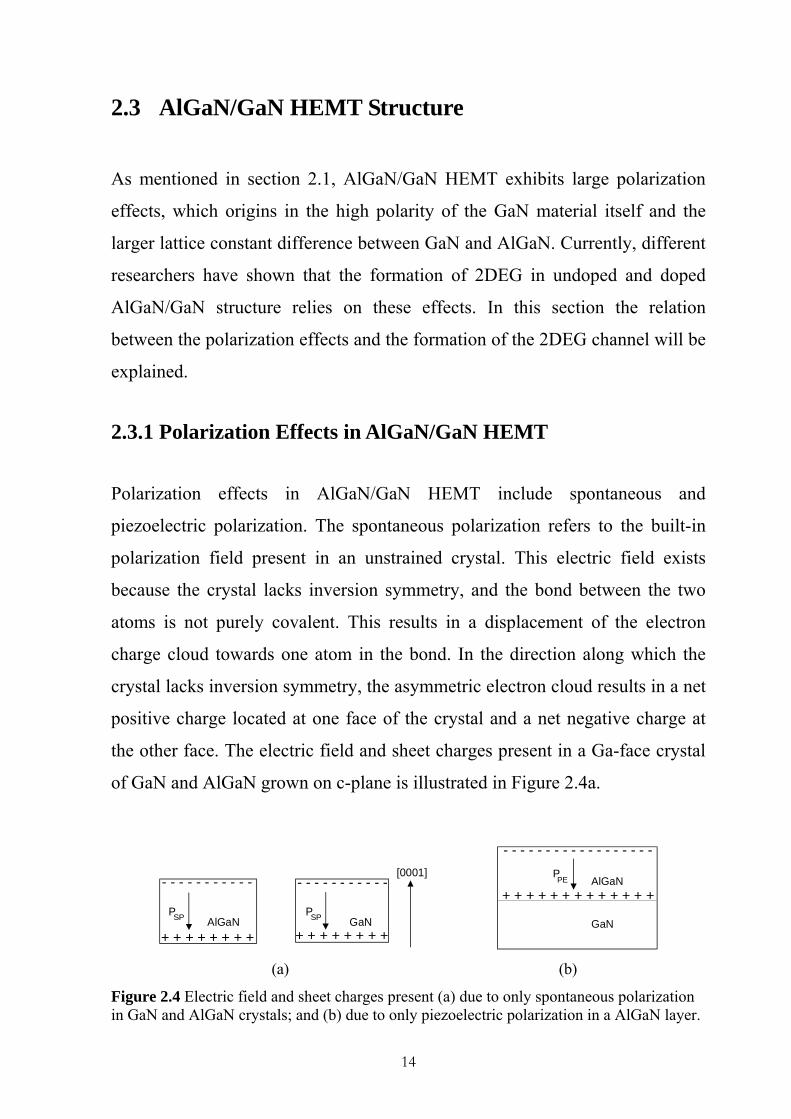
2.4 Electric field and sheet charges present (a) due to only spontaneous
polarization in GaN and AlGaN crystals; and (b) due to only
piezoelectric polarization in a AlGaN layer……………...………….. 14
2.5 Combined piezoelectric and spontaneous polarization field in
AlGaN/GaN structure……………………………………………….. 15
2.6 AlGaN/GaN HEMT structure showing polarization induced, surface
states, and 2DEG charges…………………………………………… 16
2.7 Epitaxial layer structure of the AlGaN/GaN HEMT [13]…………… 18
2.8 (a) Bad pinch-off DC characteristics, measured in house, of a 8x125 µm
gate width AlGaN/GaN HEMT (wafer no. 713-2) related to the buffer
leakage current, (b) kink effect in DC characteristics, measured in FBH,
of a 8x125 µm gate width AlGaN/GaN HEMT (wafer no. 713-2) related
to the buffer traps……………………………………………………. 20
VIII

2.9 DC IV characteristics of a 8x125 µm gate width AlGaN/GaN HEMT
(wafer no. 398-4) measured in IAF ……………………………… 22
2.10 Measured pulsed IV, in IAF, in comparison with DC IV characteristics
for 8x125 µm gate width AlGaN/GaN HEMT (wafer no. 398-4) at: (a)
VDSO = 25 V and VGSO = -4 V and (b) at VDSO = 0 V and VGSO = -7 V
quiescent bias voltages……………………………………………… 23
2.11 Measured pulsed IV, in IAF and FBH, in comparison with DC IV
characteristics for 8x125 µm gate width AlGaN/GaN HEMT on
two different wafers at: VDSO = 25 V and VGSO ≈ Vpinch-off
quiescent bias voltages………………………………………………. 23
2.12 Measured unity gain frequency (ft) and maximum oscillation frequency
(fmax) versus gate voltage for a 8x125 µm gate width AlGaN/GaN
HEMT (wafer no. 713-2) at different drain voltages…………..…….. 25
2.13 Single-tone power sweep in-house measurements for class AB (IDS =
0.2IDSS) operated 8x125 µm gate width AlGaN/GaN HEMT on two
different wafers at 2 GHz in a 50 Ω source and load environment…. 25
3.1 Intrinsic quasi-static small-signal equivalent circuit model [31]…… 33
3.2 Quasi-static large-signal model…………………………………….. 34
3.3 Intrinsic non-quasi-static linear device equivalent circuit………….. 35
3.4 Non-quasi-static large-signal model………………………………… 36
3.5 Non-quasi-static large-signal model including trapping induced
dispersion…………………………………………………………….. 39
3.6 Equivalent circuit implementation for device self-heating process….. 41
IX

4.1 22-element distributed model for active AlGaN/GaN HEMT……….. 53
4.2 Gate-drain and gate-source capacitances estimation from different
measured data ranges for a 0.5 µm AlGaN/GaN HEMT with
a 2x50 µm gate width (wafer no. 398-4)…………………………….. 54
4.3 Flowchart of the model parameter starting value generation
algorithm…………………………………………………………….. 56
4.3 (continued).……....………………………………………………….. 57
4.4 Cold pinch-off equivalent circuit for the AlGaN/GaN HEMT at low
frequency…………………………………………………………….. 58
4.5 T-network representation of a cold pinch-off equivalent circuit for
the AlGaN/GaN HEMT…………………………………………….. 59
4.6 Inductance estimation from the cold pinched-off stripped
Z-parameters for a 0.5 µm AlGaN/GaN HEMT with
a 2x50 µm gate width (wafer no. 398-4)…………………………… 60
4.7 Residual error between measured and simulated S-parameters versus
Cpga and Cgda for a 0.5 µm AlGaN/GaN HEMT with a 2x50 µm
gate width (wafer no. 398-4)……………………………………….. 61
4.8 Resistance estimation from the cold forward stripped Z-parameters
for a 0.5 µm AlGaN/GaN HEMT with a 2x50 µm gate width
(wafer no. 398-4)…………………………………………………… 63
4.9 Pinchoff S-parameter fitting with starting element values for the 22-
element equivalent circuit model of a 0.5 µm AlGaN/GaN HEMT
with a 2x50 µm gate width (wafer no. 398-4)……………..……….. 63
X

4.10 Extracted intrinsic capacitances and conductances versus frequency
at VGS = -1 V and VDS = 10 V for a 0.5 µm AlGaN/GaN HEMT with a
2x50 µm gate width (wafer no. 398-4)…………………….……… 68
4.11 Fitting of the highly correlated measured data of a 0.5-µm
AlGaN/GaN HEMT with a 2 x 50 µm gate width (wafer no. 398-4)
at VGS = -2.0 V, VDS =20 V for extraction Cgs and Ri……………… 69
4.12 Extracted Cgs, Cgd, Gm, and Gds as a function of the extrinsic
voltages for a 0.5 µm AlGaN/GaN HEMT with a 2x50 µm
gate width (wafer no. 398-4)……………………………………….. 70
4.13 Extracted Ri, τ, Ggsf, and Ggdf as a function of the extrinsic voltages
for a 0.5 µm AlGaN/GaN HEMT with a 2x50 µm gate width
(wafer no. 398-4)…………………………………………………… 70
4.14 Extracted Rgd and Cds as a function of the extrinsic voltages for a
0.5 µm AlGaN/GaN HEMT with a 2x50 µm gate width
(wafer no. 398-4)…………………………………………………… 71
4.15 Comparison of measured data from IAF for a 0.5 µm AlGaN/GaN
HEMT with a 2x50 µm gate width on wafer no. 398-4 (circles)
with simulation results (lines)………………………………………. 74
4.16 Errors between simulated and measured S-parameters for a 0.5-µm
AlGaN/GaN HEMT with a 2x50 µm gate width (wafer no. 398-4)… 74
4.17 Variation of the calculated intrinsic transient frequency with the
extrinsic bias voltages for a 0.5 µm AlGaN/GaN HEMT with
a 2x50 µm gate width (wafer no. 398-4)…………………………… 75
XI

4.18 Variation of the calculated effective gate length with the extrinsic
bias voltages for a 0.5-µm AlGaN/GaN HEMT with a 2x50 µm gate
width (wafer no. 398-4)……………………………………………. 76
4.19 Pinch-off S-parameter measurements from IAF for 16x250 µm and
8x125 µm gate width AlGaN/GaN HEMTs (wafer no. 707-4)…….. 77
4.20 Optimal frequency range for reliable model parameter extraction…. 78
4.21 Comparison of measured data from IAF for a 8x125 µm
AlGaN/GaN HEMT on wafer no. 707-4 (circles) with
simulation results (lines)……….…………………………………… 81
4.22 Comparison of measured data from IAF for a 8x250 µm
AlGaN/GaN HEMT on wafer no. 707-4 (circles) with
simulation results (lines)……………………………………………. 81
4.23 Comparison of measured data from IAF for a 16x250 µm
AlGaN/GaN HEMT on wafer no. 707-4 (circles) with
simulation results (lines)……………………………………………. 82
5.1 Large-signal model for AlGaN/GaN HEMT including self-heating
and trapping effects…………………………………………………. 85
5.2 Simulated normalized transconductance and output conductance
for a 8x125 µm AlGaN/GaN HEMT (wafer no. 713-2) at
VDS = 24 V and VGS = -2 V………………………………………… 86
5.3 Extracted intrinsic gate capacitance and channel transconductance
and their higher derivatives at Vds = 10 V for a 8x125 µm gate
width AlGaN/GaN HEMT (wafer no. 713-2)……………………… 87
XII

5.4 Calculated gate charge sources Qgs and Qgd versus intrinsic voltages
for a 8x125 µm gate width AlGaN/GaN HEMT (wafer no. 713-2)… 88
5.5 Calculated gate current sources Igs and Igd versus intrinsic voltages
for a 8x125 µm gate width AlGaN/GaN HEMT (wafer no. 713-2)… 89
5.6 FBH pulsed IV measurements for a 8x125 µm gate width
AlGaN/GaN HEMT (wafer no. 713-2) at: (a) zero quiescent drain
voltage to characterize the surface trapping; and (b) below the
pinch-off quiescent gate voltage to characterize the buffer trapping… 91
5.7 FBH pulsed IV measurements for a 8x125 µm gate width
AlGaN/GaN HEMT (wafer no. 713-2) at high quiescent dissipated
power in comparison with zero quiescent dissipated power
characteristics to characterize the HEMT self-heating……………… 91
5.8 Bias-dependent trapping fitting parameters of the drain current
model in (5.3) extracted from the pulsed IV measurements of
a 8x125 µm AlGaN/GaN HEMT (wafer no. 713-2)……………….. 92
5.9 Extracted isothermal DC drain current (a) and bias-dependent self-
heating fitting parameter (b) for a 8x125 µm AlGaN/GaN HEMT
(wafer no. 713-2)…………………………………………………… 93
5.10 Large-signal model implementation in ADS (Advances Design
System) software…………………………………………………… 94
5.11 Simulated (lines) and measured (circles) S-parameters by UNIK
of a 8x125 µm AlGaN/GaN HEMT (wafer no. 713-2) at
VGS = -2.0 V and VDS = 9.0 V……………………………….……... 96
XIII

5.12 Comparison of measured (circles) and simulated (lines) S-parameter for
a 8x125-µm AlGaN/GaN HEMT on wafer no. 398-4 at VGS = -3.0 V and
VDS = 21.0 V ……………………………………………………… 96
5.13 Pulsed IV simulations (lines) and FBH measurements (circles) for a
8x125 µm AlGaN/GaN HEMT (wafer no. 713-2) at different quiescent
bias conditions……………………………………………………. 97
5.14 Simulated (lines) and measured (symbols) large-signal waveforms
by IAF for class AB operated 8x125-µm AlGaN/GaN HEMT
(wafer no. 398-4) at 16 dBm input power………………………… 98
5.15 Single-tone power sweep simulations (lines) and UNIK
measurements (symbols) for class A operated 8x125 µm
AlGaN/GaN HEMT (wafer no. 713-2) at 2 GHz in a
50 Ω source and load environment……….……………………….. 99
5.16 Single-tone power sweep simulations (lines) and IAF
measurements (symbols) for class AB operated 8x125 µm
AlGaN/GaN HEMT (wafer no. 398-4) at 2 GHz in a
50 Ω source and load environment……….……………………….. 99
5.17 Simulated (lines) and UNIK measured (symbols) output and input
powers per tone under two-tone excitation centered at 2 GHz and
separated by 100 kHz for class A operated 8x125 µm AlGaN/GaN
HEMT (wafer no. 389-4) in a 50 Ω source and load environment… 100
5.18 Simulated (lines) and UNIK measured (symbols) output and input
powers per tone under two-tone excitation centered at 2 GHz and
separated by 100 kHz for class AB operated 8x125 µm AlGaN/GaN
HEMT (wafer no. 713-2) in a 50 Ω source and load environment… 100
XIV

5.19 Simulated lower intermodulation distortion and carrier to intermod-
ulation ratio versus input power per tone under two-tone excitation
centered at 2 GHz and separated by 100 kHz for a 8x125 µm
AlGaN/GaN HEMT (wafer no. 713-2) under 20V drain bias voltage
for different gate bias voltages in a 50Ω source and load
environment………………………………………………………… 101
XV

List of Tables
2.1 Table of properties of Si, GaAs and GaN [8]……………………….. 13
4.1 Starting values for 22-element equivalent circuit model of a 0.5 µm
AlGaN/GaN HEMT with a 2x50 µm gate width (wafer no. 398-4)… 64
4.2 Optimized pinch-off device parameters of a 0.5 µm AlGaN/GaN
HEMT with a 2x50 µm gate width (wafer no. 398-4).……………… 67
4.3 Extracted model parameters for different device sizes
(wafer no. 707-4)……………………………………………………. 79
4.4 Intrinsic model parameters at VGS = -2V and VDS = 21V for different
device sizes (wafer no. 707-4)………………………………………. 80
XVI

List of Symbols
ns sheet carrier density cm-2
Eg bandgap energy eV
Ebr breakdown electric field V/cm
Vbreakdown breakdown voltage V
vs electron saturation velocity cm/s
q electron charge (1.6 ⋅ 10-19) coulomb
ft extrinsic unity gain frequency Hz
fT intrinsic unity gain frequency Hz
fmax extrinsic maximum oscillation frequency Hz
Leff effective gate length µm
µ electron mobility cm2/Vs
E electric field V/cm
LG gate length µm
h21 short circuit current gain dB
Gm intrinsic channel transconductance S
GM extrinsic channel transconductance S
τ transit delay time s
Gds intrinsic channel conductance S
GDS extrinsic channel conductance S
Ggsf gate forward conductance S
Ggdf gate breakdown conductance S
Rgd intrinsic gate-drain charging resistance Ω
Ri intrinsic gate-source charging resistance Ω
Cds intrinsic drain-source capacitance F
Vds intrinsic drain-source voltage V
Vgs intrinsic gate-source voltage V
XVII

VDS extrinsic drain-source voltage V
VGS extrinsic gate-source voltage V
Ids intrinsic drain-source current A
Rth thermal resistance oC/W
Cth thermal capacitance sW/oC
IV current-voltage
Cpga gate-source pad capacitance F
Cpda drain-source pad capacitance F
Cgda gate-drain pad capacitance F
Lg gate metallisation inductance H
Ld drain metallisation inductance H
Ls source metallisation inductance H
Cpgi gate-source interelectrode capacitance F
Cpdi drain-source interelectrode capacitance F
Cgdi gate-drain interelectrode capacitance F
Rg gate parasitic resistance Ω
Rd drain parasitic resistance Ω
RS source parasitic resistance Ω
Vp pinch-off gate-source voltage V
ω angular frequency rad/s
K stability factor
G active device gain dB
T absolute temperature K
∆T internal temperature raise K
Pdiss instantaneous power dissipation W
Pdisso average power dissipation W
S small-signal scattering parameter
Z small-signal impedance parameter Ω
XVIII

Y small-signal admittance parameter S
Igs intrinsic gate-source current A
Igd intrinsic gate-drain current A
Qg intrinsic gate charge coulomb
Qd intrinsic drain charge coulomb
Qgs intrinsic gate-source charge coulomb
Qgd intrinsic gate-drain charge coulomb
αG surface trapping fitting parameter
αD buffer trapping fitting parameter
αT thermal fitting parameter DC
isodsI , isothermal intrinsic DC drain current A
Pout RF output power W
Pin RF input power W
XIX

List of Abbreviations And Acronyms
3G third generation
RF radio frequency
PA RF power amplifier
AC alternating current
DC direct current
dB decibel (W)
dBm decibel (mW)
HEMT high electron mobility transistor
FET field effect transistor
MESFET metal-semiconductor FET
IMD intermodulation distortion
IMD3 third order intermodulation distortion
IMR intermodulation distortion ratio
2DEG two-dimensional electron gas
PAE power added efficiency
JFOM Johnson figure of merit
BFOM Baliga figure of merit
MOCVD metal organic chemical vapour deposition
TLM thermal lens microscope
FBH Ferdinand-Braun Institut für Höchstfrequenztechnik
IAF Fraunhofer Institute for Applied Solid-State Physics
UPG Mason’s unilateral power gain
AAN artificial neural network
ADS® advanced design system
SDD symbolically defined device
DAC data access component
XX

Abstract
Nowadays, microwave technology is critical in the areas of high RF power for
microwave radar and communication transmitter applications. In these
applications, microwave device is adopted to produce high RF power levels at
high frequency and to operate at high temperature for designing the front-end
high power amplifier (HPA) of the transmitter. In addition to the high RF
output power, power added efficiency (PAE) and linearity should be optimized
to meet the requirements of the high capacity and high quality services of next
generation communication systems. Therefore, most favorable device and
improved design for the HPA is strongly demanded.
AlGaN/GaN HEMT technology is becoming an interesting candidate for
the HPA design. Since GaN is a wide band gap material, GaN-based device
will have inherent high breakdown voltage; and therefore can operate at higher
bias voltage and higher RF power level. Also due to its high saturation
velocity, the device will have a high operating frequency. Another advantage of
the device is the high operating temperature, which attributed to the lower
thermal resistance of GaN and the excellent thermal properties of the employed
SiC substrate. However, the main obstacle, which still limits the RF output
power of the device, is the self-heating and trapping induced current dispersion.
Large-signal model for AlGaN/GaN HEMT, which can simulate the
output power, PAE, and nonlinear behavior of the device, is very crucial for the
HPA design. This is the main problem, which is addressed by this thesis. The
proposed solution is implemented into two steps. The first step is developing a
small-signal modeling approach, which can accurately describe the parasitic
elements and the bias dependent intrinsic part of the device. The second step is
deriving a large-signal model from the developed small-signal one in a bottom-
up constructive manner.
XXI

In the first part of the thesis, the developed small-signal modeling
approach for AlGaN/GaN HEMT is presented. In this approach, a new method
for extracting the parasitic elements of the device is developed. This method is
based on two steps, which are: 1) generation of high-quality starting values for
the extrinsic parameters that would place the extraction close to the global
minimum of the objective function for a distributed equivalent circuit model
and 2) searching for the optimal model parameter values through optimization
using the starting values already obtained. The bias-dependent intrinsic
parameter extraction procedure is improved for optimal extraction. The validity
of the developed modeling approach and the proposed small-signal model is
demonstrated through simulated and measured S-parameters for different
device sizes up to 4-mm gate width.
In the second part of the thesis, a table-based large-signal model for
AlGaN/GaN HEMT accounting for trapping and self-heating induced current
dispersion is presented. The model elements construction is optimized in terms
of the device nonlinearity prediction. The model implementation takes into
account the dynamic behavior of the trapping and self-heating phenomena. The
model validity is verified through simulated and measured outputs of the
device under pulsed and continuous large-signal excitations for 1-mm gate
width devices. Single- and two-tone simulation results show that the model can
efficiently predict the output power and its harmonics and the associated
intermodulation distortion under different input power and bias conditions.
XXII

Zusammenfassung
Heutzutage steht die Mikrowellentechnologie auf dem Gebiet hoher HF-
Leistungen für Mikrowellenradar- und Kommunikationsanwendungen vor
neuen Herausforderungen. In dem genannten Anwendungsbereich soll der
Mikrowellentransistor beim Entwurf der erforderlichen
Hochleistungsverstärker (HPA) in der Lage sein, Hochleistungssignale zu
produzieren. Er soll insbesondere auch bei hohen Temperaturen arbeiten
können. Dabei soll die Linearität und die Effizienz (PAE) der
Hochleistungssignale optimiert werden, um den höheren Kanalkapazitäts- und
Qualitätsanforderungen der nächsten Generation der Kommunikationssysteme
gerecht zu werden. Aufgrund dieser Forderung soll ein neuer
Mikrowellentransistor entwickelt werden.
AlGaN/GaN HEMT Technologie ist für den Entwurf von HPAs geeignet,
da der GaN Transistor aus einem Material mit großer Bandlücke besteht, was
zu einer hohen Sperrspannung führt. Somit kann er mit einer höheren
Betriebsspannung und Hochleistungssignalen arbeiten. Der GaN Transistor
kann wegen seiner hohen Sättigungsdriftgeschwindigkeit bei höheren
Arbeitsfrequenzen betrieben werden. Ein weiterer Vorteil des Bauelements ist
die hohe Betriebstemperatur, die dem niedrigen thermischen Widerstand von
GaN und den ausgezeichneten thermischen Eigenschaften des eingesetzten SiC
Substrates zugeschrieben wird. Jedoch ist das Haupthindernis, das die RF
Ausgangsleistung des Bauelements begrenzt, die Frequenzdispersion, die von
Selbsterwärmung und Störstellen verursacht wird.
Das Großsignalmodell für ein AlGaN/GaN HEMT, das die
Ausgangsleistung, die PAE und das nichtlineare Verhalten des Bauelements
simulieren kann, ist für den Entwurf von HPA sehr entscheidend. Dies ist das
Hauptproblem, welches in der vorliegenden Arbeit behandelt wird. Im ersten
XXIII

Schritt wird ein Kleinsignalmodellierungsansatz entwickelt. Er kann die
parasitären Elemente und die arbeitspunktabhängigen intrinsischen Teile der
Bauelemente genau analysieren. Im zweiten Schritt wird vom
Kleinsignalmodell ein Großsignalmodell in einer konstruktiven “bottom-up”
Weise hergeleitet.
Im ersten Teil der Arbeit wird der entwickelte Kleinsignalmodellierungs-
ansatz für einem AlGaN/GaN HEMT dargestellt. In diesem Ansatz wird eine
neue Methode für die Extraktion der parasitären Eigenschaften des
Bauelements entwickelt. Diese Methode basiert auf zwei Schritten: Zuerst
werden mit Hilfe von kalten S-Parameter-Messungen, hochwertige
Anfangswerte für die extrinsischen Parameter erzeugt. Diese Werte sind nah an
dem globalen Minimum der Zielfunktion für ein verteiltes Kleinsignalmodell.
Danach werden mit den bereits erhaltenen Anfangswerten die optimalen
Modellparameterwerte gesucht. Das intrinsische Parameter-Extraktions-
verfahren wurde entwickelt, damit es optimale Werte liefern kann. Die
Gültigkeit des entwickelten Modellierungsansatzes und des vorgeschlagenen
Kleinsignalmodells wird durch Simulationen und Messung der S-Parameter für
unterschiedliche Größen von Bauelementen bis 4-mm Gate-Länge verifiziert.
Im zweiten Teil der Arbeit, wird ein genaues Großsignalmodell für einen
AlGaN/GaN HEMT entwickelt. Dieses Modell behandelt die Frequenz-
dispersion, die von Selbsterwärmung und Störstellen verursacht wird. Dieses
Modell kann nicht nur die Nichtlinearität von GaN Transistoren simulieren,
sondern auch das dynamische Verhalten der Selbsterwärmung und Störstellen-
phänomene. Die Modellgültigkeit wird durch Simulationen und Ergebnisse aus
Messungen unter gepulster und kontinuierlicher Großsignalanregung für
Bauelemente mit 1-mm Gate-Länge überprüft. Die Ergebnisse der Ein- und
Zweiton-Simulationen zeigen, daß dieses Modell effizient die
Ausgangsleistung mit seinen Harmonischen und die
XXIV

Intermodulationsverzerrung bei unterschiedlichen Eingangsleistungen und
Betriebsspannungen voraussagen kann.
XXV

Chapter 1
Introduction
Third generation (3G) high data rate wireless communication systems are
planned to offer new ways to access information and services with higher data
speed and data bandwidth [1]. This requires increase of capacity of the current
systems to provide not only voice service but also data delivery. Also in the
infrastructure of these systems, several crucial hardware components should be
improved to meet the quality service of the 3G systems. Among these
components, RF power amplifiers (PAs) are considered the most challenging
area. In order to provide sufficient quality of service for high user capacity, one
will need highly linear PAs with high power efficiency [2], [3].
PAs linearity can be improved either by adding external circuits, or simply
by improving those design. However, since the first technique involves several
drawbacks like cost, size, effective bandwidth or difficulty of adjustment, there
is a growing interest in direct optimization of the actual PA linearity in terms of
the employed active device [4]. Leakage currents in the active device, which
are almost technology dependent, are the main factors that influence the power
efficiency of the constructed PA [5], [6]. Therefore, an improved device
technology is needed for designing PAs for the 3G communication systems.
AlGaN/GaN HEMT is an excellent candidate for fabrication of 3G PAs. It
has high sheet carrier density and high saturation electron velocity, which
produce high output power. Also it has high electron mobility, which is largely
responsible for low on-resistance, and therefore, high power added efficiency
1

could be achieved. As a result of its wideband material, AlGaN/GaN HEMT
can achieve very high breakdown voltage, very high current density, and
sustain very high channel operating temperature. All of these factors indirectly
improve the linearity of the AlGaN/GaN HEMT [7]. Furthermore, possible
epitaxial growth on silicon carbide substrate, which has excellent thermal
properties, makes this device optimal for high-power RF application.
AlGaN/GaN HEMT is still under development and there is no commercial
product currently available for this device. The past decade has seen rapid
progress toward the development of AlGaN/GaN HEMT with a focus on their
power performance [8]-[13]. However, despite the high output power of this
device, current dispersion is the biggest obstacle to obtain reproducible power
performance [14]-[19]. Even for AlGaN/GaN HEMT on high thermal
conductivity SiC substrates, a device temperature increase can be observed
from the output characteristics [20].
The design of PAs for the 3G communication systems based on
AlGaN/GaN HEMT requires an accurate large-signal model for this device.
This model should account for current dispersion and temperature dependent
performance in addition to other high-power stimulated effects like gate
forward and gate breakdown. Also the model should be able to predict
intermodulation distortion (IMD), which is very important for PAs nonlinearity
analysis. To the knowledge of the author, there is no efficient large-signal
model for AlGaN/GaN HEMT available, which describes all these effects. The
analytical models reported in [21]-[23] con simulate the fundamental output
power including the current dispersion and thermal characteristics of the
AlGaN/GaN HEMT. However, these models have poor IMD prediction
capabilities. In another reported model [24] no IMD simulation has been
presented. The model presented in [25] has been optimized for IMD
simulation, but it does not account for the current dispersion or the temperature
dependent characteristics. The main aim of this research is to develop a large-
2

signal model for AlGaN/GaN HEMT, which can simulate all of the mentioned
effects in an efficient manner.
The Department of High Frequency Engineering has been involved in the
topic of active device modeling for more than fifteen years now, especially for
GaAs-based devices. The work reported in this thesis is aimed at extending the
techniques developed, and to apply it to the modeling of the AlGaN/GaN
HEMT. The first work in the department was on the topic of model parameter
extraction reported by Schlechtweg [26]. Schlechtweg developed a calibration
technique for microstrip test-fixtures and employed it to the characterization of
MESFETs and HEMTs based on error-corrected small-signal S-parameter
measurements up to 40 GHz. Based on the calibration procedure developed by
Schlechtweg, van Raay [27] developed a large-signal characterization
technique based on active load-pull technique and employed it to direct
extraction of large-signal model parameters from signal waveform using a
numerical harmonic-balance technique. Lin [28] and Kompa and Novotny [29]
then extended the parameter extraction method and Werthof [30] enhanced the
direct parameter extraction from large-signal measurements. Based on the
observation that small-signal model is a linearization of the large-signal one,
Schmale in [31] proposed a top-down modeling approach. Hence, consistent
small-signal model can be derived from the corresponding large-signal model
in a hierarchical top-down manner. However, the derived small-signal model
topology may not match the structure of the device. Therefore, another
modeling approach, which followed by Mwema [32], started from physics-
relevance distributed small-signal equivalent circuit model to derive a large-
signal model in constructive bottom-up manner. For this purpose, an
optimisation-based method for reliable extraction of the small-signal model
parameters was developed. In this extraction method, an algorithm with
automatic generation of starting values was developed instead of using the
previous user intervention method proposed by Lin and Kompa [28], [33] and
3

Novotny and Kompa [34], [35]. Based on the starting values generated from
cold pinch-off measurements, all extrinsic parameters for the small-signal
model have become determined.
The reliability of the generated starting values depends on the quality of
the measurements, which suffer from non-avoidable measurement uncertainty
[34], [36], [37]. The amount of this uncertainty increases as the active device is
biased near the pinch-off [38]. Therefore, it can be difficult to determine
reliable starting values for all the model elements using only pinch-off
measurements. Under the assumption of small gate and drain extrinsic
resistances, Mwema reduced the number of the model elements by
incorporating the outer and interelectrode gate-drain parasitic capacitances with
the intrinsic gate-drain capacitance. This assumption may be valid for
AlGaAs/GaAs devices but does not hold for AlGaN/GaN HEMT, which has
higher contact resistances [39], [40]. Also the model does not consider the gate-
forward and gate-breakdown effects, which are very important to account for
high power devices like AlGaN/GaN HEMT.
Thus, the initial aim of the current work described in this thesis was to
extend the small-signal equivalent circuit model by including the gate-drain
parasitic capacitances. Also modifying the extraction procedure by including a
forward measurement in addition to the pinch-off one to generate reliable
starting values for the model elements. The intrinsic part of the equivalent
circuit model was also extended to account for the gate-forward and gate-
breakdown effects. The extended small-signal model is the basis of the
AlGaN/GaN HEMT large-signal modeling, which is the main aim of this
research. To achieve this aim, a table-based large-signal model for AlGaN/GaN
HEMT accounting for trapping and self-heating induced current dispersion was
developed. However, since the model capability of nonlinearity prediction is
correlated with the quality of the model elements data with respect to intrinsic
voltages [41], spline approximation technique [42] was used to construct these
4

data. This technique can maintain the continuity of the data and its higher order
derivatives and therefore improve the harmonics and intermodulation
distortions simulations [43], [44]. Also the model was implemented in such a
way to take into account the dynamic behavior of trapping and self-heating
phenomena, which improve the model capability for memory effect analysis
[45], [46].
This thesis is sectioned as follows: Chapter 1 describes the objective of
the thesis and the motivation behind performing this research. The history of
the active device modeling work in the Department of High Frequency
Engineering is also described here in relation with the topic handled in the
thesis. In Chapter 2, a brief description of the fundamentals of physics and
operation of AlGaN/GaN HEMT is given in order to provide the physical
origin of the main behaviors to be modeled. Fundamental principles of the
active device modeling are presented in Chapter 3 to give an overview about
the general modeling approaches and those advantages and disadvantages. The
bottom-up modeling approach, which is followed in this work, was also
described in addition to methods of modeling of the current dispersion. The
developed small-signal modeling approach for AlGaN/GaN HEMT is
presented in Chapter 4. The extraction procedure of the small-signal model
parameters is described and the modeling accuracy and the reliability of
extraction results are verified. The validity of this modeling approach for larger
AlGaN/GaN HEMTs is also investigated. The developed large-signal model for
AlGaN/GaN HEMT is presented in Chapter 5. The model equivalent circuit in
addition to the model element extraction procedure is explained. And then, the
model implementation and verification by comparison of small- and large-
signal simulations with measurements are presented. Conclusions and
recommendation for further work are then finally drawn and presented in
Chapter 6.
5

References
[1] M. Feng, S.-C. Shen, D. C. Caruth, and J.-J. Huang, “Device technologies for RF front-end circuits in next-generation wireless communications,” Proceeding of the IEEE, vol. 92, pp. 354-375, February 2004.
[2] H. Ku and J. S. Kenney, “Behavioral modeling of nonlinear RF power amplifiers considering memory effects,” IEEE Trans. Microw. Theory Tech., vol. 51, pp. 2495-2504, December 2003.
[3] R. Raich and G. T. Zhou, “On the modeling of memory nonlinear effects of power amplifiers for communication applications,” 10th IEEE DSP Workshop Proc., GA, pp. 7-10, October 2002.
[4] P. M. Cabral, N. B. Carvalho and J. C. Pedro, “An integrated view of nonlinear distortion phenomena in various power amplifier technologies,” 11th GAAS Symposium, pp. 69-72, Munich, October 2003.
[5] Y. B. Martynov, E. V. Pogorelova, and Y. V. Buvaylik, “Investigation of physical mechanisms limiting maximum output power and efficiency of MESFETs,” International Crimean Conference: Microwave & Telecommunication Technology, Sevastopol, Ukraine, pp. 212-213, September 2003.
[6] W. Saito, M. Kuraguchi, Y. Takada, K. Tsuda, I. Omura, and T. Ogura, “Influence of surface defect charge at AlGaN-GaN-HEMT upon Schottky gate leakage current and breakdown voltage,” IEEE Trans. on Electron Devices, vol. 52, pp. 159-164, February 2005.
[7] M. A. Khan, G. Simin, J. Yang, J. Zhang, A. Koudymov, M. S. Shur, R. Gaska, X. Hu, and A. Tarakji, “Insulating gate III-N heterostructure field-effect transistors for high-power microwave and switching applications,” IEEE Trans. on Electron Devices, vol. 51, pp. 624-633, February 2003.
[8] Y. Ando, Y. Okamoto, H. Miyamoto, T. Nakayama, T. Inoue, and M. Kuzuhara, “10-W/mm AlGaN-GaN HFET with a field modulating plate,” IEEE Electron Device Lett., vol. 24, pp. 289-291, May 2003.
[9] S. T. Sheppard, K. Doverspike, W. L. Pribble, S. T. Allen, J. W. Palmour, L. T. Kehias, and T. J. Jenkins, “High-power microwave GaN/AlGaN HEMTs on semi-insulating silicon carbide substrates,” IEEE Electron Device Lett., vol. 20, pp. 161-163, April 1999.
[10] L. F. Eastman, V. Tilak, J. Smart, B. M. Green, E. M. Chumbes, R. Dimitrov, K. Hyungtak, O. S. Ambacher, N. Weimann, T. Prunty, M. Murphy, W. J. Schaff, and J. R. Shealy, “Undoped AlGaN/GaN HEMTs for microwave power amplification,” IEEE Trans. on Electron Devices, vol. 48, pp. 479-485, March 2001.
[11] J. Shealy, V. Kaper, V. Tilak, T. Prunty, A. Smart, B. Green, and L. Eastman, “An AlGaN/GaN high-electron-mobility transistor with an AlN sub-buffer layer,” J. Phy. Condensed Matter, vol. 14, pp. 3499-3509, April 2002.
6
[12] J. S. Moon, M. Micovic, P. Janke, P. Hashimoto, W.-S. Wong, R. D. Widman, L. McCray, A. Kurdoghlian, and C. Nguyen, “GaN/AlGaN HEMTs operating at 20 GHz with continuous-wave power density > 6W/mm,” Electron. Lett., vol. 37, pp. 528-530, April 2001.
[13] Y.-F. Wu, A. Saxler, M. Moore, R. P. Smith, S. Sheppard, P. M. Chavarkar, T. Wisleder, U. K. Mishra, and P. Parikh, “30-W/mm GaN HEMTs by field plate optimization,” IEEE Electron Device Lett., vol. 25, pp. 117-119, March 2004.
[14] R. Vetury, N. Q. Zhang, S. Keller, and U. K. Mishra, “The impact of surface states on the DC and RF characteristics of AlGaN/GaN HFETs,” IEEE Trans. on Electron Devices, vol. 48, pp. 560-566, March 2001.
[15] G. Meneghesso, G. Verzellesi, R. Pierobon, F. Rampazzo, A. Chini, U. K. Mishra, C. Canali, and E. Zanoni, “Surface-related drain current dispersion effects in AlGaN-GaN HEMTs,” IEEE Trans. Microw. Theory Tech., vol. 51, pp. 1554-1561, October 2004.
[16] S. C. Binari, K. Ikossi, J. A. Roussos, W. Kruppa, D. Park, H. B. Dietrich, D. D. Koleske, A. E. Wickenden, and R. L. Henry, “ Trapping effect and microwave power performance in AlGaN/GaN HEMTs,” IEEE Trans. on Electron Devices, vol. 48, pp. 465-471, March 2001.
[17] S. Nuttinck, S. Pinel, E. Gebara, J. Laskar, and M. Harris,“ Cryogenic investigation of current collapse in AlGaN/GaN HFETS,” 11th GAAS Symposium, Munich, pp. 213-215, October 2003.
[18] T. Mizutani, Y. Ohno, M. Akita, S. Kishimoto, and K. Maezawa, “A study on current collapse in AlGaN/GaN HEMTs induced by bias stress,” IEEE Trans. on Electron Devices, vol. 50, pp. 2015-2020, October 2003.
[19] I. Daumiller, D. Theron, C. Gaquiere, A. Vescan, R. Dietrich, A. Wieszt, H. Leier, R. Vetury, U. K. Mishra, I. P. Smorchkova, S. Keller, N. X. Nguyen, C. Nguyen, and E. Kohn, “Current instabilities in GaN-based devices,” IEEE Electron Device Lett., vol. 22, pp. 62-64, February 2001.
[20] R. Gaska, Q. Chen, J. Yang, A. Osinsky, M. Asif Khan, and M. S. Shur, “High-temperature performance of AlGaN/GaN HFETs on SiC substrates,” IEEE Electron Device Lett., vol. 18, pp. 492–494, October 1997.
[21] B. M. Green, K. K. Hyungtak Kim Chu, H. S. Lin, V. Tilak, J. R. Shealy, A. J. Smart, and L. F. Eastman, “Validation of an analytical large signal model for AlGaN/GaN HEMTs,” MTT-S International Microwave Symposium Dig., Boston, MA, pp. 761-764, June 2000.
[22] J.-W. Lee, S. Lee, and K. J. Webb, “Scalable large-signal device model for high power-density AlGaN/GaN HEMTs on SiC,” MTT-S International Microwave Symposium Dig., Phoenix, AZ, pp. 679-682, May 2001.
[23] J.-W. Lee and K. J. Webb, “A temperature-dependent nonlinear analytic model for AlGaN-GaN HEMTs on SiC,” IEEE Trans. Microw. Theory Tech., vol. 52, pp. 2-9, January 2004.
7

[24] F. van Raay, R. Quay, R. Kiefer, M. Schlechtweg, and G. Weimann, “ Large signal modeling of AlGaN/GaN HEMTs with Psat > 4 W/mm at 30 GHz suitable for broadband power applications,” MTT-S International Microwave Symposium Dig., Philadelphia, PA, pp. 451-454, June 2003.
[25] P. M. Cabral, J. C. Pedro, and N. B. Carvalho, “Nonlinear device model of microwave power GaN HEMTs for high power-amplifier design,” IEEE Trans. Microw. Theory Tech., vol. 52, pp. 2585-2592, November 2004.
[26] M. Schlechtweg, “Breitbandige Charakterisierung und Modellierung von GaAs-MESFETs und (AlGa)As/GaAs-MODFETs bis 40 GHz,” Doctoral Thesis (in German), Department of High Frequency Engineering, University of Kassel, Kassel, Germany, 1989.
[27] F. van Raay, “Fehlerkorrigiertes 20 GHz-Signalformmeßsystem zur direkten Großsignalanalyse von Mikrowellen-Feldeffekttransistoren,” Doctoral Thesis (in German), Department of High Frequency Engineering, University of Kassel, Kassel, Germany, 1990.
[28] F. Lin, “Ein Verfahren zur zuverläsigen experimentellen Modellierung von Mikrowellen-FETs,” Doctoral Thesis (in German), Department of High Frequency Engineering, University of Kassel, Kassel, Germany, 1993.
[29] G. Kompa and M. Novotny, ”Highly consistent FET model parameter extraction based on broadband S-parameter measurements,” MTT-S International Microwave Symposium Dig., Albuquerque, NM, pp. 293-296, June 1992.
[30] A. Werthof, “Experimentelle Modellierung aktiver Bauelemente für die Simulation nichtlinearer Mikrowellenschaltungen,” Doctoral Thesis (in German), Department of High Frequency Engineering, University of Kassel, Kassel, Germany, 1994.
[31] I. Schmale, “ Entwicklung eines konsistenten elektrothermischen Großsignalmodells für Feldeffekttransistoren als Grundlage für den zuverlässigen Entwurf monolithischer Frequenzverdoppler,” Doctoral Thesis (in German), Department of High Frequency Engineering, University of Kassel, Kassel, Germany, 1999.
[32] W. Mwema, “A reliable optimisation-based model parameter extraction approach for GaAs-based FETs using measurement-correlated parameter starting values,” Doctoral Thesis, Department of High Frequency Engineering, University of Kassel, Kassel, Germany, 2002.
[33] F. Lin and G. Kompa, “FET model extraction based on optimization with multiplane data-fitting and bidirectional search⎯a new concept,” IEEE Trans. Microw. Theory Tech., vol. 42, pp. 1114-1121, July 1995.
[34] G. Kompa and M. Novotny, “Frequency-dependent measurement error analysis and refined FET model parameter extraction including bias-dependent series resistors,” International IEEE Workshop on Experimentally Based FET Device Modelling & Related Nonlinear Circuit Design, University of Kassel, Department of High Frequency Engineering, pp. 6.1-6.16, July 1997.
8

[35] M. Novotny and G. Kompa, “Unique and physically meaningful extraction of the bias-dependent series resistors of a 0.15 µm PHEMT demands broadband and highly accurate measurements,” MTT-S International Microwave Symposium Dig., San Francisco, CA, pp. 1715-1718, June 1996.
[36] B. N. Taylor and C. E. Kuyatt, “Guidelines for evaluating and expressing the uncertainty of NIST measurement results,” Technical report, National Institute of Standards and Technology Note 1297, Gaithersburg, Maryland, 1994.
[37] P. Walters, P. Pollard, J. Richardson, P. Gamand, and P. Suchet, “On-wafer measurement uncertainty for 3-terminal active mimilimeter-wave devices,” Proc. GaAs IC Symp. Dig., pp 55-58, 1992.
[38] System Manual HP8510B Network Analyzer, P/N 08510-90074, HP Company, Santa Rosa, CA, July 1987.
[39] J. Burm, W. Schaff, L. Eastman, H. Amano, and I. Akasaki, “An improved small-signal equivalent circuit model for III-V nitride MODFET’s with large contact resistances,” IEEE Trans. on Electron Devices, vol. 44, pp. 906-907, May 1997.
[40] T. Murata, M. Hikita, Y. Hirose, Y. Remoto, K. Inoue, T. Tanaka, and D. Ueda, “Source resistance reduction of AlGaN-GaN HEFTs with novel superlattice cap layer,” IEEE Trans. on Electron Devices, vol. 52, pp. 1042-1047, June 2005.
[41] J. C. Perdo and N. B. Carvahlo, Intermodulation distortion in microwave and wireless circuits. Norwood, MA: Artech House, 2003.
[42] C. de Boor, A practical guide to splines. New York: Springer-Verlag, 1978.
[43] V. Cuoco, M. P. van den Heijden, and L. C. N. de Vreede, “The “smoothie” data base model for the correct modeling of non-linear distortion in FET devices,” MTT-S International Microwave Symposium Dig., Seattle, WA, pp. 2149-2152, February 2002.
[44] K. Koh, H.-M. Park, and S. Hong, “A spline large-signal FET model based on bias-dependent pulsed I-V measurements,” IEEE Trans. Microw. Theory Tech., vol. 50, pp. 2598-2603, November 2002.
[45] J. Brinkhoff and A. E. Parker, “Charge trapping and intermodulation in HEMTs,” IEEE MTT-S International Microwave Symposium Dig., Forth Worth, TX, pp. 799-802, June 2004.
[46] A. E. Parker and J. G. Rathmell, “Bias and frequency dependence of FET characteristics,” IEEE Trans. Microw. Theory Tech., vol. 51, pp. 588-592, February 2003.
9

Chapter 2
AGaN/GaN HEMT Device
This chapter describes the fundamentals of physics and operation of
AlGaN/GaN HEMT, basics of the material system, technology, structure, and
performance. This background information is very important for accurate
device modeling.
2.1 Basic HEMT Operation
The high electron mobility transistor (HEMT) is a heterostructure field effect
transistor. The term “HEMT” is applied to the device because the structure
takes advantage of superior transport properties of electrons in a potential well
of lightly doped semiconductor material. A simplified AlGaAs/GaAs HEMT
structure is illustrated in Figure 2.1a.
Gate Doped Undoped
- - - - - - - - - - - - - - - - - - - - - - - - - - - - - - - - - - -
Source DrainGate
Doped AlGaAs
Substrate: GaAs
Undoped GaAs2DEG
(a)
Figure 2.1 (a) Simplified AlGaAs/GaAs HEMT str
10
Ec
Ef
2DEG electron density (n )s
qΦb
Ev
metal AlGaAs GaAs
(b)
ucture, (b) corresponding band diagram.

As shown in the figure, a wide bandgap semiconductor material (doped
AlGaAs) lies on a narrow band material (undoped GaAs). The band diagram of
correlated structure is shown in Figure 2.1b. A sharp dip in the conduction
band edge occurs at the AlGaAs/GaAs interface. This results in high carrier
concentration in a narrow region (quantum well) in source-drain direction. The
distribution of electrons in the quantum well is essentially two-dimensional due
to the very small thickness of the quantum well in comparison to the width and
length of the channel. Therefore the charge density is termed a two-
dimensional electron gas (2DEG) and quantified in terms of sheet carrier
density ns.
AlGaN/GaN HEMT has been fabricated in a similar way using doped or
undoped AlGaN layer as shown in Figure 2.2a. It has been observed that a
2DEG is formed in the AlGaN/GaN interface even when there is no intentional
doping of AlGaN layer. It has also been observed that when the AlGaN layer is
intentionally doped, the charge density in the 2DEG is not proportional to the
amount of doping. The fundamental question is, since there are no intentionally
introduced atoms to supply electrons, what is the source of the electrons that
form the 2DEG?
Ec
Ef
2DEG electron density (n )s
qΦb
Ev
Gatemetal
UndopedAlGaN
UndopedGaN
2DEG- - - - - - - - - - - - - - - - - - - - - - - - - - - - - - - - - - -
Source DrainGate
Doped or undoped AlGaN
Substrate: SiC or Sapphire
Undoped GaN + + + + + + + + + + + + + + + + + + + + + + + + +
Polarization charge
(a) (b)
Figure 2.2 (a) Simplified AlGaN/GaN HEMT structure, (b) corresponding band diagram.
11

In AlGaN/GaN HEMT, the formation mechanism of 2DEG at the
heterointerface is different with that in the AlGaAs/GaAs HEMT. Due to the
presence of a strong polarization field across the AlGaN/GaN heterojunction, a
2DEG with the sheet carrier density up to 1013 cm-2 can be achieved without
any doping [1]. Ibbetson et al. found that surface states act as a source of
electrons in 2DEG [2]. The built-in static electric field in the AlGaN layer
induced by spontaneous and piezoelectric polarization greatly alters the band
diagram and the electron distribution of the AlGaN/GaN heterostructure. Thus
considerable number of electrons transfers from the surface states to the
AlGaN/GaN heterointerface, leading to a 2DEG with high density. The band
diagram of the structure shown in Figure 2.2a is illustrated in Figure 2.2b.
2.2 AlGaN/GaN HEMT Material
GaN material possesses fundamental electronic properties that make it an ideal
candidate for high power microwave devices [3-5]. As a wide bandgap material
(Eg = 3.4 eV), GaN has very high electric breakdown field (Ebr > 2 MV/cm). As
a result, GaN-based device can be biased at very high drain voltage (Vbreakdown >
50 V). It can also be operated at higher channel temperature (> 300 oC) It also
possesses high saturation electron velocity (2x107 cm/s), which contributes to
higher current density while Imax ∝ qnsvs where q is the electron charge (1.6 x
10-19 coulomb), ns is the sheet carrier density, and vs is the electron saturation
velocity. Furthermore, GaN induces high frequency operating while fT ∝
vs/Leff.
AlGaN/GaN heterostructure comprises 1) high sheet carrier density (ns ≈
1x1013 cm-2), which produces high Imax, and 2) high electron mobility (µ = 1200
–1500 cm2/Vs), which is largely responsible for low on-resistance (low knee
voltage) since the channel resistance is related to 1/(qnsµE) at low electric field.
12

Consequently, AlGaN/GaN HEMT can achieve very high breakdown voltage,
very high current density, and sustain very high channel operating temperature.
Furthermore, high operating frequency (fT) and high drain power added
efficiency (PAE) could be achieved. Figure 2.3 illustrates the relationship of
the electronic characteristics mentioned and device properties.
GaN
AlGaN/GaNHEMT
Wide Eg
High vs
High ns
High µ
High Vbreakdown
High Imax
Low RLow V
onknee( )
High power level
High frequency f( )t
High effeciency PAE( )
High operation temperature
Figure 2.3 Electronic properties of AlGaN/GaN HEMT structure.
Two important figures of merit are usually used to describe the impact of
materials on the performance of semiconductor devices. First one is Johnson
figure of merit, which defines the power-frequency product of the device [6].
The second one is Baliga figure of merit, which defines material parameters to
minimize the conduction loss in the device [7]. The material properties of GaN
compared to the competing materials is presented in Table 2.1. It can be seen
that GaN has greater advantage over conventional semiconductors.
Table 2.1: Table of properties of Si, GaAs and GaN [8]
Material µ ε Eg
(eV)
vs
(cm/s)
Ebr
(V/cm) )(SiJFOMJFOM
)(SiBFOMBFOM
Si 1500 11.9 1.12 1x10⁷ 0.3x10⁶ 1 1 GaAs 8500 13.1 1.43 1x10⁷ 0.4x10⁶ 1.8 14.8 GaN 1250 9.0 3.45 2.2x10⁷ 2x10⁶ 215.1 186.7
13
2.3 AlGaN/GaN HEMT Structure
As mentioned in section 2.1, AlGaN/GaN HEMT exhibits large polarization
effects, which origins in the high polarity of the GaN material itself and the
larger lattice constant difference between GaN and AlGaN. Currently, different
researchers have shown that the formation of 2DEG in undoped and doped
AlGaN/GaN structure relies on these effects. In this section the relation
between the polarization effects and the formation of the 2DEG channel will be
explained.
2.3.1 Polarization Effects in AlGaN/GaN HEMT
Polarization effects in AlGaN/GaN HEMT include spontaneous and
piezoelectric polarization. The spontaneous polarization refers to the built-in
polarization field present in an unstrained crystal. This electric field exists
because the crystal lacks inversion symmetry, and the bond between the two
atoms is not purely covalent. This results in a displacement of the electron
charge cloud towards one atom in the bond. In the direction along which the
crystal lacks inversion symmetry, the asymmetric electron cloud results in a net
positive charge located at one face of the crystal and a net negative charge at
the other face. The electric field and sheet charges present in a Ga-face crystal
of GaN and AlGaN grown on c-plane is illustrated in Figure 2.4a.
- - - - - - - - - - - - - - - - - -
+ + + + + + + + + + + + +AlGaN
PPE
GaN
[0001]- - - - - - - - - - -
+ + + + + + + + + + + + + + + +
- - - - - - - - - - -
PAlGaN GaNSP PSP
(a) (b)
Figure 2.4 Electric field and sheet charges present (a) due to only spontaneous polarization in GaN and AlGaN crystals; and (b) due to only piezoelectric polarization in a AlGaN layer.
14

The piezoelectric polarization is the presence of a polarization field resulting
from the distortion of the crystal lattice. Due to the large difference in lattice
constant between AlGaN and GaN materials, the AlGaN layer, which is grown
on the GaN buffer layer is strained. Due to the large value of the piezoelectric
coefficients of these materials, this strain results in a sheet charge at the two
faces of AlGaN layer as illustrated in Figure 2.4b. The total polarization field
in the AlGaN layer depends on the orientation of the GaN crystal. MOCVD
(Metal Organic Chemical Vapour Deposition), which is used for the
investigated devices, produces GaN crystal orientation that makes the sheet
charges caused by spontaneous and piezoelectric polarizations added
constructively [1]. Therefore the polarization field in the AlGaN layer will be
higher than that in the buffer layer. Due to this discontinuity of the polarization
field, a very high positive sheet charge will be presented at the AlGaN/GaN
interface as illustrated in Figure 2.5.
Polarization
- - - - - - - - - - - - - - - - - - - - - - - - - - - - - - - - - - - -
Figure 2.5 structure.
As the thi
crystal en
electric fi
cause ele
move from
reduced,
transfer p
+ + + + + + + + + + + + +AlGaN
GaN
Induced NetCharges
+ + + + + + + + + + + + +AlGaN
GaN
+ + + + + + + + + + + + +
- - - - - - - - - - - - - - - - - -PSP
PSP PPE
Combined piezoelectric and spontaneous polarization field in AlGaN/GaN
ckness of the AlGaN layer increases during the growth process, the
ergy will also increase. Beyond a certain thickness the internal
eld becomes high enough to ionize donor states at the surface and
ctrons to drift toward the AlGaN/GaN interface. As the electrons
the surface to the interface, the magnitude of the electric field is
thereby acting as a feedback mechanism to diminish the electron
rocess. Under equilibrium condition, a 2DEG charge at the interface
15
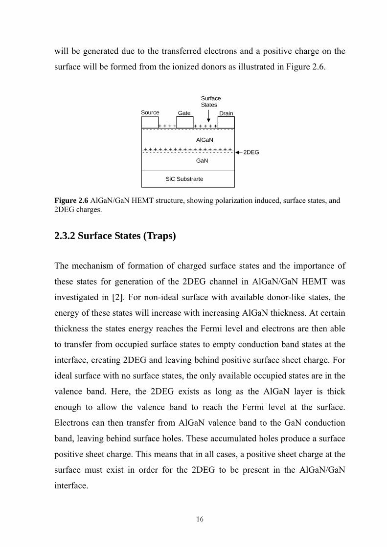
will be generated due to the transferred electrons and a positive charge on the
surface will be formed from the ionized donors as illustrated in Figure 2.6.
Surface
Figure 2.6 AlGaN/GaN H2DEG charges.
2.3.2 Surface State
The mechanism of for
these states for genera
investigated in [2]. Fo
energy of these states w
thickness the states en
to transfer from occup
interface, creating 2DE
ideal surface with no s
valence band. Here, t
enough to allow the
Electrons can then tra
band, leaving behind s
positive sheet charge. T
surface must exist in
interface.
- - - - - - - - - - - - - - - - - - - - - - - - - -
+ + + + + + + + + + + + + + + + + +AlGaN
GaN- - - - - - - - - - - - - - - - - - - - - - - - - -
+ + + + +
2DEG
SiC Substrarte
+ + + +
StatesGate DrainSource
EMT structure, showing polarization induced, surface states, and
s (Traps)
mation of charged surface states and the importance of
tion of the 2DEG channel in AlGaN/GaN HEMT was
r non-ideal surface with available donor-like states, the
ill increase with increasing AlGaN thickness. At certain
ergy reaches the Fermi level and electrons are then able
ied surface states to empty conduction band states at the
G and leaving behind positive surface sheet charge. For
urface states, the only available occupied states are in the
he 2DEG exists as long as the AlGaN layer is thick
valence band to reach the Fermi level at the surface.
nsfer from AlGaN valence band to the GaN conduction
urface holes. These accumulated holes produce a surface
his means that in all cases, a positive sheet charge at the
order for the 2DEG to be present in the AlGaN/GaN
16

The surface states act as electron traps located in the access regions between
the metal contacts. Proper surface passivation prevents the surface states from
being neutralized by trapped electrons and therefore maintains the positive
surface charge. If the passivation process is imperfect, then electrons, leaking
from the gate metal under the influence of a large electric field present during
high power operation, can get trapped [9]. The reduction in the surface charge
due to the trapped electrons will produce a corresponding reduction in the
2DEG charge, and therefore reduce the channel current. The amount of trapped
electrons and therefore the current reduction depends on the applied bias
voltages and the extent to which the device is overdriven beyond the linear
gain. The trapped electrons are modulated with the low frequency stimulating
voltages, and therefore can contribute to the 2DEG channel current. However,
they cannot follow the high frequency stimulating voltages, and therefore
produce a channel current reduction. This reduction in the current under RF
operation is called current dispersion, or more precisely, surface traps induced
current dispersion.
2.4 AlGaN/GaN HEMT Technology
2.4.1 Device Fabrication
The general structure of the investigated devices is shown in Figure 2.7. The
AlGaN/GaN HEMT structure was grown on SiC 2”-wafers using MOCVD
technology [10]. This substrate provides an excellent thermal conductivity of
3.5 W/cm, which is an order of magnitude higher than that of sapphire. The
epitaxial growth structure starts with the deposition of a 500 nm thick graded
AlGaN layer on the substrate to reduce the number of threading dislocations in
the GaN buffer layer due to the lattice mismatch between GaN and SiC layers.
These threading dislocations enhance the buffer traps [11], as will be explained
17

in the next section. A 2.7 µm thick highly insulating GaN buffer layer is then
deposited to get lower background carrier concentration and therefore increase
the electron mobility in the above unintentionally doped layers. The buffer
layer is followed by a 3 nm Al0.25Ga0.75N spacer, 12 nm Si-doped Al0.25Ga0.75N
supply layer (5x1018 cm-3), and 10 nm Al0.25Ga0.75N barrier layer. The spacer
layer is included to reduce the ionized-impurity scattering that deteriorates
electron mobility in the 2DEG. The spontaneous and piezoelectric polarization
of these Al0.25Ga0.75N layers on top of the buffer form a 2DEG at the
AlGaN/GaN interface, as explained in section 2.3. The whole structure is
capped with a 5 nm thick GaN layer to increase the effective Schottky barrier,
which improves the breakdown characteristics and decreases the gate leakage.
The measured 2DEG electron density and mobility, at room temperature, are
7.8×1012 cm-2 and 1400 cm2/Vs [10]. Device fabrication is accomplished using
0.5 µm stepper lithography, which results in an excellent homogeneity of the
electrical properties over the wafer [12].
Source Gate Drain
Figure 2.7
Source and drain
Ti/Al/Ti/Au/WSiN
morphology. Due to
Ti/Al/Ti/Au layers,
GaN-Cap 5 nm
AlGaN-Barrier 10 nm
AlGaN:Si-Supply 12 nm5x10 cm
AlGaN-Spacer 3 nm
GaN-Buffer 2700 nm
AlGaN GaN 300 nm→AlGaN 200 nm
SiC-Substrate
18 -3
- - - - - - - - - - - - - - - - - - - - - - - - - - - 2DEG
Epitaxial layer structure of the AlGaN/GaN HEMT [13].
ohmic contacts have a metallization consisting of
(10/50/25/30/120 nm) with improved edge and surface
the properties of the WSiN sputter deposition process, the
which are deposited by e-beam evaporation, are totally
18

embedded. The source and drain contacts are then rapidly thermal-annealed at
850 oC. After annealing, it was observed that the surface and contours of the
employed metallization with WSiN are still smooth and well-defined [10]. The
contact resistance is analyzed by TLM (Thermal Lens Microscope)
measurements with respect to thickness and composition of the different
metallization layers at different temperatures. The contact resistance is
determined to be 0.25-0.5 Ωmm under these conditions [10]. It is found that the
ohmic contact covered by WSiN is stable in electrical performance and
morphology for temperatures of 400 °C up to 120 hours.
Gate contacts are made from a Pt/Au metallization, and a gate length (LG) of
0.5µm is obtained using stepper lithography. Additionally, devices with LG less
than 0.3µm are written using a shaped electron beam tool (ZBA23-40kV) [14].
SiN passivation layer is then deposited to reduce the surface trapping induced
drain current dispersion. Field plate connected to gate at the gate pad and
deposited over the passivation layer was employed for some investigated
devices to improve the breakdown characteristics of the device. An air-bridge
technology using an electroplated Au is used to connect the source pads of
multifinger devices.
2.4.2 Fabrication Related Problems
2.4.2.1 Buffer Traps
Buffer traps refer to the deep levels located in the buffer layer or in the
interface between the buffer layer and the substrate. Under high electric field
condition, due to high drain-source voltage, electrons moving in the 2DEG
channel could get injected into the buffer traps. Due to the longer trapping time
constant (in the order of 0.1 ms [15]), the trapped electrons cannot follow the
high frequency signal and hence, they are not available for conduction. The
19

trapped electrons produce a negative charge, which depletes the 2DEG, and
therefore reduce the channel current. This reduction in the current under RF
operation is called current dispersion, or more precisely, buffer traps induced
current dispersion.
These traps are primarily related to the existing large number of threading
dislocation in the GaN layer due to the large lattice mismatch between the GaN
and the substrate. These threading dislocations manifest themselves as
electrons traps [11]. Therefore, to reduce these generated traps, a relaxation
layer is added between GaN buffer and the substrate, as provided in the last
section. Another source of traps is the buffer compensation process to obtain
high insulating material. Availability of background electron concentration in
the buffer material due to native shallow donors cannot be avoided. These
donors are mostly compensated by adding deep acceptors. If the buffer is not
completely compensated, then a leakage current through the buffer will be
generated. This leakage current deteriorates the pinch-off characteristic of the
device as shown in Figure 2.8a.
0 10 20 30-100
0
100
200
300
400
500
600
700
800
VDS (V)
I DS (m
A)
VGS from -6 V to 1 V in step of 1 V
Badpinch-off
0 10 20 30-100
0
100
200
300
400
500
600
700
800
900
VDS (V)
I DS (m
A)
VGS from -6 V to 1 V in step of 1 V
Kinkeffect
(a) (b)
Figure 2.8 (a) Bad pinch-off DC characteristics, measured in-house, of a 8x125 µm gate width AlGaN/GaN HEMT (wafer no. 713-2) related to the buffer leakage current, (b) kink effect in DC characteristics, measured in FBH, of a 8x125 µm gate width AlGaN/GaN HEMT (wafer no. 713-2) related to the buffer traps.
20

In the case of over-compensation, empty deep acceptors will be generated in
the buffer material. These empty acceptors behave as electron traps.
Optimization of the compensation process can reduce these traps [16]. The kink
effect in the DC characteristic, shown in Figure 2.8b, can be assumed as a
signature of buffer trapping effect. This effect is attributed to hot electrons
injected into the buffer traps under the influence of high drain voltage [16],
[17]. These trapped electrons deplete the 2DEG and result in a reduction of the
drain current for subsequent VDS traces.
2.5 AlGaN/GaN HEMT Performance
2.5.1 IV Characteristics
DC IV characteristics for 8x125 µm gate width AlGaN/GaN HEMT, measured
by IAF, are shown in Figure 2.9. As shown in the figure, the maximum zero
gate voltage current (IDSO) is equal to 745 mA. The drain knee voltage
(VDS,Knee) is approximately 5V, the pinch-off voltage (VPinch-off) is
approximately – 4V, and the extracted maximum extrinsic transconductance
(GM,max) is equal to 260 mS/mm. The breakdown voltage for this device is
approximately 60V [14]. The current collapse in the high current range is
attributed to self-heating of the device, due to high power dissipation, which
degrades the electrons saturation velocity and therefore reduces the current.
The self-heating effect, in our investigated devices, can generate an internal
temperature rise up to 120 °C [18]. This effect has significant impact on the
device performance under low frequency operation where stimulating signal is
slow enough to heat up the device. However, under high frequency operation
the internal temperature does not clearly change with the signal. This reduction
in the drain current under low frequency operation is called self-heating
21

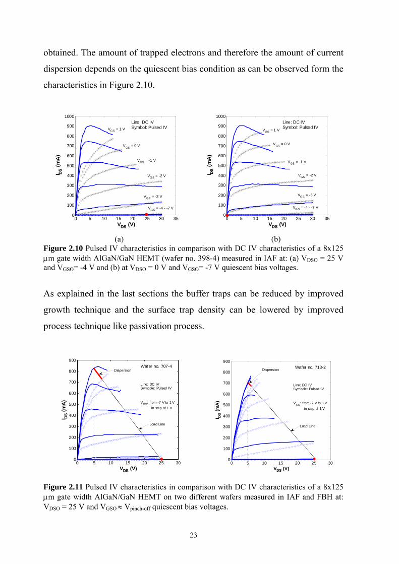
induced current dispersion. Pulsed IV characteristics for the same device in
comparison with the DC characteristics at different quiescent bias conditions
are shown in Figure 2.10. Since the quiescent bias voltages are in the pinch-off
region, the dissipated power and therefore self-heating effect, due to these
voltages, is very small. The pulse width of the applied gate and drain pulses is
equal to 1 µs with a period of 1 ms to reduce the self-heating of the device.
Therefore, the observed difference of the IV curve between DC and under
pulsed condition (current dispersion) is related mainly to the surface and buffer
trapping effects. As can be seen, current is reduced and knee voltage is
increased with pulsed operation. Therefore, the predicted output power based
on these characteristics will be lower than one expected from the DC
characteristics.
1000
F39
W
in
W
re
g
re
0 5 10 15 20 25 30 350
100
200
300
400
500
600
700
800
900
1000
VDS (V)
I DS (m
A)
VGS = 1 V
VGS = 0 V
VGS = -1 V
VGS = -2 V
VGS = -3 V
VGS = -4 - -7 V
-6 -4 -2 0 20
100
200
300
400
500
600
700
800
900
VGS (V)
I DS (m
A)
VDS = 0.25 V
VDS = 0.5 V
VDS = 1 V
VDS = 1.5 V
VDS = 2 V
VDS = 5 V
VDS = 10 V
VDS = 0 V
igure 2.9 DC IV characteristics of a 8x125 mm gate width AlGaN/GaN HEMT (wafer no. 8-4) measured in IAF.
ith pulse operation, the device is first pinched off, and electrons are injected
to traps (surface or buffer traps) under this high electric field condition.
hen the channel is turned on by a short pulse, the trapped electrons cannot
sponse in time. However, under DC condition, the gate bias is stepped
radually up from pinch off, giving enough time for the trapped electrons to
spond and emit from the traps. Thus the maximum channel current can be
22
obtained. The amount of trapped electrons and therefore the amount of current
dispersion depends on the quiescent bias condition as can be observed form the
characteristics in Figure 2.10.
0 5 10 15 20 25 30 350
100
200
300
400
500
600
700
800
900
1000
VDS (V)
I DS (m
A)
VGS = 1 V
VGS = 0 V
VGS = -1 V
VGS = -2 V
VGS = -3 V
VGS = -4 - -7 V
Line: DC IVSymbol: Pulsed IV
0 5 10 15 20 25 30 350
100
200
300
400
500
600
700
800
900
1000
VDS (V)
I DS (m
A)
Line: DC IVSymbol: Pulsed IV
VGS = -4 - -7 V
VGS = -3 V
VGS = -2 V
VGS = -1 V
VGS = 0 V
VGS = 1 V
(a) (b) Figure 2.10 Pulsed IV characteristics in comparison with DC IV characteristics of a 8x125 µm gate width AlGaN/GaN HEMT (wafer no. 398-4) measured in IAF at: (a) VDSO = 25 V and VGSO= -4 V and (b) at VDSO = 0 V and VGSO= -7 V quiescent bias voltages.
As explained in the last sections the buffer traps can be reduced by improved
growth technique and the surface trap density can be lowered by improved
process technique like passivation process.
0 5 10 15 20 25 300
100
200
300
400
500
600
700
800
900
VDS (V)
I DS (m
A)
Load Line
VGS: from -7 V to 1 V in step of 1 V
Line: DC IVSymbole: Pulsed IV
Wafer no. 707-4Dispersion
0 5 10 15 20 25 300
100
200
300
400
500
600
700
800
900
VDS (V)
I DS (m
A)
Dispersion Wafer no. 713-2
Line: DC IVSymbole: Pulsed IV
VGS: from -7 V to 1 V in step of 1 V
Load Line
Figure 2.11 Pulsed IV characteristics in comparison with DC IV characteristics of a 8x125 µm gate width AlGaN/GaN HEMT on two different wafers measured in IAF and FBH at: VDSO = 25 V and VGSO ≈ Vpinch-off quiescent bias voltages.
23

Figure 2.11 shows pulsed IV characteristics for a 8x125 µm gate width device
under same quiescent bias condition on wafer no. 707-4 of the first process and
wafer no. 713-2 of the second improved process. It can be seen from the
amount of dispersion the effect of device technology optimization in reducing
of the current dispersion.
2.5.2 RF Characteristics
The unity current gain frequency (ft) and the maximum oscillation frequency
(fmax) are useful figures of merit that can indicate the maximum achievable
performance of the device. ft is the frequency at which the short circuit current
gain, h21, is 1. ft can be extracted from S-parameter measurements since S-
parameters are converted into H-parameters and then h21 is plotted (in dB)
versus frequency using the equation
⎟⎟⎠
⎞⎜⎜⎝
⎛++−
−=
21122211
2121 )1)(1(
2log20)(SSSS
SdBh .
From the extrapolation of the h21 curve with the frequency axis, we can obtain
ft. Normally, ft is a good indication of the maximum achievable gain-bandwidth
for resistively terminated device. fmax is the frequency at which maximum
unilateral gain (MUG) is 1. It is obtained under the condition of conjugately
matched input and output of the device and canceling of the feedback gate-
drain impedance. This frequency is the maximum possible frequency to
achieve power amplification using the device. fmax can be extracted from the S-
parameter measurements using the following expression
⎥⎥⎦
⎤
⎢⎢⎣
⎡
−−= )
S11(S)
S11(log10)dB(MUG 2
22
2212
11
.
fmax then can be extrapolated from the curve of MUG versus frequency. The
values of ft and fmax, at certain bias condition, depend on the structure of the
24

device, which determine the values of the intrinsic parameters and the parasitic
elements. Figure 2.12 shows the extracted value of ft and fmax at different bias
points for a 8x125 µm gate width AlGaN/GaN HEMT. As shown in the figure,
the maximum value of ft for class AB operated device is approximately 27
GHz, while the maximum value of fmax is approximately 50 GHz.
-3.5 -3 -2.5 -2 -1.5 -1 -0.5 0 0.5 1
5
10
15
20
25
30
VGS (V)
ft (
GH
z)
VDS = 1 V
VDS = 2 V
VDS = 3 V
VDS = 5 V
VDS = 9 V
VDS = 11 V
VDS = 15 V
VDS = 17 V
VDS = 21 V
VDS = 27 V
VDS = 29 V
-3.5 -3 -2.5 -2 -1.5 -1 -0.5 0 0.5 1 0
10
20
30
40
50
60
VGS (V)
fm
ax (G
Hz)
VDS = 1 V
VDS = 2 V
VDS = 3 V
VDS = 5 V
VDS = 9 V
VDS = 11 V
VDS = 15 V
VDS = 17 V
VDS = 21 V
VDS = 27 V
VDS = 29 V
Figure 2.12 Measured unity gain frequency (ft) and maximum oscillation frequency (fmax) versus gate voltage for a 8x125 µm gate width AlGaN/GaN HEMT (wafer no. 713-2) at different drain voltages.
At lower voltages (lower drain current), fT increases with an increase of
voltages due to an increase of the transconductance. The decrease of fT value at
high voltages (high drain current) is related to the self-heating effect, which
reduces the value of electron velocity and therefore the transconductance.
15
FoΩ
37
11 13 15 17 19 21 23 259 27 11 13 15 17 19 21 23 259 27
9
11
13
7
Pin (dBm)
Gai
n (d
B)
Wafer No. 707-4Wafer No. 713-225
27
29
31
33
35
23
Pin (dBm)
Pou
t (d
Bm
)
Wafer No. 707-4Wafer No. 713-2
igure 2.13 Single-tone power sweep in-house measurements for class AB (IDS=0.2IDSS) perated 8x125 µm gate width AlGaN/GaN HEMT on two different wafers at 2 GHz in a 50 source and load environment.
25

fmax has the same trend as fT because they are correlated. It can also be observed
that the value of fmax increases with drain voltage. This increase is mainly
related to the decrease of gate-drain intrinsic capacitance with increasing the
drain voltage [19]. Power sweep measurements for the same two characterized
devices in Figure 2.11 (no. 707-4 and no. 713-2) are presented in Figure 2.13.
The measured output power here is less than that predicted from the DC IV
characteristics. This is related to the current dispersion as explained in the last
section. At low input power levels, the output power reduction is mainly related
to the trapping induced current dispersion because the self-heating due to the
biasing current (0.2 IDSS) is low. Therefore, the lower output power for the
device no. 707-4 is related mainly to the higher amount of trapping induced
current dispersion for this device. At high input power levels, self-heating due
to self-biasing of the distorted output signal will increase the output power
reduction. The effect of the current dispersion can also be observed from the
higher gain compression for devices when the highest power level was
achieved. Therefore, the trapping and self-heating effects play a very important
rule for limiting RF power characteristics of the device. These effects should be
considered for accurate modeling of the AlGaN/GaN HEMT for high power
amplifier design, which is the main goal of this research work.
References
[1] O. Ambacher, J. Smart, J. R. Shealy, N. G. Weimann, K. Chu, M. Murphy, W. J. Schaff, L. F. Eastman, R. Dimitrov, L. Wittmer, M. Stutzman, W. Rieger, and J. Hilsenbeck, “Two-dimensional electron gases induced by spontaneous and piezoelectric polarization in undoped and doped AlGaN/GaN heterostructures,” J. Appl. Phys., vol. 85, pp. 3222-3232, March 1999.
[2] J. P. Ibbetson, P. T. Fini, K. D. Ness, S. P. DenBars, J. S. Speck, and U. K. Mishra, “Polarization effects, surface states and the source of electrons in AlGaN/GaN heterostructure field effect transistors,” Appl. Phys. Letters, vol. 77, pp. 250-252, July 2000.
26
[3] G. J. Sullivan, J. A. Higgins, M. Y. Chen, J. W. Yang, Q. Chen, R. L. Pierson, and B. T. McDermott, “High power RF operation of AlGaN/GaN HEMTs grown on insulating silicon carbide substrates,” Electronics Letters, vol. 34, pp. 922-924, April 1998.
[4] S. T. Sheppard, K. Doverspike, W. L. Pribble, S. T. Allen, J. W. Palmour, L. T. Kehias, and T. J. Jenkins, “High-power microwave GaN/AlGaN HEMTs on semiinsulating silicon carbide substrates,” IEEE Electron Device Letters, vol. 20, pp. 161-163, April 1999.
[5] U. K. Mishra, P. Parikh, and Y. Wu, “AlGaN/GaN HEMTs–An overview of device operation and applications,” Proceeding of IEEE, vol. 90, pp. 1022-1031, June 2002.
[6] E. O. Johnson, “Physical limitations on frequency and power parameters of transistors,” IRE International Convention Record, vol. 13, pp. 27-34, March 1965.
[7] B. J. Baliga, “Semiconductor for high-voltage, vertical channel FET’s,” J. Appl. Phys., vol. 53, pp. 1759-1764, 1982.
[8] B. Ozpineci, and L. M. Tolbert,“ Comparison of wide-bandgap semiconductor for power electronics applications,” Technical Report, Oak Ridge National Laboratory, Oak Ridge, TN, December 2003.
[9] R. Vetury, N. Q. Zhang, S. Keller, and U. K. Mishra, “The impact of surface states on the DC and RF characteristics of AlGaN/GaN HFETs,” IEEE Trans. on Electron Devices, vol. 48, pp. 560-566, March 2001.
[10] R. Lossy, N. Chaturvedi, P. Heymann, J. Würfl, S. Müller, and K. Köhler, “Large area AlGaN/GaN HEMTs grown on insulating silicon carbide substrates,” Physica Status Solidi (a), vol. 194, pp. 460–463, December 2002.
[11] P. J. Hansen, Y. E. Strausser, A. N. Erickson, E. J. Tarsa, P. Kozodoy, E. G. Brazel, J. P. Ibbetson, U. Mishra, V. Narayanamurti, S. P. DenBaars, and J. S. Speck, “Scanning capacitance microscopy imaging of threading dislocations in GaN films grown on (0001) sapphire by metalorganic chemical vapor deposition,” Appl. Phys. Letters, vol. 72, pp. 2247–2249, May 1998.
[12] R. Lossy, J. Hilsenbeck, J. Würfl, and H. Obloh, “Uniformity and scalability of AlGaN/GaN HEMTs using stepper lithography,” Physica Status Solidi (a), vol. 188, pp. 263–266, November 2001.
[13] J. Würfl, “GaN-Hochfrequenzelektronik,” Workshop GaN-Elektronik, Bonn, April 2002.
[14] R. Lossy, P. Heymann, J. Würfl, N. Chaturvedi, S. Müller, and K. Köhler, “Power RF-operation of AlGaN/GaN HEMTs grown on insulating silicon carbide substrates,” European Gallium Arsenide & related III-V Compounds Application Symposium, September 2002, Milan, ISBN 0-86213-213-4.
[15] G. Meneghesso, G. Verzellesi, R. Pierobon, F. Rampazzo, A. Chini, U. K. Mishra, C. Canali, and E. Zanoni, “Surface-related drain current dispersion effects in AlGaN-
27

GaN HEMTs,” IEEE Trans. Microw. Theory Tech., vol. 51, pp. 1554-1561, October 2004.
[16] S. C. Binari, K. Ikossi, J. A. Roussos, W. Kruppa, Doewon Park, H. B. Dietrich, D. D. Koleske, A. E. Wickenden, and R. L. Henry, “ Trapping effect and microwave power performance in AlGaN/GaN HEMTs,” IEEE Trans. on Electron Devices, vol. 48, pp. 465-471, March 2001.
[17] S. Nuttinck, S. Pinel, E. Gebara, J. Laskar, and M. Harris,“ Cryogenic investigation of current collapse in AlGaN/GaN HFETS,” 11th GAAS Symposium, Munich, October 2003, pp. 213-215.
[18] R. Lossy, N. Chaturvedi, P. Heymann, K. Köhler, S. Müller, and J. Würfl,“ AlGaN/GaN HEMTs on silicon substrates for microwave power operation,” GaAs International Conference on Compound Semiconductor Manufacturing Technology, USA, pp. 327-330, 2003.
[19] Y. Okamoto, Y. Ando, T. Nakayama, K. Hataya, H. Miyamoto, T. Inoue, M. Senda, K. Hirata, M. Kosaki, N. Shibata, and M. Kuzuhara, “High-power recessed-gate AlGaN-GaN HFET with a field-modulating plate,” IEEE Trans. on Electron Devices, vol. 51, pp. 2217-2222, December 2004.
28

Chapter 3
Fundamentals of Active Device Modeling
In this chapter, fundamental principles of active device modeling will be
presented. First part will describe the general modeling approaches. Second
part will present the bottom-up modeling approach, which has been followed in
this research, and techniques of modeling the dynamic behavior of the device.
Finally, measurement techniques, which play an important role for defining the
accuracy of the device model, will be described.
3.1 Device Modeling Approaches
Device modeling methods can be classified into two main approaches. The first
one is physical modeling approach, which relies on physics-based parameters
that describe the geometry and technology of device. The second one is
empirical modeling approach, which depends on measured characteristics that
describe the behavior of the device.
3.1.1 Physical Modeling
In this modeling approach device performance can be predicted from physical
data describing the device. This data include carrier transport properties,
material characteristics, and the device geometry [1]-[7]. The main advantage
of this approach is that it describes the device operation in terms of the device
29

physics. Therefore, it is more applicable for device designer or circuit designer
who has some control over the device fabrication process. In this approach, the
device response is obtained by solving a set of coupled nonlinear differential
equations describing the internal field of the device and electrical charge
transport. These equations are complex and normally require numerical
methods to obtain solutions. In terms of simulation efficiency, this requires
longer time and larger memory storage, which is not practical for circuit design
purposes. Another problem with this modeling approach is the difficulty of
obtaining some of technology-based information. Also assumptions and
approximations, required to perform the device analysis, reduce the model
accuracy.
3.1.2 Empirical Modeling
Empirical modeling is also called measurement-based modeling because it
depends on measured data. Sometimes this modeling technique is also called
behavioral modeling because it depends on observed response due to
stimulation signal. Empirical models can be constructed using analytical
equations for the describtion of measured data. They are also termed
"analytical models" [8]-[13]. These models can also be constructed based upon
a lookup table developed from the measured data, and are called "table-based
models" [14]-[20]. Recently, a new empirical modeling approach has been
developed, which utilizes artificial neural network, or AAN [21]-[28].
Although the analytical models rely on mathematical representation of
observed input-output characteristics, the models, which are used for circuit
analysis, are always based on equivalent circuits. Therefore, these models can
also be classified as equivalent circuit models. The main advantages of the
analytical models are: computational efficiency, automatic data smoothing,
simplicity, and ability to simulate out of measurements range. The main
30
disadvantages are: limited accuracy due to use of simplified expression,
technology dependent, difficulty in extraction of the model fitting parameters,
and no physical meaning for the fitting parameters. The ANN models are
black-box models in that there is no assumption of particular analytical
functions or device physics related equivalent circuit. These models "learn" the
relationship between input and output from the measured data, and the models
can then efficiently calculate output for any applied input. The main advantage
of these models is that they can simulate accurately in spite of strong nonlinear
behavior of the device. But in the other side it has some disadvantages like the
validity range, which is limited to the conditions at which the measured data
are taken. Also these models do not give any information about the physics of
the device. The table-based models can also be considered as an equivalent
circuit based models, but instead of using mathematical expressions,
multidimensional spline functions are used to fit the measured data and only
fitting coefficients need to be stored. These models have some properties of
ANN models because they can also "learn" the behavior of the device.
Therefore, they are more accurate than the analytical models and ideal for
application where the functional form of the behavior is unknown. The physical
reliability of the models can be improved by using an equivalent circuit that
can fit the device physics. Data smoothing can be improved in these models by
using spline function that can maintain the continuity of the measured data.
One can conclude from this comparison that the table-based models can
compromise between simulation accuracy and implementation reliability.
Therefore, this approach will be followed in this research for large-signal
modeling of AlGaN/GaN HEMT.
31

3.2 Bottom-Up Modeling Technique
In bottom-up modeling technique a small-signal measurement is carried out
over a range of bias points, and large signal model is then determined from
small-signal models derived at those bias points. In the small-signal models the
intrinsic circuit is the main part, because it describes the nonlinear
characteristics of device. This intrinsic part is extracted by deembedding the
parasitic elements (extrinsic part) of the device. If the extrinsic part is not
completely deembedded, this will produce a residual parasitic effect, which
deteriorates the intrinsic circuit modeling and therefore the corresponding
derived large-signal model. To reduce the residual parasitic effect the small-
signal model topology should highly match the structure of the device. Also to
improve the voltage and frequency range capability the intrinsic circuit should
account for other effects, which are stimulated by high frequency and high
voltage conditions. More detail about physically relevant small-signal model
topology and the model parameter extraction process will be given in Chapter
4.
3.2.1 Quasi-Static FET Large-Signal Modeling
Quasi-static large-signal modeling approach is based on assumption that device
intrinsic elements are only voltage dependent [29]. Therefore, dynamic
response of the device can be predicted from static behavior of the device at
different bias condition. The principle benefit derived from this assumption is
the ability to define functional relationships under low frequency (quasi-static)
operation conditions, instead of using large-signal device characteristics at high
frequency, which are more time-consuming [30].
Under small-signal operation condition with signal time period larger than
trapping, self-heating, and carrier propagation time constants, the intrinsic part
32

of the device can be modeled with a simplified equivalent circuit shown in
Figure 3.1 [31].
Ggdf
Fi
The equiv
⎢⎣
⎡=
GY
The real p
large-sign
values of
characteri
the voltag
gsg VI
(
gsg VQ (
Gm gsVVgs Vds
g d
s s
Ggsf Cgs
Cgd
Gds Cds
gure 3.1 Intrinsic quasi-static small-signal equivalent circuit model [31].
alent circuit Y-parameter matrix is given by
⎥⎦
⎤+++−−
−−+++)(
)(
gddsgdfdsgdgdfm
gdgdfgdgsgdfgsf
CCjGGCjGGCjGCCjG
ωωωω
. (3.1)
art of the Y-parameter corresponds to incremental values of a current
al function, while the imaginary part corresponds to incremental
a charge large-signal function [31]. Therefore, the large-signal
stics of the device can be obtained by path independent integrals of
e-dependent Y-parameters as follow [31]:
[ ]
∫
∫
−
++=
ds
ds
gs
gs
V
Vgsgdf
V
Vdsgdfdsgsfdsgsgds
dVVVG
dVVVGVVGVVIV
0
0
),(
),(),(),(), 0000
(3.2)
[ ] ∫∫ −+=ds
ds
gs
gs
V
Vgsgd
V
Vdsgddsgsds dVVVCdVVVCVVCV
00
),( ),(),(), 00 (3.3)
33

∫
∫
++
−+=
ds
ds
gs
gs
V
Vgsgdfgsds
V
Vdsgdfdsmdsgsddsgsd
dVVVGVVG
dVVVGVVGVVIVVI
0
0
)],(),([
)],(),([),(),( 0000
(3.4)
[ ]∫ ∫ ++−=gs
gs
ds
ds
V
V
V
Vgsgdgsdsdsgddsgsd dVVVCVVCdVVVCVVQ
0 0
),(),( ),(),( 0 (3.5)
The integration constant of Qg and Qd can be assumed equal to zero because the
current contribution is calculated from the time derivative of these quantities.
Thus the quasi-static large-signal model of the device consists at least of two
sources (current and charge) at the gate and the drain as shown in Figure 3.2.
The current sources account for conduction currents, while the charge sources
account for displacement currents [16].
g d
3.2.2 No
Quasi-stat
active dev
condition.
current di
Therefore
source sh
the device
Vgs Vds
s s
+ +Q V Vg gs ds( , )I V Vg gs ds( , ) Q V Vd gs ds( , ) I V Vd gs ds( , )
Figure 3.2 Quasi-static large-signal model.
n-Quasi-Static FET Large-Signal Modeling
ic assumption is a good first-order approximation in modeling of
ice, but does not hold in the whole range of different operation
As explained in the last chapter, trapping and self-heating induced
spersions have strong impact on the RF performance of the device.
, non-quasi-static implementation for the large-signal drain current
ould be used to predict this effect. Also at high frequency operation,
channel charge under the gate does not response immediately to the
34
stimulation signal [32], [33]. This requires a relaxation time to build up. This
effect results in quadratic frequency dependency of measured Y11 at high
frequency [34]. Therefore, the large- and small signal model should be
modified to simulate this effect. Also the device channel transconductance, Gm,
cannot response instantaneously to changes in the gate voltage at high
frequency. Therefore, time delay inherent to this process should be accounted
in the small-signal model.
Ggdf
The high
using a te
resistance
parameter
voltage is
Figure 3.
including
the topolo
small-sign
topology,
shown in
symmetri
while Qgs
Vgs Vds
g d
s s
Ggsf Cgs
Cgd
Gds Cds
Ri
Rgd
Gm gse V-jωτ
Figure 3.3 Intrinsic non-quasi-static linear device equivalent circuit.
frequency simulation of the small-signal model can be improved by
n elements model shown in Figure 3.3 [35]. In this model, the series
s Ri and Rgd, account for the quadratic frequency dependency of Y-
s. The transconductance time delay with respect to the applied gate
described by transit time, τ. In the large-signal model, shown in
2, the simplest way to approximate the charge relaxation is by
a series bias-dependent resistance by each charge source. However,
gy of the modified large-signal model will not be consistent with the
al model shown in Figure 3.3. Therefore, large-signal model
shown in Figure 3.4, has higher consistency than the model topology
Figure 3.2 [14], [31], [35]. This topology also can reflect the
cal structure of the device especially at low drain-source voltages,
≈ Qgd [12].
35
Vgs Vds
g d
s s
+
+
Q V Vgs gs ds( , )I V Vgs gs ds( , )
Q V Vgd gs ds( , )
I V Vgd gs ds( , )
R V Vi( , )gs ds
R V Vgd( , )gs ds
I V Vds gs ds( , )
Figure 3.4 Non-quasi-static large-signal model.
Assuming that Ggsf is only dependent on the gate-source voltage, the gate
current sources, Igs and Igd, can be obtained using (3.2) by splitting the total
gate current as follow:
dVVVGVVIVVIgs
gs
V
Vdsgsfdsgsgsdsgsgs ),(),(),(
0
000 ∫+= (3.6)
∫∫ −+=ds
ds
gs
gs
V
Vgsgdf
V
Vdsgdfdsgsgddsgsgd dVVVGdVVVGVVIVVI
00
),( ),(),(),( 000 . (3.7)
To incorporate the effect of Cgs, Cgd, and Cds while maintaining the consistency
of the large-signal model, the charge sources, Qgs and Qgd, can be formulated as
follow [36]:
∫∫ +=ds
ds
gs
gs
V
Vgsds
V
Vdsgsdsgsgs dVVVCdVVVCVVQ
00
),( ),(),( 0 (3.8)
∫∫ +−=ds
ds
gs
gs
V
Vgsgdgsds
V
Vdsogddsgsgd dVVVCVVCdVVVCVVQ
00
)],(),([ ),(),( . (3.9)
36
3.2.2.1 Traps Induced Dispersion Modeling
There are different methods for modeling the non-quasi-static effect in the
drain current due to the traps induced dispersion. One of these methods, which
followed by Root [14], [37], [38] based on single-pole function to describe the
transition between DC and RF current values as follow:
),(1
),(1
1),( dsgsRFdsdsgs
DCdsdsgsds VVI
jjVVI
jVVI
ωτωτ
ωτ ++
+= (3.10)
where IdsDC is the measured DC drain current, Ids
RF is the calculated RF current
using (3.4), ω is the operating frequency, and τ is the trapping time constant.
The main limitation of this approach is that it cannot efficiently simulate the
low frequency transition range between DC and RF. Therefore the model is not
suitable for memory effect analysis [39], [40].
Another method for modeling the trapping induced dispersion was developed
by Werthof and Kompa [31], [41]. The non-quasi-static current source was
formulated as follows:
),(),(),(),( dsgscorrdsgscorrdsgsDCdsdsgsds VVIVVIVVIVVI ++= (3.11)
where Icorr and corrI are defined by
∫
∫
−+
−=
ds
ds
gs
gs
V
Vgs
DCdsgs
RFds
V
Vds
DCmds
RFmdsgscorr
dVVVGVVG
dVVVGVVGVVI
0
0
)],(),([
)],(),([),( 00
(3.12)
∫
∫
−+
−=
ds
ds
gs
gs
V
Vgs
DCdsgs
RFds
V
Vds
DCmds
RFmdsgscorr
dVVVGVVG
dVVVGVVGVVI
0
0
)],(),([
)],(),([),( 00
(3.13)
DCdsI is the measured DC drain current and Icorr describes an additional current
contribution originating from RF transconductance and output conductance
37
dispersion. corrI accounts for the self-biasing effect at high input power
operation. This effect results in shifting of dynamic operating point, which
controls the amount of current dispersion. This approach is more suitable than
the first one especially for devices having strong trapping induced dispersion.
The main limitation of this approach is the difficulty of implantation in ADS®
(Advanced Design System) software [74].
In these two methods, the RF drain current is calculated by a path integral,
assuming that the intrinsic channel conductances, GmRF and Gds
RF, satisfy the
integral path-independency condition. This condition is valid for small devices
with insignificant self-heating and, therefore, GmRF and Gds
RF values are mainly
related to the bias voltages. However, this is not the case for large high power
devices [42]. Because inherent self-heating during the devices S-parameter
measurements deteriorates characterization accuracy of the trapping induced
current dispersion.
A third method for modeling the trapping induced current dispersion, which
will be followed in this dissertation, can give justified solution. This method is
based on the assumption that under operating frequency well above the
dispersion cut-off frequency, the trapping mechanism is mainly controlled by
the DC components of the applied voltages, Vgs(t) and Vds(t) [17]. Therefore
the drain current under negligible self-heating effect can be modeled as
)( ),(
)( ),(),(),( ,
dsodsdsgsD
gsogsdsgsGdsgsDC
isodsdsgsds
VVVV
VVVVVVIVVI
−+
−+=
α
α (3.14)
where Ids,isoDC is an isothermal DC current under constant ambient temperature
and negligible self-heating conditions. αG and αD model the deviation in the
drain current due to the surface trapping and buffer trapping, respectively.
Here, the drain current is considered as a summation of dispersionless DC
current and other dispersion contributions due to the RF current components.
The model fitting parameters, Ids,isoDC, αG and αD are extracted from pulsed IV
38

characteristics, which do not heat up the device, as will be explained in chapter
5. Therefore, the model parameters are obtained directly from RF
measurements instead of using the described indirect path integral method.
Also under negligible self-heating characterization the model can accurately
describe the trapping induced dispersion. To improve the modeling of the
transition between DC and RF, circuit level implementation shown in Figure
3.5 is used. The RC high pass configuration, in the gate and drain sides, can
simulate a smooth transition between DC and RF by feeding (Vgs-Vgso) and
(Vds-Vdso) RF voltages back to the drain current model.
Figure 3.5 Non-quasi-static large-signal model including trapping induced dispersion.
Vgs Vds
g d
s s
+
+
Q V Vgs gs ds( , )I V Vgs gs ds( , )
Q V Vgd gs ds( , )
I V Vgd gs ds( , )
R V Vi( , )gs ds
R V Vgd( , )gs ds
I V Vds gs ds( , ),V ,Vgso dso
CDT
RDT
CGT
RGT ( )V Vds dso - ( )V Vgs gso -
3.2.2.2 Self-Heating Induced Dispersion Modeling
In general, self-heating dependent drain current can be described as [43]:
)]()(1[ ),(),( thtPVVIVVI dissdsgsdsodsgsds ∗−= λ (3.15)
where Idso is an isothermal current at constant ambient temperature, λ is a
function of thermal resistance of the device structure and the temperature
dependence of the drain current. Pdiss(t) is the device instantaneous power
dissipation and h(t) is a thermal impulse response. In frequency domain this
equation can be written as:
39

)]( )(1[ ),(),( ωωλ HPVVIVVI dissdsgsdsodsgsds −= . (3.16)
The thermal frequency response function H(ω) can be defined as [43]:
)1()/1()/1(1)( n
cn
o jjH −++
=ωωωω
ω (3.17)
where ωc and ωo are the upper and lower roll off frequencies and n is the order.
As a first order approximation, the thermal frequency response can be
described with a single pole transfer function
)/1(1)(
ojH
ωωω
+= . (3.18)
Hence the model in (3.16) will simulate a current reduction due to self-heating
under low frequency operation condition and very little thermal response under
high operating frequencies. Generally, λ is nonlinear function describing the
nonlinear behavior of the device self-heating with increasing the power
dissipation [44]. However, under the assumption of constant thermal
conductivity of the device substrate, the current model can be written as [45]:
)]()(1[ ),(),( ωω HPRKVVIVVI dissthTdsgsdsodsgsds −= (3.19)
where KT is a thermal constant, which describes the dependency of the drain
current on the device self-heating. The self-heating, which is typically signed
as ∆T(ω), corresponds here to the multiplication of the device thermal
resistance Rth and Pdiss(ω). Thus, the self-heating process can be implemented
using a simple low pass circuit as shown in Figure 3.6. Similar modeling
approaches for the self-heating induced current dispersion have been used in
many large-signal models [46]-[52]. The thermal transient response of the
device is described by Cth, which depends on the device material and geometry.
This element can be obtained analytically based on the device physics [53] or
directly from temperature measurements [54]. The thermal resistance can also
be obtained analytically [45], [55], or from measurements [56].
40

Figure 3.6 Equivalen
In our procedure for m
approach and the drain
follows:
gDC
isodsdsgsds VIVVI (),( ,=
where Ids,isoDC is an iso
accounts for the device
drain current with the de
Therefore, with this for
data or special measurem
The same low pass circu
equivalent circuit in F
Therefore, the model can
power and “quasi-static
voltage. The extraction p
model implementation an
3.3 Device Chara
Device characterization
and accuracy of the d
parameter extraction dep
∆TRth CthP ( )ωdiss
t circuit implementation for device self-heating process.
odeling of AlGaN/GaN HEMT, we used a similar
current including only the self-heating was defined as
dissodsgsTdss PVVV ),(), α+ (3.20)
thermal DC current and αT is a fitting parameter
thermal resistance and the nonlinear variation of the
vice self-heating. Pdisso is the average dissipated power.
mulation, there is no need for technology dependent
ents to determine the value of the thermal resistance.
it in Figure 3.6 will be added to the large-signal model
igure 3.5 to include the self-heating simulation.
simulate the self-heating due to the average dissipated
” dissipated power produced by slowly time varying
rocedure of αT(Vgs,Vds) and the complete large-signal
d verification will be presented in chapter 5.
cterization
is one of the main reasons that defines the reliability
evice model. The reliability of small-signal model
ends strongly on the measurement uncertainty as will
41

be explained in chapter 4. Also for measurement-based large-signal model,
simulation accuracy depends mainly on the quality of the measurements.
Therefore, due to the importance of the measurements, this section will give an
overview about the main measurements, which are usually used for the device
characterization and modeling.
3.3.1 IV Measurements
3.3.1.1 DC IV Measurements
DC IV measurements of active devices are very fundamental measurements for
device modeling. The DC measurement set-up could be part of high frequency
on-wafer (S-parameter) measurement system or included in a pulsed IV
measurement system. Through the DC measurements, biasing and
measurements are accomplished simultaneously. The device ports can be
biased through RF coplanar probes. Due to the inherent self-heating through
these measurements, the delay time between each two measurements should be
high enough to cool down the device, and, therefore, uncorrelated
measurements can be obtained. Such measurements cannot be used for RF
device characterization because in RF situation the device temperature does not
clearly change with the applied RF signal. Safe operation limitations
(maximum voltage, maximum current, and maximum power) should be taken
into account through the device characterization. For modeling of the gate-
forward and gate-breakdown the device need to be characterized beyond these
rate values. The DC IV measurement system cannot be used for this purpose
because this can lead to physical (chemical) alteration for the device properties,
or local destruction in the device structure.
42

3.3.1.2 Pulsed IV Measurements
Pulsed IV measurements can overcome the main limitations of the
corresponding DC measurements. As mentioned in the last section, modeling
of self-heating induced current dispersion requires isothermal measurements.
Also, due to temperature dependency of the trapping mechanism [49], this
effect should be characterized under negligible self-heating. The pulsed IV
measurements can approach the isothermal condition, since all IV
characteristics can be obtained at a constant device temperature defined by
quiescent bias condition and ambient temperature. The pulsed IV
measurements under appropriate quiescent bias conditions can also be used for
trapping induced dispersion characterization [57]. These measurements also
offer a way to investigate the characteristic of the device in ranges where
damage or deterioration can occur, because it is possible to extend the range of
measurements under pulsed conditions, without harm [58].
3.3.2 S-Parameter Measurements
The most common measurements utilized for characterization of active devices
for small-sgnal model parameters extraction purposes are S-parameter
measurements. These measurements can characterize small-signal performance
of the device under certain bias condition. Under this condition, the
measurements are used to determine a unique set of values for small-signal
equivalent circuit elements. The process of extracting the small-signal
equivalent circuit elements will be explained in chapter 4. The measurements
can be automated to characterize a large range of bias points. From the
dependency of the equivalent circuit elements on bias condition, large-signal
model for the device can be derived, as explained in Section 3.2. For more
accuracy, the measurements need to be performed over appropriate bias range.
43

More measurements should be in strong nonlinear regions (ohmic, breakdown,
and forward) [59]. The device S-parameter measurements can be performed up
to 120 GHz [60]. Accuracy of device measurements, however, depends mainly
on the system calibration and the deembedding of the device test fixture [61]-
[63].
3.3.3 Low Frequency Dispersion Measurements
Low frequency dispersion measurements are used to characterize the drain
current dispersion in terms of channel transconductance and output
conductance. It is reported that the transconductance dispersion is mainly
related to surface traps [64], while output conductance is mainly related to the
buffer traps [65]. Therefore, these measurements can characterize the
frequency dependency of the surface and buffer traps induced dispersion
described in current model (3.14) and implemented in Figure 3.5. Appropriate
values for the R and C circuit elements at the gate and drain sides of this
model, can be extracted from the corner frequencies of the transconductance
and output conductance frequency response. The low frequency dispersion can
be measured using measurement set-up similar to one described in [66] or
using low frequency signal analyzer [67].
3.3.4 Large-Signal Measurements
3.3.4.1 Load-Pull Measurements
Load-Pull measurements are an experimental technique for direct
characterization of large-signal performance of active devices under certain
input and output termination impedances. In this technique, the output and
input impedances can be tuned to find an optimal condition that fulfills
particular performance parameter (i.e., maximum output power, maximum
44

power added efficiency, etc). These measurements can be classified into
passive load-pull and active load-pull measurements. In the first one, the
measurements are performed using passive load and output reflection
coefficients are achieved by changing the load mechanically [68]. The main
disadvantage of this method is that it is not possible to obtain the complete
range of the reflection coefficient due to the loss in transmission line and
different components used. The second technique, which is called active load-
pull, can overcome the reflection coefficient range limitation. In the active
load-pull system, the load variation is realized electronically by injecting an
incident wave at the output of the device [69]. This system was extended
toward multi-harmonic load-pull measurements [70]-[72], which allow
independent load tuning of the fundamental signal and its harmonics. The load-
pull measurements can be combined with waveform measurements to give
more insight into the nonlinear characteristics of the measured device [73]. In
addition to experimental investigation, these measurements can be used for
large-signal model verification as will be presented in Chapter 5.
References
[1] R. A. Pucel, D. J Masse, and C. F. Krumm, “Noise performance of gallium arsenide field-effect transistors,” IEEE J. Solid State Circuits, vol. 11, pp. 243-255, April 1976.
[2] T. Wada and J. Frey, “Physical basis of short-channel MESFET operation,” IEEE Trans. on Electron Devices, vol. 26, pp. 476-490, April 1979.
[3] J. M. Golio and R. J. Trew, “Profile studies of ion-implanted MESFET's,” IEEE Trans. on Electron Devices, vol. 30, pp. 1844-1849, December 1983.
[4] C. Moglestue, “Monte Carlo particle simulation of a quantum well heterojunction field-effect transistor: Comparison with experimental data,” J. Appl. Phys., vol. 80, pp. 1499-1503, August 1996.
[5] S. Wu, R. T. Webster, and A. F. M. Anwar, “Physics-based intrinsic model for AlGaN/GaN HEMTs,” MRS Internet Journal of Nitride Semiconductor Research, vol. 4S1, Art. G6.58, 1999.
45

[6] J. D. Albrecht, P. P. Ruden, S. C. Binari, and M. G. Ancona, “AlGaN/GaN heterostructure field-effect transistor model including thermal effects,” IEEE Trans. on Electron Devices, vol. 47, pp. 2031-2036, November 2000.
[7] Rashmi, A. Kranti, S. Haldar, M. Gupta, and R. S. Gupta, “Comprehensive analysis of small-signal parameters of fully strained and partially relaxed high Al-content lattice mismatched AlmGa1-mN/GaN HEMTs,” IEEE Trans. Microw. Theory Tech., vol. 51, pp. 607-617, February 2003.
[8] W. R. Curtice, “A MESFET model for use in the design of GaAs integrated circuits,” IEEE Trans. Microw. Theory Tech., vol. 28, pp. 448-456, May 1980.
[9] Y. Tajima, B. Wrona, and K. Mishima, “GaAs FET large-signal model and its application to circuit designs,” IEEE Trans. on Electron Devices, vol. 28, pp. 171-175, February 1981.
[10] A. Materka and T. Kacprzak, “Computer calculation of large-signal GaAs FET amplifier characteristics,” IEEE Trans. Microw. Theory Tech., vol. 33, pp. 129-135, February 1985.
[11] W. R. Curtice and M. Ettenberg, “A Nonlinear GaAs FET model for use in the design of output circuits for power amplifiers,” IEEE Trans. Microw. Theory Tech., vol. 33, pp. 1383-1394, December 1985.
[12] H. Statz, P. Newman, I. W. Smith, R. A. Pucel, and H. A. Haus, “GaAs FET device and circuit simulation in SPICE,” IEEE Trans. on Electron Devices, vol. 34, pp. 160-169, February 1987.
[13] I. Angelov, H. Zirath, and N. Rorsman, “A new empirical nonlinear model for HEMT and MESFET devices,” IEEE Trans. Microw. Theory Tech., vol. 40, pp. 2258-2266, December 1992.
[14] D. E. Root, S. Fan, and J. Meyer, “Technology-independent large-signal FET models: a measurement-based approach to active device modeling,” Proceedings of 15th ARMMS Conf., pp. 1-21, September 1991.
[15] A. Werthof and G. Kompa, “A unified consistent DC to RF large-signal FET model covering the strong dispersion effects of HEMT devices,” 22th European Microwave Conf. Proc., Helsinki, pp. 1091-1096, September 1992.
[16] R. R. Daniels, A. T. Yang, and J. P. Harrang, “A universal large/small signal 3-terminal FET model using a nonquasi-static charge-based approach,” IEEE Trans. on Electron Devices, vol. 40, pp. 1723-1729, October 1993.
[17] F. Filicori, G. Vannini, A. Santarelli, A. Mediavilla, A. Tazón, and Y. Newport, “Empirical modeling of low-frequency dispersive effects due to traps and thermal phenomena in III-V FET's,” IEEE Trans. Microw. Theory Tech., vol. 43, pp. 2972-2981, December 1995.
[18] M. F. Barciela, P. J. Tasker, M. Demmler, and E. Sanchez, “A simplified non quasi-static table-based FET model,” 26th European Microwave Conf. Proc., Prague, pp. 20-23, September 1996.
46

[19] D. Schreurs, “Table-based large-signal models based on large-signal measurements,” IEEE MTT-S Workshop: New Directions in Nonlinear RF and Microwave Characterization, San Francisco, paper 7, June 1996.
[20] I. Schmale, “Entwicklung eines konsistenten elektrothermischen Großsignalmodells für Feldeffekttransistoren als Grundlage für den zuverlässigen Entwurf monolithischer Frequenzverdoppler,” Doctoral Thesis (in German), Department of High Frequency Engineering, University of Kassel, Kassel, Germany, 1999.
[21] A. H. Zaabab, Q. J. Zhang, and M. S. Nakhla, “A neural network modeling approach to circuit optimization and statistical design,” IEEE Trans. Microw. Theory Tech., vol. 43, pp. 1349-1358, June 1995.
[22] K. Shirakawa, M. Shimiz, N. Okubo, and Y. Daido, “A large-signal characterization of an HEMT using a multilayered neural network,” IEEE Trans. Microw. Theory Tech., vol. 45, pp. 1630-1633, September 1997.
[23] A. H. Zaabab, Q. J. Zhang, and M. S. Nakhla, “Device and circuit-level modeling using neural networks with faster training based on network sparsity,” IEEE Trans. Microw. Theory Tech., vol. 45, pp. 1696-11704, October 1997.
[24] J. Rousset, Y. Harkouss, J. M. Collantes, and M. Campovecchio, “An accurate neural network model of FET for intermodulation and power analysis,” 26th European Microwave Conf. Proc., Prague, pp. 16-19, September 1996.
[25] J. A. Garcia, A. Tazon Puente, A. Mediavilla Sanchez, I. Santamaria, M. Lazaro, C. J. Pantaleon, and J. C. Pedro, “Modeling MESFETs and HEMTs intermodulation distortion behavior using a generalized radial basis function network,” International Journal of RF and Microwave Computer-Aided Engineering, vol. 9, pp. 261-276, May 1999.
[26] F. Giannini, G. Leuzzi, G. Orengo, and M. Alberini, “Small-signal and large-signal modeling of active devices using CAD-optimized neural networks,” International Journal of RF and Microwave Computer-Aided Engineering, vol. 12, pp. 71-78, January 2002.
[27] L. Zhang, J. Xu, M. Yagoub, R. Ding, and Q. Zhang, “Neuro-space mapping technique for nonlinear device modeling and large signal simulation,” IEEE MTT-S International Microwave Symposium Dig., Philadelphia, PA, pp. 173-176, June 2003.
[28] L. Zhang, J. Xu, M. Yagoub, R. Ding, and Q. Zhang, “Efficient analytical formulation and sensitivity analysis of neuro-space mapping for nonlinear microwave device modeling,” IEEE Trans. Microw. Theory Tech., vol. 53, pp. 2752-2767, September 2005.
[29] C. Rauscher and A. Willing, “Simulation of nonlinear microwave FET performance using a quasi-static model,” IEEE Trans. Microw. Theory Tech., vol. 27, pp. 834-840, October 1979.
[30] C. Rauscher, “Quasi-static modeling of microwave field-effect transistor for use in nonlinear circuit design,” International IEEE Workshop on Experimentally Based FET
47

Device Modelling and Related NonlinearCircuit Design, University of Kassel, Kassel, Germany, pp. 19.1-19.8, July 1997.
[31] G. Kompa, “Modelling of dispersive microwave FET devices using a quasi-static approach,” International Journal of RF and Microwave Computer-Aided Engineering, vol. 5, pp. 173-194, 1995.
[32] S.-Y. Oh, D. E. Ward, and R. W. Dutton, “Transient analysis of MOS transistors,” IEEE Trans. on Electron Devices, vol. 27, pp. 1571-1578, August 1980.
[33] M. Chan, K. Y. Hui, C. Hu; and P. K. Ko, “A robust and physical BSIM3 non-quasi-static transient and AC small-signal model for circuit simulation,” IEEE Trans. on Electron Devices, vol. 45, pp. 834-841, April 1998.
[34] M. Barciela, P. Tasker, Y. Roca, M. Demmler, H. Massler, E. Sanchez, M. Francos, and M. Schlechtweg, “A simplified broad-band large-signal nonquasi-static table-based FET model,” IEEE Trans. Microw. Theory Tech., vol. 48, pp. 395-405, March 2000.
[35] I. Schmale and G. Kompa, “A physics-based non-linear FET model including dispersion and high gate-forward currents,” International IEEE Workshop on Experimentally Based FET Device Modelling and Related Nonlinear Circuit Design, University of Kassel, Kassel, Germany, pp. 27.1-27.7, July 1997.
[36] I. Schmale and G. Kompa, “An improved physics-based nonquasi-static FET-model,” 27th European Microwave Conf. Proc., Jerusalem, pp. 328-330, September 1997.
[37] D. E. Root, “Foundations of measurement-based active device modeling for circuit simulation,” International IEEE Electromagnetics in Aerospace and Applications Conference, pp. 141-146, Turin, Italy, September 1993.
[38] D. E. Root, “Analysis and exact solutions of relaxation-time differential equation describing non quasi-static large signal FET models,” 24th European Microwave Conf. Proc., Cannes, France, pp. 854-859, Septembre 1994.
[39] J. Brinkhoff and A. E. Parker, “Charge trapping and intermodulation in HEMTs,” IEEE MTT-S International Microwave Symposium Dig., Forth Worth, TX, pp. 799-802, June 2004.
[40] A. E. Parker and J. G. Rathmell, “Bias and frequency dependence of FET characteristics,” IEEE Trans. Microw. Theory Tech., vol. 51, pp. 588-592, February 2003.
[41] A. Werthof, “Experimentelle Modellierung aktiver Bauelemente für die Simulation nichtlinearer Mikrowellenschaltungen,” Doctoral Thesis (in German), Department of High Frequency Engineering, University of Kassel, Kassel, Germany, 1994.
[42] C. J. Wei, Y. A. Tkachenko, and D. Bartle, “Table-based FET model assembled from small-signal models,” IEEE Trans. Microw. Theory Tech., vol. 47, pp. 700-705, June 1999.
[43] A. E. Parker and J. G. Rathmell, “Broad-band characterization of FET self-heating,” IEEE Trans. Microw. Theory Tech., vol. 53, pp. 2424-2429, July 2005.
48

[44] W. B. Joyce, “Thermal resistance of heat sinks with temperature-dependent conductivity,” Solid State Electronics, vol. 18, pp. 321-322, 1975.
[45] H. F. Cooke, “Precise technique finds FET thermal resistance,“ Microwaves & RF (ISSN 0745-2993), vol. 25, pp. 85-87, August 1981.
[46] A. J. Mccamant, G. D. Mccormack, and D. H. Smith, “An improved GaAs MESFET model for SPICE,” IEEE Trans. Microw. Theory Tech., vol. 38, pp. 822-824, June 1990.
[47] J. Meyer, D. E. Root, and K. Poulton, “Dynamic electro-thermal modeling,” International Microwave Symposium Workshop, Atlanta, Georgia, June, 1993.
[48] I. Angelov, N. Rorsman, J. Stenarson, M. Garcia, and H. Zirath, “An empirical table-based FET model,” IEEE Trans. Microw. Theory Tech., vol. 47, pp. 2350-2357, December 1999.
[49] P. C. Canfield, S. C. F. Lam, and D. J. Allstot, “Modeling of frequency and temperature effects in GaAs MESFETs,” IEEE J. Solid State Circuits, vol. 25, pp. 299-306, February 1990.
[50] A. E. Parker and D. J. Skellern, “A realistic large-signal MESFET model for SPICE,” IEEE Trans. Microw. Theory Tech., vol. 45, pp. 1563-1571, September 1997.
[51] C.-J. Wei, A. Y. Tkachenko, and D. Bartle, “An accurate large-signal model of GaAs MESFET which accounts for charge conservation, dispersion, and self-heating,” IEEE Trans. Microw. Theory Tech., vol. 46, pp. 1638-1644, November 1998.
[52] F. Filicori, A. Santarelli, G. Vannini, and V. A. Monaco, “A “backgating” model including self-heating for III-V FETs,” GAAS Symposium, Amsterdam, pp. 462-467, October 1998.
[53] V. Rizzoli, A. Lipparini, V. D. Esposti, F. Mastri, and C. Cecchetti, “Simultaneous thermal and electrical analysis of nonlinear microwave circuits,” IEEE Trans. Microw. Theory Tech., vol. 40, pp. 1446-1455, July 1992.
[54] R. Gaska, A. Osinsky, J. W. Yang, and M. S. Shur, “Self-heating in high-power AlGaN-GaN HFETs,” IEEE Electron Device Letters, vol. 19, pp. 89-91, March 1998.
[55] A. M. Darwish, A. J. Bayba, and A. H. Hung, “Accurate determination of thermal resistance of FETs,” IEEE Trans. Microw. Theory Tech., vol. 53, pp. 306-313, January 2005.
[56] J. Park, M. W. Shin, and C. C. Lee, “Thermal modeling and measurement of AlGaN-GaN HFETs built on sapphire and SiC substrates,” IEEE Trans. on Electron Devices, vol. 51, pp. 1753-1759, November 2004.
[57] C. Charbonniaud, S. De Meyer, R. Quere, and J. P. Teyssier, “Electrothermal and trapping effects characterization of AlGaN/GaN HEMTs,” 11th GAAS Symposium, Munich, pp. 201-204, October 2003.
49

[58] J. Scott, J. G. Rathmell, A. Parker, and Mohamed Sayed, “Pulsed device measurements and applications,” IEEE Trans. Microw. Theory Tech., vol. 44, pp. 2718-2723, December 1996.
[59] S. Fan, D. E. Root, and J. Meyer, “Automated data acquisition system for FET measurement and it's application,” 38th IEEE ARFTG Conf. Proc., San Diego, CA, pp. 107-119, December 1991.
[60] P. J. Tasker and J. Braunstein, “New MODFET small signal circuit model required for millimeter-wave MMIC design: extraction and validation to 120 GHz" IEEE MTT-S International Microwave Symposium Dig., pp. 611-614, May 1995.
[61] B. Donecker, “Determining the measurements accuracy of the HP 8510 microwave network analyzer,” Hewlett Packard, RF & Microwave Symposium and Exhibition, pp. 1-71, March 1985.
[62] J. Scott, J. G. Rathmell, A. Parker, and M. Sayed, “Pulsed device measurements and applications,” IEEE Trans. Microw. Theory Tech., vol. 44, pp. 2718-2723, December 1996.
[63] G. Kompa and M. Novotny, “Frequency-dependent measurement error analysis and refined FET model parameter extraction including bias-dependent series resistors,” International IEEE Workshop on Experimentally Based FET Device Modelling & Related Nonlinear Circuit Design, University of Kassel, Kassel, Germany, pp. 6.1-6.16, July 1997.
[64] P. H. Ladbrooke and S. R. Blight, “Low-field low-frequency dispersion of transconductance in GaAs MESFETs with implications for other rate-dependent anomalies,” IEEE Trans. on Electron Devices, vol. 35, pp. 257-267, March 1988.
[65] S. Choi and M. B. Das, “Origin and modeling of the frequency dependent output conductance in microwave GaAs MESFET's with buried p layer,” IEEE Trans. on Electron Devices, vol. 41, pp. 1725-1733, October 1994.
[66] J. M. Golio, M. G. Miller, G. N. Maracas, and D. A. Johnson, “Frequency-dependent electrical characteristics of GaAs MESFETs,” IEEE Trans. on Electron Devices, vol. 37, pp. 1217-1227, May 1990.
[67] Yi-Jen Chan and D. Pavlidis, “Trap studies in GaInP/GaAs and AlGaAs/GaAs HEMT's by means of low-frequency noise and transconductance dispersion characterizations,” IEEE Trans. on Electron Devices, vol. 41, pp. 637-642, May 1994.
[68] J. M. Cusack, S. M. Perlow, and B. S. Perlman, “Automatic load contour mapping for microwave power transistors,” IEEE Trans. Microw. Theory Tech., vol. 22, pp. 1146-1152, December 1974.
[69] Y. Takayama, “A new load-pull characterization method for microwave power transistors,” IEEE MTT-S International Microwave Symposium Dig., pp 218- 220, June 1976.
50

[70] R. B. Stancliff and D. B. Poulin, “Harmonic load-pull,” IEEE MTT-S International Microwave Symposium Dig., pp. 185-187, April 1979.
[71] F. van Raay, “Fehlerkorrigiertes 20 GHz-Signalformmeßsystem zur direkten Großsignalanalyse von Mikrowellen-Feldeffekttransistoren,” Doctoral Thesis (in German), Department of High Frequency Engineering, University of Kassel, Kassel, Germany, 1990.
[72] B. Bunz and G. Kompa, “Active load pull with fourth harmonic tuning based on an IQ modulator concept,” 33th European Microwave Conf. Proc., Munich, pp. 359-361, October 2003.
[73] F. van Raay and G. Kompa, “Combination of waveform and load-pull measurements,” International IEEE Workshop on Experimentally Based FET Device Modelling & Related Nonlinear Circuit Design, University of Kassel, Kassel, Germany, pp. 10.1-10.11, July 1997.
[74] D. Schreurs, “Measurement based modeling of hetrojunction field effect devices for nonlinear microwave circuit design,” Doctoral Thesis, Department of Electrical Engineering, Katholieke University Leuven, Belgium, 1997.
51

Chapter 4
AlGaN/GaN HEMT Small-Signal Modeling
As mentioned in the last chapter, bottom-up large-signal modeling accuracy
depends on the efficiency of the related small-signal modeling. An efficient
small-signal modeling should take into account the accuracy of the equivalent
circuit model that can reflect the physics of the device and the reliability of the
model element extraction. In this chapter, small-signal modeling approach
applied to AlGaN/GaN HEMT will be presented. In this approach, a method
for reliable extraction of the elements of a distributed physics-relevant small-
signal model is developed. The validity of the developed modeling approach
and the proposed small-signal model will be verified by comparing the
simulated small-signal S-parameter, over a wide bias range, with measurements
of different device sizes. The reliability of the model element extraction will be
verified by reverse modeling technique.
4.1 Distributed Small-Signal Equivalent Circuit Model
Since the knowledge of distributed effects is important to identify the device
parasitic elements for further minimization, a 22-element distributed model
shown in Figure 4.1 is used as small-signal model for AlGaN/GaN HEMT. This
model is general and applicable for large gate periphery devices as will be shown
in Section 4.5. The main advantages of this model are as follows.
- It accounts for all expected parasitic elements of the device.
52

- It reflects the physics of the device over a wide bias and frequency range.
Therefore, this model can be suitable for scalable large-signal model
construction.
Intrinsic FET
Figure 4.1 22-element distributed model for active AlGaN/GaN HEMT.
In this model, Cpgi, Cpdi, and Cgdi account for the interelectrode and crossover
capacitances (due to air-bridge source connections) between gate, source, and
drain. While Cpga, Cpda, and Cgda account for parasitic elements due to the pad
connections, measurement equipment, probes, and probe tip-to-device contact
transitions.
4.2 Extrinsic Parameter Extraction
Many of the small-signal model parameters in Figure 4.1 are difficult if not
impossible to determine directly from measurements. Therefore, these
parameters are determined through an optimization algorithm. The efficiency
of this algorithm depends on the quality of starting values and the number of
optimization variables. Under cold pinch-off condition, the equivalent circuit in
Figure 4.1 can be simplified by excluding some elements, thereby reducing the
number of unknowns. For further minimization of the number of optimization
53
variables, only the extrinsic elements of the small-signal model will be
optimized, while the intrinsic elements are determined from the deembedded Z-
parameters. Furthermore, under this bias condition, the reactive elements of the
small-signal model are strongly correlated. Therefore, estimation of the starting
values should be carried out in a way that takes this correlation into account. In
addition, the S-parameter measurements must cover the frequency range where
this correlation is more obvious. The result of the starting value estimation for
the gate-source (gate-drain) capacitances, shown in Figure 4.2, support our
suggestion. These results show that the distribution of the total gate-drain (gate-
source) capacitance converges using measured S-parameters above 60 GHz for
the analyzed 2x50 µm gate width device. Furthermore, the estimated
capacitances from the S-parameters lower than 60 GHz attain values that may
not be physically justifiable. The main reason for this behavior is that the
distributed effects of the parasitic elements become apparent only above this
frequency range.
40 45 50 55 60 65 70 75 80 0
5
10
15
20
25
30
Measurements Frequency Range [GHz]
C g d a
C g d i
C g d
Cgd
a, C
gdi,
Cgd
(fF)
40 45 50 55 60 65 70 75 800
5
10
15
20
25
30
Measurements Frequency Range [GHz]
C p g a
C g s
C p g iCpg
a, C
pgi,
Cgs
(fF)
Figure 4.2 Gate-drain and gate-source capacitances extraction from different measured data ranges for a 0.5-µm AlGaN/GaN HEMT with a 2x50 µm gate width (wafer no. 398-4).
The required measurement frequency range for the extraction of reliable
starting values reduces significantly for larger devices as will be seen in section
4.5. The proposed technique of the starting value generation is based on
searching for the optimal distribution of the total branch capacitances. This is
54

achieved by scanning the outer capacitance (Cpga = Cpda, and Cgda) values within
specified ranges (half of the total drain-source (gate-drain) capacitance). For
each scanned value, the interelectrode capacitances (Cpgi, Cpdi, and Cgdi) are
assigned suitable values and then deembedded from the measured Y-
parameters. The rest of the model parameters are then estimated from the
stripped Y-parameters. The whole estimated parameters are then used to
simulate the device S-parameters, which are then compared with the measured
ones. Using this systematic searching procedure, high-quality measurement-
correlated starting values for the small-signal model parameters can be found
[1]. The closeness of the starting values to the real values simplifies the next
step of parameter optimization since the risk of a local minimum is minimized
[2].
4.2.1 Generation of Starting Values of Small-Signal Model
Parameters
The starting value generation procedure is described by the flowchart in Figure
4.3. The first part of this flowchart shows the first step of determination of the
total capacitances at the gate-source, drain-source, and gate-drain terminals.
The closed loop in the middle part of the flowchart describes the process of
searching for convenient distribution of the total capacitances. In these two
parts, reliable starting values of the extrinsic capacitances and inductances are
generated from pinch-off measurements. The last part of the flowchart presents
an approximate determination of the extrinsic resistances using forward
measurements.
Step 1) Let VGS < -Vp and VDS = 0.0 V. In this case, the equivalent circuit in
Figure 4.1 of the active device can be used for this cold pinch-off
device, however, suppressing the drain current source and the output
channel conductance.
55
Start
Cold pinch-off S-parameter measurement
Determine the total branch capacitances (Cgso, Cdso, Cgdo)
Set Cpga=Cpda=0.0, Cgda=0.0
• De-embed C pga,Cpda,Cgda • Determine L g, Ld, Ls • De-embed L
Determine Cgdi = 2Cgda C gs ≈Cgd = Cgdo-Cgda- Cgdi C pdi = 3C pda C pgi = Cgso - Cgs- Cpga
Cds = Cdso -C pda- Cpdi
• De-embed Cpgi,Cpdi,Cgdi • Determine Rg, Rd, Rs
• Form model parameter vector P • Simulate S-Parameters
| |ε
Increase Cpga & Cgda
Cold forward S-parameter measurement
A B C
valuesCpda=g, Ld, Ls
Figure 4.3 Flowchart of the algorithm for the model parameter starting value generation.
56

Is Cpga=0.5Cdso Cgda=0.5Cgdo
Save P(ε)
No
Yes
End
• Set starting value vector Po=P(εmin) • Output the starting values
for the extrinsic capacitances and inductances
• De-embed the extrinsic capacitances and inductances
• Output the starting values for the extrinsic resistances
BA C
• Determine Rg, Rd, Rs
Figure 4.3 (continued).
Moreover, at low frequencies (below 5 GHz), this circuit reduces to a
capacitive network shown in Figure 4.4 and the Y-parameters of this equivalent
circuit can be written as
)( 11 gdogso CCjY += ω (4.1)
57

)( 22 gdodso CCjY += ω (4.2)
2112 gdoCjYY ω== (4.3)
where
gdgdigdagdo CCCC ++= (4.4)
gspgipgagso CCCC ++= (4.5)
dspdipdadso CCCC ++= . (4.6)
The total capacitances for gate-source, gate-drain, and drain-source branches
are determined from the low frequency range of pinch-off S-parameter
measurements, which are converted to Y-parameter.
Figure 4.4 Cold pinch-off equivalent circuit for the AlGaN/GaN HEMT at low frequency.
Intrinsic FET
C
C C C C
C
C
CC pdapga pgi pdi
gdi
gs
gd
ds
gda
DG
S S
Step 2) In the next step, the optimal distribution of the total capacitances is
searched for, which gives the minimum error between the measured
and simulated S-parameters. This is achieved by scanning Cpga, Cpda,
and Cgda values. Cpga and Cpda are scanned from 0 to 0.5Cdso, while Cgda
is scanned from 0 to 0.5Cgdo because typically those values cannot be
more than half of the total capacitances for on wafer devices. During
the scanning process, Cpga is assumed to be equal to Cpda [1].
pdapga CC ≅ . (4.7)
The gate-drain interelectrode capacitance Cgdi is assumed to be twice of pad
capacitance Cgda value.
gdagdi CC 2≅ . (4.8)
58
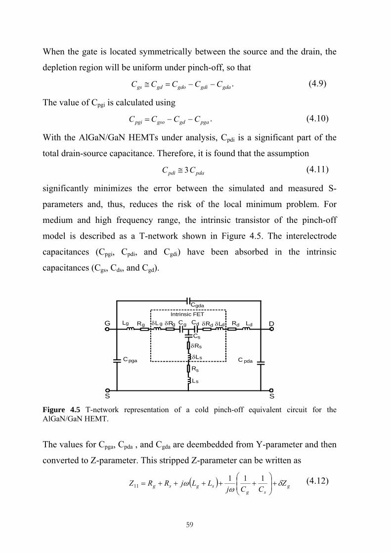
When the gate is located symmetrically between the source and the drain, the
depletion region will be uniform under pinch-off, so that
gdagdigdogdgs CCCCC −−=≅ . (4.9)
The value of Cpgi is calculated using
pgagdgsopgi CCCC −−= . (4.10)
With the AlGaN/GaN HEMTs under analysis, Cpdi is a significant part of the
total drain-source capacitance. Therefore, it is found that the assumption
pdapdi CC 3≅ (4.11)
significantly minimizes the error between the simulated and measured S-
parameters and, thus, reduces the risk of the local minimum problem. For
medium and high frequency range, the intrinsic transistor of the pinch-off
model is described as a T-network shown in Figure 4.5. The interelectrode
capacitances (Cpgi, Cpdi, and Cgdi) have been absorbed in the intrinsic
capacitances (Cgs, Cds, and Cgd).
Cgda
C pdaCpga
L
L Lg d
s
R
R
Rg d
s
C
CCg d
s
δL δL
δL
δR δR
δR
g g dd
s
s
Intrinsic FET
S S
DG
Figure 4.5 T-network representation of a cold pinch-off equivalent circuit for the AlGaN/GaN HEMT.
The values for Cpga, Cpda , and Cgda are deembedded from Y-parameter and then
converted to Z-parameter. This stripped Z-parameter can be written as
( ) gsg
sgsg ZCCj
LLjRRZ δω
ω +⎟⎟⎠
⎞⎜⎜⎝
⎛+++++=
11111
(4.12)
59

( ) dsd
sdsd ZCCj
LLjRRZ δω
ω +⎟⎟⎠
⎞⎜⎜⎝
⎛+++++=
11122
(4.13)
s
sss Z
CjLjRZZ δ
ωω +++==
1
2112 (4.14)
where
( )sgsgg LLjRRZ δδωδδδ +++= (4.15)
( )sdsdd LLjRRZ δδωδδδ +++= (4.16)
sss LjRZ ωδδδ += . (4.17)
δZg, δZd, and δZs represent correction terms related to the intrinsic parameters
of the model. Ignoring the correction terms and multiplying the Z-parameters
by ω and then taking the imaginary parts gives
[ ] ( ) ⎟⎟⎠
⎞⎜⎜⎝
⎛+−+=
sgsg CC
LLZ 11 Im 211 ωω (4.18)
[ ] ( ) ⎟⎟⎠
⎞⎜⎜⎝
⎛+−+=
sdsd CC
LLZ 11 Im 222 ωω (4.19)
Figure 4.6 Inductfor a 0.5 µm AlGa
x 1013
-1)
ance estimation from the measured cold pinched-off stripped Z-parameters N/GaN HEMT with a 2x50 µm gate width (wafer no. 398-4).
2 4 6 8 10 12 14
x 1022
-1.5
-1.4
-1.3
-1.2
-1.1
-1
-0.9
-0.8
-0.7
ω2 [rad2 s-2]
ωIm
[Z11
-Z12
], ω
Im[Z
22-Z
12], ω
Im[Z
12] (Ω
rad
s
ωLs
ωLd
ωLg
[ ]s
s CLZ 1Im 2
12 −= ωω . (4.20)
60

Hence, the values of Lg, Ld, and Ls can be extracted from the slope of Im[ωZij]
versus ω2-curve as shown in Figure 4.6. The estimated values of inductances
described above and the interelectrode capacitances (Cpgi, Cpdi, and Cgdi) are
deembedded. It is reported in [1] that the real parts of the Z-parameters in
(4.12), (4.13), and (4.14) are related to the series resistances after de-
embedding the interelectrode capacitances. Also it is reported that the
incomplete deembedding of the outer capacitances and the inductances
introduce nonlinear frequency dependence in the real part of deembedded Z-
parameters. And by multiplying the deembedded Z-parameter by ω2, this effect
is reduced. Ignoring the correction terms and multiplying the deembedded Z-
parameter by ω2 and then taking the real part of this Z-parameter gives
[ ] ( )sg RR ωZω += 211
2 Re (4.21)
[ ] ( )sd RR ωZω += 222
2 Re (4.22)
. (4.23) [ ] RωZω s2
122 Re =
0 2 4 6 8 10
0.075
0.08
0.085
0.09
Scanned C pga value [fF]
ε
Minimum Error
0 0.2 0.4 0.6 0.8 10.0739
0.074
0.0741
0.0742
Scanned Cgda value [fF]
ε
Minimum Error
0
5
10
0 0.25
0.50.75
1
0.075
0.08
0.085
0.09
Scanned Cpga value [fF]
Scanned Cgda value [fF]
ε
Minimum Error
Figure 4.7 Residual error between measured and simulated S-parameters versus Cpga and Cgda for a 0.5 µm AlGaN/GaN HEMT with a 2x50 µm gate width (wafer no. 398-4).
61

By linear regression, the value of Rg + Rs, Rd + Rs, and Rs can be extracted from
the slope of ω2Re[Zij] versus ω2 curves.
The resulting estimated parameters are used to simulate the device S-
parameters, which are then compared with the measured ones to calculate the
residual fitting error (ε) (definition see (4.33)). The outer capacitances (Cpga,
Cpda, and Cgda) are incremented, and the procedure is repeated until Cpga (Cpda)
is equal to 0.5Cdso and Cgda equal to 0.5Cgdo. The vector of model parameters
P(εmin), corresponding to the lowest error εmin, is then taken as the appropriate
starting value. Figure 4.7 shows the scanned Cpga and Cgda values and the
corresponding residual error. The arrows in this figure indicate the minimum
error and the related values of Cpga and Cgda.
Step 3) Because of unavoidable high measurement uncertainty for cold pinch-
off device, the determination of a reliable starting value for the
extrinsic resistances is difficult if not impossible [1]. Higher reliable
starting value was generated using cold gate-forward S-parameter
measurements at high gate voltage (>2.0 V). This is due to the higher
conduction band of AlGaN/GaN HEMT with respect to the
corresponding AlGaAs/GaAs HEMT [3]. Therefore, significantly
higher voltages have to be applied to reach the condition that the
influence of the intrinsic gate capacitance becomes negligible. The
determined values of extrinsic capacitances and inductances, in Step
2), are deembedded from the gate-forward measurements. The starting
values of the extrinsic resistances are then estimated from the stripped
measurements as shown in Figure 4.8.
62

2 4 6 8 10 12 14 16
x 1021
0.5
1
1.5
2
2.5x 10
23
ω2 (rad2 s-2)ω2 Re
[Z11
], ω
2 Re[Z
22], ω
2 Re[Z
12] (Ω
rad2 s
-2)
ωRs
ω(Rd+Rs)
ω(Rg+Rs)
Figure 4.8 Resistance estimation from the measured cold forward stripped Z-parameters for a 0.5 µm AlGaN/GaN HEMT with a 2x50 µm gate width (wafer no. 398-4).
Fieqno
gure 4.9 Pinchuivalent circuit . 398-4).
00.8
0.85
0.9
0.95
1
Mag
nitu
de
0-120
-100
-80
-60
-40
-20
0
Pha
se [°
]
SSMM
off S-parameter fitting with starting element values for the 22-element model of a 0.5 µm AlGaN/GaN HEMT with a 2x50 µm gate width (wafer
20 40 60Frequency [GHz]
0 20 40 600
0.1
0.2
0.3
0.4
0.5
Frequency [GHz]
Mag
nitu
de
20 40 60Frequency [GHz]
0 20 40 60-50
0
50
100
Frequency [GHz]
Pha
se [°
]
imulated S11
imulated S22
easured S11
easured S22
Simulated S11
Simulated S22
Measured S11
Measured S22
Simulated S12
Simulated S21
Measured S12
Measured S21
Simulated S12
Simulated S21
Measured S12
Measured S21
63

Complete starting values for the pinch-off device model parameters are
tabulated in Table 4.1. Good agreement between the measured and simulated
S-parameters, shown in Figure 4.9, verifies the high quality of these starting
values, particularly at low and medium frequencies.
Table 4.1: Starting values for 22-element equivalent circuit model of a 0.5-µm AlGaN/GaN HEMT with a 2 x 50 µm gate width (wafer no. 398-4).
Extrinsic Parameters Intrinsic Parameters
Cpga = 7.00 fF Cpda = 7.00 fF Cgda = 0.40 fF Cpdi = 21.00 fF Cpgi = 4.90 fF Cgdi = 0.80 fF
Lg = 39.50 pH Ld = 46.40 pH Ls = 5.25 pH Rg = 5.20 Ω Rd = 9.20 Ω Rs = 6.60 Ω
Cgs = 20.37 fF Cds = 8.47 fF Cgd = 20.01 fF Ri = 0.0 Ω Rgd = 0.0 Ω τ = 0.0 ps
Gm = 0.0 mS Gds = 0.0 mS Ggsf = 0.0 mS Ggdf = 0.0 mS
4.2.2 Model Parameter Optimization
The procedure for the generation of starting values of the model parameters
was discussed in Section 4.2.1. Here, the result of the optimized value for each
model parameter is presented. Model parameter optimization has been done
based on the principle of bidirectional optimization technique proposed by Lin
and Kompa [4]. This technique works successfully for lumped small-signal
model, but cannot be used efficiently for distributed small-signal model. This is
due to the external parasitic elements of this model, which increase the
dimension of the searching space. Now, this algorithm can be modified to
become applicable for the distributed small-signal model, where the closeness
of the generated starting value to the true value allows the searching space to be
reduced by optimizing only the extrinsic parameters. At each iteration through
the optimization process, the extrinsic parameters are assigned suitable values
and then deembedded from the measured data to determine the intrinsic Y-
parameter. The intrinsic model parameters are then estimated by means of data
64

fitting from the deembedded measurements. The whole estimated model
parameters are then used to fit the measured S-parameters. This process is
continued to find the optimal model parameters. In this case, the optimization
problem is a nonlinear multidimensional one, whose objective function is likely
to have multiple local minima. Furthermore, the cold pinch-off device
measurements have a high uncertainty [5]. These two factors increase the
probability of trapping into a local minimum. Therefore, this requires a careful
formulation for the objective function to avoid the local minima problem. The
magnitude of the error between the measured and simulated S-parameter values
can be expressed as [1]
ij
nijnijij W
SS )Im()Re( ,, δδε
+= , i,j =1,2; n =1,2,…,N (4.24)
where
ijij SW max= , i,j =1,2; i≠j (4.25)
iiii SW += 1 , i=1,2 (4.26)
and N is the total number of data points. δS is the difference between the
measured and simulated S-parameter coefficient and its simulated value. The
weighting factor Wij deemphasizes data region with higher reflection
coefficients due to the involved higher measurement uncertainty [5]. The scalar
error is then expressed as
∑=
=N
nns f
N 11)(1 εε (4.27)
where
⎥⎦
⎤⎢⎣
⎡=
)()()()(
)(2221
1211
nn
nnn ff
fff
εεεε
ε (4.28)
defined at each frequency point. However, the objective function that is based
on S-parameters alone to minimize the fitting error may not necessarly lead to
physically relevant values for the model parameters [6]. For further
65

enhancement of the objective function, another performance quantity,
depending on the final application, will be considered. The main application of
AlGaN/GaN HEMT is power amplifier design. For power amplifier design, the
output and input impedance, the device gain, and stability factor are important
for the design of matching networks. These factors can be expressed as a
function of S-parameters and fitted during the optimization. The stability factor
defined at the output plane of the device at each frequency can be expressed as
2112
*1122
2221
SSSSS
Ks +∆−
−= (4.29)
where S* is the complex conjugate and ∆s is the determinant of S-parameter
matrix at each frequency [7]. The fitting error of the stability factor is given by
∑=
−=N
ksimmeasK KK
N 1
1ε (4.30)
where Kmeas and Ksim are the stability factors from the measured and simulated
S-parameters, respectively. With regard to the device gain, the maximally
efficient gain defined in [8] is a more suitable one, since it remains finite even
for an unstable device. This gain may be defined at each frequency as
221
221
ln
1
S
SG
−= . (4.31)
The error in the gain may, thus, be expressed as
∑=
−=N
msimmeasG GG
N 1
1ε (4.32)
where Gmeas and Gsim are the gains computed from the measured and modeled
S-parameters. The fitting error can be defined in terms of the three error
components as
( )222
31
GKs εεεε ++= . (4.33)
66

The modified Simplex optimization algorithm proposed in [6] is used to
minimize the objective function in (4.33). The optimized device parameters are
listed in Table 4.2.
Table 4.2: Optimized pinch-off device parameters of a 0.5 µm AlGaN/GaN HEMT with a 2x50 µm gate width (wafer no. 398-4).
Extrinsic Parameters Intrinsic Parameters
Cpga = 9.97 fF Cpda = 7.13 fF Cgda = 0.47 fF Cpdi = 29.42 fF Cpgi = 7.09 fF Cgdi = 0.86 fF
Lg = 46.55 pH Ld = 47.90 pH Ls = 6.25 pH Rg = 4.80 Ω Rd = 11.80 Ω Rs = 5.47 Ω
Cgs = 15.38 fF Cds = 0.0 fF Cgd = 20.17 fF Ri = 0.0 Ω Rgd = 0.0 Ω τ = 0.0 ps
Gm= 0.0 mS Gds= 0.0 mS Ggsf = 0.0 mS Ggdf = 0.0 mS
4.3 Intrinsic Parameter Extraction
After deembedding the extracted extrinsic parameters in Section 4.2, the bias-
dependent intrinsic parameters can be extracted. Figure 4.10 shows the
extracted intrinsic capacitances and conductances, at VGS = -1 V and VDS = 10
V in the saturation region, versus frequency. The frequency independency of
the intrinsic elements, especially in the low and medium frequency range,
verifies the validity of the proposed small-signal model topology and the
developed extraction method. However, the frequency-dependent effect in the
intrinsic elements, especially for bias condition in the linear region, cannot be
ignored. This effect reduces the reliability of intrinsic parameter extraction. To
account for this effect, an efficient technique is developed for extraction of the
optimal value for the intrinsic element. In this technique, the intrinsic Y-
parameters are formulated in a way where the optimal intrinsic element value
can be extracted using simple linear data fitting.
67

250
Figure 4.10 ExtracV and VDS = 10 V398-4).
The admittance o
By defining a ne
Cgs can be deter
fitting, where ω
Ri can be determ
fitting. Ggsf can
the megahertz ra
given by
0 10 20 30 40 50 600
50100150200
Cgs
, C
gd (f
F)
0 10 20 30 40 50 600
10
20
30
40
Frequency (GHz)
Gm
, G
ds (
mS)
Cgs
Cgd
Gm
Gds
ted intrinsic capacitances and conductances versus frequency at VGS = -1 for a 0.5 µm AlGaN/GaN HEMT with a 2x50 µm gate width (wafer no.
f the intrinsic gate-source branch Ygs is given by
gsigsfi
gsgsfiigs CRjGR
CjGYYY
1
12,11, ωω
+++
=+= . (4.34)
w variable D as
gsgs
gsf
gs
gs CC
GY
YD
]Im[
22
ωω
+== (4.35)
mined from the slope of the curve for ωD versus ω2 by linear
is the angular frequency. By redefining D as
jCRC
GRGY
YD gsi
gs
gsfigsf
gs
gs −++
==
)1(]Im[
ωω
(4.36)
ined from the plot of the real part of ωD versus ω2 by linear
be determined from the real part of Ygs at low frequencies (in
nge). The admittance for the intrinsic gate-drain branch Ygd is
gdgdgdfgd
gdgdfigd CRjGR
CjGYY
1
12, ωω
+++
=−= . (4.37)
68
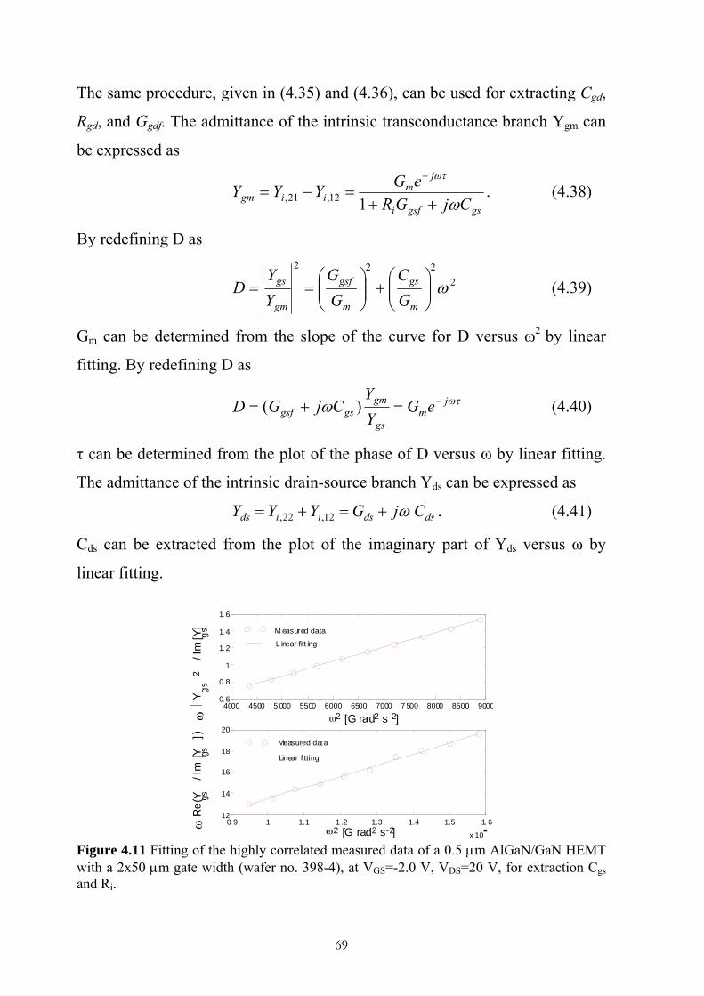
The same procedure, given in (4.35) and (4.36), can be used for extracting Cgd,
Rgd, and Ggdf. The admittance of the intrinsic transconductance branch Ygm can
be expressed as
gsgsfi
jm
iigm CjGReGYYY
ω
ωτ
++=−=
−
112,21, . (4.38)
By redefining D as
2222
ω⎟⎟⎠
⎞⎜⎜⎝
⎛+⎟⎟
⎠
⎞⎜⎜⎝
⎛==
m
gs
m
gsf
gm
gs
GC
GG
YY
D (4.39)
Gm can be determined from the slope of the curve for D versus ω2 by linear
fitting. By redefining D as
ωτω jm
gs
gmgsgsf eG
YY
CjGD −=+= )( (4.40)
τ can be determined from the plot of the phase of D versus ω by linear fitting.
The admittance of the intrinsic drain-source branch Yds can be expressed as
dsdsiids CjGYYY 12,22, ω+=+= . (4.41)
Cds can be extracted from the plot of the imaginary part of Yds versus ω by
linear fitting.
4000 4500 5 000 5500 6000 6500 7000 7 500 8000 8500 90000. 6
0. 8
1
1. 2
1. 4
1. 6
ω2 [G rad2 s-2]
Y gs
2
/ Im
[Y gs]
0. 9 1 1.1 1 .2 1.3 1.4 1.5 1. 6
x 10
12
14
16
18
20
ω2 [G rad2 s-2]
Re(
Y gs /
Im [Y gs
])
M easured data
L inear fitt ing
Measured dat a
Linear fitting
ωω
Figure 4.11 Fitting of the highly correlated measured data of a 0.5 µm AlGaN/GaN HEMT with a 2x50 µm gate width (wafer no. 398-4), at VGS=-2.0 V, VDS=20 V, for extraction Cgs and Ri.
69

0 5 10 15 20 25
-6-4-2020
50100
170
VDS (V) VGS (V)
Cgs
(fF
)
0 5 10 15 20 25
-6-4
-202
0100200300370
VDS (V) VGS (V)
Cgd
(fF
)
0 5 10 15 20 25
-6-4-2
020
10
20
32
VDS (V) VGS (V)
Gm
(mS)
0 5 10 15 20 25
-6-4-2
020
100200300
450
VDS (V) VGS (V)
Ggs
(m
S)
Figure 4.12 Extracted Cgs, Cgd, Gm, and Gds as a function of the extrinsic voltages for a 0.5 µm AlGaN/GaN HEMT with a 2x50 µm gate width (wafer no. 398-4).
Figure 4.13 Extracted Ri, τ, Ggsf, and Ggdf as a function of the extrinsic voltages for a 0.5 µm AlGaN/GaN HEMT with a 2x50 µm gate width (wafer no. 398-4).0 5 10 15 20 25
-6-4
-20
20
10
20
VDS (V) VGS (V)
Ri ( Ω
)
0 5 10 15 20 25
-6-4
-20
20
5
10
VDS (V)VGS (V)
τ (p
s)
0 5 10 15 20 25
-6-4
-20
20
50
100
VDS (V) VGS (V)
Ggs
f (m
S)
0 5 10 15 20 25
-6-4
-20
20
20
40
VDS (V) VGS (V)
Ggd
f (mS)
70

Due to the frequency-dependent effect in the output conductance, Gds is
determined from the curve of ωRe[Yds] versus ω by linear fitting. Further
refinement can be done by using only the more linear part of the curves, instead
of the whole range, for optimal extraction of the intrinsic parameters. A
searching procedure for determining the more linear part of the curves is
developed. This procedure is based on the correlation coefficient as a measure
to define the more linearly correlated data range. Intrinsic parameter extraction
using the proposed procedure gives an accurate determination for the intrinsic
element value even for significant frequency dependency of this element.
Figure 4.11 shows the results of optimal frequency range determination for
extracting Cgs and Ri. Figures 4.12, 4.13, and 4.14 present the extracted
intrinsic parameters versus the extrinsic bias voltages. The extraction results
show the typical expected characteristics of the AlGaN/GaN HEMT.
0 5 10 15 20 25
-6-4
-20
20
10
20
32
VDS (V)VGS (V)
Rgd
( Ω)
0 5 10 15 20 25
-6-4
-20
20
100200300
450
VDS (V)VGS (V)
Cds
(fF
)
Figure 4.14 Extracted Rgd and Cds as a function of the extrinsic voltages for a 0.5 µm AlGaN/GaN HEMT with a 2x50 µm gate width (wafer no. 398-4).
From the device physics point of view, Cgs appears as a parallel-plat
capacitance whose two plates are formed by the gate metal and the 2DEG
channel charge [16]. The effective seperation of this capacitor is determined by
the depletion layer depth under the gate, which extends all the way to
heterojunction at high negative gate voltage. Therefore, rapid decrease for Cgs
can be noted in Figure 4.12 in the pinch-off region (VGS ≤ -4 V). The lateral
71

electric field established by the drain voltage, accelerates charge carriers in the
channel to scatter into the barrier layers. This results in reduction of the
depletion layer depth, and therefore gradual increase for Cgs with increasing the
drain voltage is observed around the grounded gate voltage (VGS = 0 V). Cgd
capacitance is originated in the extension of the depletion region into the gate-
drain space. This extension increases with increasing drain voltage. Therefore,
smaller values for Cgd is obtained with increasing drain voltage, as shown in
Figure 4.12. As can also be seen in this figure, Cgd increases rapidly with
increasing gate voltage under low drain voltage conditions. Under these
conditions the depletion region is diminished and uniformly distributed under
the gate. Therefore, the gate capacitance can be splitted into two approximately
equal capacitances, Cgd and Cgs. Gm is related to the channel charge density and
electron velocity. These two factors are mainly controlled by the gate and drain
voltage, respectively. Therefore, significant increase for Gm can be seen in
Figure 4.12 with increasing gate voltage. Due to the linear variation of the
electron velocity under low electric field strengths along the channel [10], Gm
increases linearly with increasing drain voltage in the ohmic region (VDS < 5
V). In the saturation region (VDS > 5 V), Gm becomes constant as the electron
velocity saturates at higher channel electric field. Physically, Gds models the
variation of the drain current with the drain voltage. Thus, small values for Gds
in the saturation region can be observed in Figure 4.12. Increasing the gate
voltage increases the channel charge density and thus the drain current. This
increase becomes remarkable in the ohmic region due the reduction of the
depletion layer. Therefore, corresponding increase for Gds can be noted in this
region with increasing the gate voltage. Ri models the undepleted part (low
field region) of the channel under the gate, through which the gate-source
capacitance is charged. The value of Ri is equal to the ratio of the potential
drop in this channel part and the channel current, which is approximately equal
to the drain current [10]. Therefore, it is expected that the value of Ri should be
72

high in the low drain current region as shown in Figure 4.13. From the physics
point of view, τ is argued to equal the transit time of electrons in the channel
under the depletion region [10]. Extension of the depletion region in the gate-
drain area, due to an increase of the drain-gate voltage, increases the required
transit time for the electron. Therefore, τ is expected to be increased with
increasing drain voltage or decreasing gate voltage, as can be observed in
Figure 4.13. Ggsf and Ggdf model the conduction current through the gate-
source and gate-drain Schottky diodes. Therefore, they have large values only
when the gate voltage is beyond the diodes turn on voltage (VGS ≈ 1.5 V), as
can be seen in Figure 4.13. Charging resistance Rgd is included in the model
mainly to simulate the symmetrical distribution of the depletion region under
the gate in the ohmic-forward region (VDS < 5 V and VGS > 0 V). Therefore, it
is expected that Rgd should have the same behavior as Ri in this region, as
shown in Figure 4.14. The physical origin of Cds can be attributed to the high-
field part of the depletion layer, which separates the source and drain electrodes
in an electrostatic sense [16]. Therefore, higher values for Cds will be obtained
in the ohmic region, due to the reduction of the high-field part, as can be shown
in Figure 4.14.
4.4 Small-Signal Model Verification
4.4.1 S-Parameter Simulation
The small-signal modeling is verified through the simulation of the S-
parameter for the analyzed 2x50-µm device. Figure 4.15 shows the results of S-
parameter simulation at different bias points, in linear and saturation regions,
over a wide frequency range. Very good agreement is achieved between
measurements and simulations. Bias-dependent S-parameter simulation, for the
73
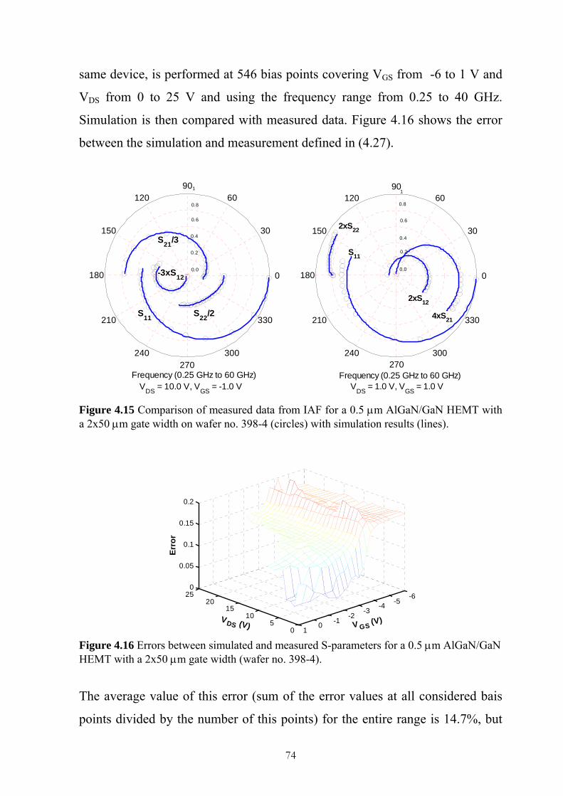
same device, is performed at 546 bias points covering VGS from -6 to 1 V and
VDS from 0 to 25 V and using the frequency range from 0.25 to 40 GHz.
Simulation is then compared with measured data. Figure 4.16 shows the error
between the simulation and measurement defined in (4.27).
190
Fa
FH
T
p
190
0.2
0.4
0.6
0.8
30
210
60
240270
120
300
150
330
180 0-3xS12
S21/3
S22/2 S11
Frequency (0.25 GHz to 60 GHz)
0.0
VDS = 10.0 V, VGS = -1.0 V
0.2
0.4
0.6
0.8
30
210
60
240270
120
300
150
330
180 00.0
Frequency (0.25 GHz to 60 GHz)
2xS22
2xS12
4xS21
S11
VDS = 1.0 V, VGS = 1.0 V
igure 4.15 Comparison of measured data from IAF for a 0.5 µm AlGaN/GaN HEMT with 2x50 µm gate width on wafer no. 398-4 (circles) with simulation results (lines).
igure 4.16 ErrorEMT with a 2x5
he average va
oints divided
05
1015
2025 -6
-5-4-3
-2-10
1
0
0.05
0.1
0.15
0.2
V GS (V) VDS (V)
Err
or
s between simulated and measured S-parameters for a 0.5 µm AlGaN/GaN 0 µm gate width (wafer no. 398-4).
lue of this error (sum of the error values at all considered bais
by the number of this points) for the entire range is 14.7%, but
74

its average value in the linear and saturation, excluding the pinch-off, regions is
10%. These results also validate the proposed small-signal model over a wide
bias range.
The intrinsic transient frequency fT is computed based on the extracted intrinsic
transconductance and intrinsic gate capacitances using the following expression
[10]
)( 2 gdgs
mT CC
Gf+
=π
. (4.42)
Figure 4.17 shows fT as a function of extrinsic gate-source and drain-source
voltages. The value of fT is nearly constant versus drain-source voltage in
saturation region, which is one of the most important advantages of
AlGaN/GaN HEMT for high power applications.
Figure 4.17 Varivoltages for a 0.5
4.4.2 Physica
The effective g
05
1015
2025
-6-4
-20
0
5
10
15
20
25
30
V DS (V) VGS (V)
fT
(GH
z)
ation of the calculated intrinsic transient frequency with the extrinsic bias µm AlGaN/GaN HEMT with a 2x50 µm gate width (wafer no. 398-4).
l Validation
ate length of AlGaN/GaN HEMT is defined in [9] as
δσ ++= (4.43) Geff LL
75

where σ describes the symmetrical increase in the physical gate length at low
drain-source voltage. δ accounts for the extension of the depletion region,
which increases with increasing drain-gate electric field. As a physical
validation of the extraction results, the effective gate length is computed using
the formula [10]
T
sateff f
vLπ2
= (4.44)
where vsat is the electron saturation velocity. The measured vsat, for
AlGaN/GaN HEMT, has a maximum value of 1.1 x 107 cm/s [9], [11]. Using
this value, Leff is calculated over a wide bias point range as shown in Figure
4.18. The large values of Leff in the ohmic region can be corrected by taking
into account the bias dependence of vsat, which shows lower values in this
region [9]. Leff variation in the saturation region (>5V) is between 0.63 and 0.86
µm. These values are comparable with the expected values for this device
assuming that the extreme variation of Leff, in saturation region, is between
1.25LG and 2LG [10]. This consistency confirms the physical validity of the
extracted small-signal model paramer values obtained for AlGaN/GaN HEMT
using our developed approach.
05
1015
2025
-3
-2
-1
00.50.70.91.11.31.51.71.9
VDS (V) VGS (V)
Lef
f ( µ
m)
Figure 4.18 Calculated effective gate length as function of extrinsic bias voltages VGS and VDS for a 0.5 µm AlGaN/GaN HEMT with a 2x50 µm gate width (wafer no. 398-4).
76

4.5 Small-Signal Model Scaling
As mentioned in Section 4.2, the required measurement frequency range for
reliable extraction of the distributed small-signal model parameters is 60 GHz
for a 2x50-µm device. However, this frequency range reduces to 20 GHz for a
1-mm device and becomes smaller for larger devices. This can also be noted by
comparing the pinch-off S-parameter measurements of different sizes of the
AlGaN/GaN HEMTs as shown in Figure 4.19. Regarding the traces, as can be
seen in this figure, the measurements of 4-mm device, in the 5 GHz range, have
strong similarity with 1-mm device characteristics. In this case one can
conclude that the optimal extraction frequency range for 4-mm device may also
decrease to around 5 GHz.
Figure 4.19 Pinch-off S-parameter measurements from IAF for 16x250 µm and 8x125 µm gate width AlGaN/GaN HEMTs (wafer no. 707-4).
0 5 10 15 200.7
0.8
0.9
1
Mag
nitu
de
0 5 10 15 20
0.1
0.2
0.3
0.4
0.5
Mag
nitu
de
0 5 10 15 20150
200
250
300
350
F [GHz]
Phas
e [°
]
0 5 10 15 20-130
-70
0
80
F [GHz]
Pha
se [°
]
S11 S22 S11 S22 S21 S12 S21 S12
4-mmGaNHEMT
1-mm GaN HEMT
4-mm GaN HEMT
1-mm GaN HEMT
1-mm GaN HEMT
4-mm GaN HEMT
4-mmGaNHEMT
1-mm GaN HEMT
77

To verify this observation, the model parameter extraction was performed
using different frequency ranges, for different device sizes. Thus, depending on
the reliability of the extracted model parameters, the optimal frequency can be
determined. As expected, there is remarkable decrease for the optimal
extraction frequency range by increasing the device gate width as shown in
Figure 4.20. The physical origin of this behavior is the small-signal model
limitation with respect to signal frequency. The total gate width of the device is
increased with increasing the unit gate width or the number of fingers. The
latter one defines the metal interconnection length. If the unit gate width or the
interconnection length become too large with respect to the signal wavelength,
these elements act as transmission line segments. In this case the model cannot
describe the device, and the signal frequency should be decreased.
Figure 4.20 Optimal frequency range for reliable model parameter extraction.
0 1 2 3 40
10
20
30
40
50
60
70
Gate Width (mm)
Opt
imal
Fre
quen
cy R
ange
(GH
z)
The model parameter extraction results for 1-mm, 2-mm, and 4-mm gate width
devices using the determined optimal frequency range are tabulated in Table
4.3. As shown in this table, the extracted pad capacitances (Cpga, Cpda, and Cgda)
are in proportion with the gate width. There is no significant difference
between the pad capacitances of 8x125-µm and 8x250-µm devices because the
pad connection area is related mainly to the number of fingers. The
interelectrode capacitances (Cpdi and Cgdi) are also in proportion with the gate
78

width. Due to the small values of Rg and Rs, for larger devices, Cpgi cannot be
separated completely from the intrinsic capacitance (Cgs).
Table 4.3: Extracted model parameters for different device sizes on wafer no. 707-4 under
pinch-off bias condition (VDS = 0 V and VGS = Vpinch-off).
Parameter Wg = 16x250 µm Wg = 8x250 µm Wg = 8x125 µm
Cpga (fF) Cpgi (fF) Cgs (fF)
233.5 39.6 1508.4
89.8 234.8 538.6
86.9 332.2 255.8
Cgda (fF) Cgdi (fF) Cgd (fF)
121.6 265.6 1285.7
41.7 96.5 757.8
0.0 0.0 517.4
Cpda (fF) Cpdi (fF) Cds (fF)
206.4 790.7 0.0
90.9 390.2 0.0
86.3 245 1.0
Lg (pH) Ld (pH) Ls (pH)
122.3 110.9 3.6
81.9 75.4 5.7
57.3 54.5 5.6
Rg (Ω) Rd (Ω) Rs (Ω)
1.1241 0.71424 0.25152
2.8 1.4 0.5
1.7 2.3 0.9
Ri (Ω) Rgd (Ω)
0.0 0.1
0.0 0.0
0.0 0.0
Gm (mS) τ (ps) Gds (mS)
0.0 0.0 0.34
0.0 3.3 0.0
0.0 0.0 0.26
Ggsf (mS) Ggdf (mS)
2.3 0.24
0.6 0.25
0.4 0.2
However, the sum of Cpgi and Cgs is in proportion with the gate width. By direct
scaling of the 8x250-µm device, the expected values of Cgda and Cgdi for 8x125-
µm device are 20 fF and 40 fF, respectively. Due to the smaller values of these
elements and also due to the smaller values of Lg and Ld for this device, Cgda
and Cgdi cannot be separated form Cgd, which is very large at pinch-off. The
parasitic inductance includes the self-inductance due the metalisation contact
and the mutual inductance between the metal interconnection, which increases
by increasing the number of fingers. For this reason, there is a significant
79

increase of Ld and Lg values for 16x250-µm device with respect to 8x125-µm
device. The parasitic resistances (Rd and Rs) are inversely proportional with the
gate width. However, this is not the case for Rg, which is proportional with the
unit gate width and inversely proportional with the number of gate fingers [12],
[13].
Table 4.4: Intrinsic model parameters for different device sizes on wafer no. 707-4 under
active bias condition (VGS = -2 V and VDS = 21 V).
Parameter Wg = 16x250 µm Wg = 8x250 µm Wg = 8x125 µm
Cgs (pF) Cgd (pF) Cds (pF)
7.06 0.23 0.22
3.61 0.18 0.03
1.99 0.17 0.0
Ri (Ω) Rgd (Ω) τ (ps)
0.44 36.6 2.3
0.39 27.3 2.53
0.0 4.9 2.24
Gm (mS) Gds (mS)
1009.19 21.0
541.1 12.92
327.3 5.64
Ggsf (mS) Ggdf (mS)
9.76 1.98
2.13 0.46
1.82 0.28
After deembedding the extracted extrinsic parameters in Table 4.3, the bias-
dependent intrinsic parameters for the active device under considered bias
conditions can be extracted. The intrinsic parameters of an active device for
different gate widths are presented in Table 4.4. As noted, the main nonlinear
elements (Cgs, Gm, Gds, Ggsf, and Ggdf) values are directly proportional to the
gate width. In saturation region the value of Cgd and Ri are not large enough to
show significant proportionality. Rgd is proportion with the gate width, which is
in agreement with reported observation in [14]. The small signal modeling of
the investigated devices is verified through the S-parameter simulation. Figure
4.21, Figure 4.22 and Figure 4.23 show the results of S-parameter simulation at
different bias points, in saturation and ohmic regions, compared with
measurement. The model can accurately simulate the S-parameter
measurement. Also it can predict the kink effect in S22, which occurs in larger
80

size FETs and related to the frequency dependence of the device output
impedance [12].
0.2
0.4
0.6
0.8
1
30
210
60
240
90
270
120
300
150
330
180 0
S22
S11
0.08xS21
5xS12
Frequency from 0.5 to 20 GHz VGS = -1.0 V, VDS = 25.0 V
0.2
0.4
0.6
0.8
1
30
210
60
240
90
270
120
300
150
330
180 0
S11
S22 -5xS12
2xS21
Frequency from 0.5 to 20 GHz VGS = 1.0 V, VDS = 3.0 V
(a) (b) Figure 4.21 Comparison of measured (circles) and simulated (lines) S-parameter for a 8x125-µm AlGaN/GaN HEMT on wafer no. 707-4 under bias condition in: (a) saturation region and (b) ohmic region.
0.2
0.4
0.6
0.8
1
30
210
60
240
90
270
120
300
150
330
180 0
0.05xS21
10xS12 S22
S11
Frequency from 0.5 to 15 GHz VGS = -1.5 V, VDS = 15 V
0.2
0.4
0.6
0.8
1
30
210
60
240
90
270
120
300
150
330
180 0
-S11
S22
10xS12
0.2xS21
Frequency from 0.5 to 15 GHz VGS = -2.0 V, VDS = 1.0 V
(a) (b)
Figure 4.22 Comparison of measured (circles) and simulated (lines) S-parameter for a 8x250-µm AlGaN/GaN HEMT on wafer no. 707-4 under bias condition in: (a) saturation region and (b) ohmic region.
81

Figure 4.23 Comparison of measured (circles) and simulated (lines) S-parameter for a 16x250-µm AlGaN/GaN HEMT on wafer no. 707-4 under bias condition in: (a) saturation region and (b) ohmic region.
References
[1] W. Mwema, “A reliable optimisation-based model parameter extraction approach for GaAs-based FETs using measurement-correlated parameter starting values,” Doctoral Thesis, Department of High Frequency Engineering, University of Kassel, Kassel, Germany, 2002.
[2] J. A. Nelder and R. Mead, “A simplex method for function minimisation,” Computer Journal, vol. 7, pp. 308-313, 1965.
[3] R. Gaska, J. W. Yang, A. Osinsky, A. D. Bykhovski, and M. S. Shur, “Piezoeffect and gate current in AlGaN/GaN high electron mobility transistors”, Appl. Phys. Lett., vol.71 , pp. 3673-3675, December 1997.
Frequency from 0.5 to 10 GHzVGS = -2.0 V, VDS = 21.0 V
0.2
0.4
0.6
0.8
1
30
210
60
240
90
270
120
300
50
330
0.1xS21
10xS12
S22
S11 S22
0.2
0.4
0.6
0.8
1
30
210
60
240
90
270
120
300
150
330
180 0
0.5xS21
10xS12
S11 -S22
Frequency from 0.5 to 10 GHz VGS = 1.0 V, VDS = 5.0 V
(a) (b)
[4] F. Lin and G. Kompa, “FET model parameter extraction based on optimization with multiplane data-fitting and bidirectional search—a new concept,” IEEE Trans. Microw. Theory Tech., vol. 42, pp. 1114-1121, July 1994.
[5] System manual HP8510B network analyzer, HP Company, Santa Rosa, CA, Jul. 1987, P/N 08510-90074.
[6] G. Kompa and M. Novotny, “Frequency-dependent measurement error analysis and refined FET model parameter extraction including bias-dependent series resistors,” in Int. IEEE Experimentally Based FET Device Modeling and Related Nonlinear Circuit Design Workshop, Kassel, Germany, pp. 6.1-6.16, July 1997.
82

[7] M. Edwards and J. Sinsky, “A new criterion for linear two-port stability using a single geometrically derived parameter,” IEEE Trans. Microw. Theory Tech., vol. 40, pp. 2303-2311, December 1992.
[8] K. Kotzebue, “Maximally efficient gain: a figure of merit for linear active 2-ports,” Electron. Lett., vol. 12, pp. 490-491, September 1976.
[9] C. Oxley and M. Uren, “Measurements of unity gain cutoff frequency and saturation velocity of a GaN HEMT transistor,” IEEE Trans. Electron Devices, vol. 52, pp. 165-169, February 2005.
[10] P. Ladbrooke, MMIC design GaAs FETs and HEMTs. Norwood, MA: Artech House, 1988.
[11] C. Oxley, M. Uren, A. Coates, and D. Hayes, “On the temperature and carrier density dependence of electron saturation velocity in an AlGaN/GaN HEMT,” IEEE Trans. Electron Devices, vol. 53, pp. 565-567, March 2006.
[12] Ravender Goyal, Monolithic Microwave Integrated Circuit: Technology & Design. Norwood, MA: Artech House, 1989.
[13] J. Michael Golio, Microwave MESFETs & HEMTs. Norwood, MA: Artech House, 1989.
[14] M. Novotny and G. Kompa, “Scaling of FETs using the multi-bias extraction procedure,” International IEEE Workshop on Experimentally Based FET Device Modelling & Related Nonlinear Circuit Design, University of Kassel, Kassel, Germany, pp. 46.1-46.3, July 1997.
[15] S. S. Lu, C. Meng, T. W. Chen, and H. C. Chen, “The origin of the kink phenomenon of transistor scattering parameter S22,” IEEE Trans. Microw. Theory Tech., vol. 49, pp. 333-340, February 2001.
[16] H. Rohdin, A. Nagy, V. Robbins, C.-Y. Su, A. S. Wakita, J. Seeger, T. Hwang, P. Chye, P. E. Gregory, S. R. Bahl, F. G. Kellert, L. G. Studebaker, D. C. D’Avanzo, and S. Johnsen, “0.1-µm gate-length AlInAs/GaInAs/GaAs MODFET MMIC process for applications in high-speed wireless communications,” Hewlett-Packard Journal, vol. 49, pp. 1-37, February 1998.
83

Chapter 5
AlGaN/GaN HEMT Large-Signal Modeling
In this chapter, a large-signal model for AlGaN/GaN HEMT will be presented.
This model is derived from the physically relevant distributed small-signal
model described in the last chapter. First, the large-signal model equivalent
circuit will be described. Next, procedure of the model element extraction will
be explained. And then, the model implementation in ADS will be shown.
Finally, the model verification through comparison of small-signal and large-
signal simulations with measurements will be presented.
5.1 Large-Signal Model Equivalent Circuit
The developed large-signal model equivalent circuit for AlGaN/GaN HEMT is
shown in Figure 5.1. In this circuit, two quasi-static gate current sources, Igs and
Igd, and two quasi-static gate charge sources, Qgs and Qgd, are used to describe
the conduction and displacement currents. The nonquasi-static effect in the
channel charge is approximately modeled with two bias-dependent resistances,
Ri and Rgd, in series with Qgs and Qgd, respectively. As explained in Chapter 3,
this implementation improves the model simulation at millimeter wave
frequencies by taking into account the required charging times for the depletion
region capacitances. These charging times are described implicitly in the model
by RiCgs and RgdCgd products. A nonquasi-static drain current model accounts for
trapping and self-heating effects is embedded in the proposed large-signal
model. The drain current value is determined by the applied intrinsic voltages,
84

Vgs and Vds, while the amount of trapping induced current dispersion is
controlled with the RF components of these intrinsic voltages.
Figureeffects
These
circui
and C
mode
are al
or fro
gate a
and R
equiv
accura
This f
and o
5.1 Large-signal model for AlGaN/GaN HEMT including self-heating and trapping .
Vgs Vds
g d
s s
+
+
Q V Vgs gs ds( , )I V Vgs gs ds( , )
Q V Vgd gs ds( , )
I V Vgd gs ds( , )
R V Vi( , )gs ds
R V Vgd( , )gs ds
I V Vds gs ds( , ),V ,Vgso dso, T∆
CDT
RDT
CGT
RGT ( )V Vds dso - ( )V Vgs gso -
∆TRthCth
R = 1 th Ω
Vds dsI
components are extracted from the intrinsic voltage using RC high-pass
ts in the gate and drain sides as shown in Figure 5.1. The capacitors, CGT
DT values, are selected in the order of 1 pF to provide a “macroscopic”
ling of small stored charges in the surface and buffer traps. These charges
most related to the leakage currents from the gate metal edge to the surface
m the channel into the buffer layer [2]. The small leakage currents in the
nd drain paths are realized with large (in order of 1 MΩ) resistances RGT
DT in series with CGT and CDT, respectively. This implementation makes the
alent circuit more physically meaningful; also it improves the model
cy for describing the low frequency dispersion as shown in Figure 5.2.
igure shows simulated frequency dispersion in channel transconductance
utput conductance, which is related mainly to the surface and buffer traps.
85
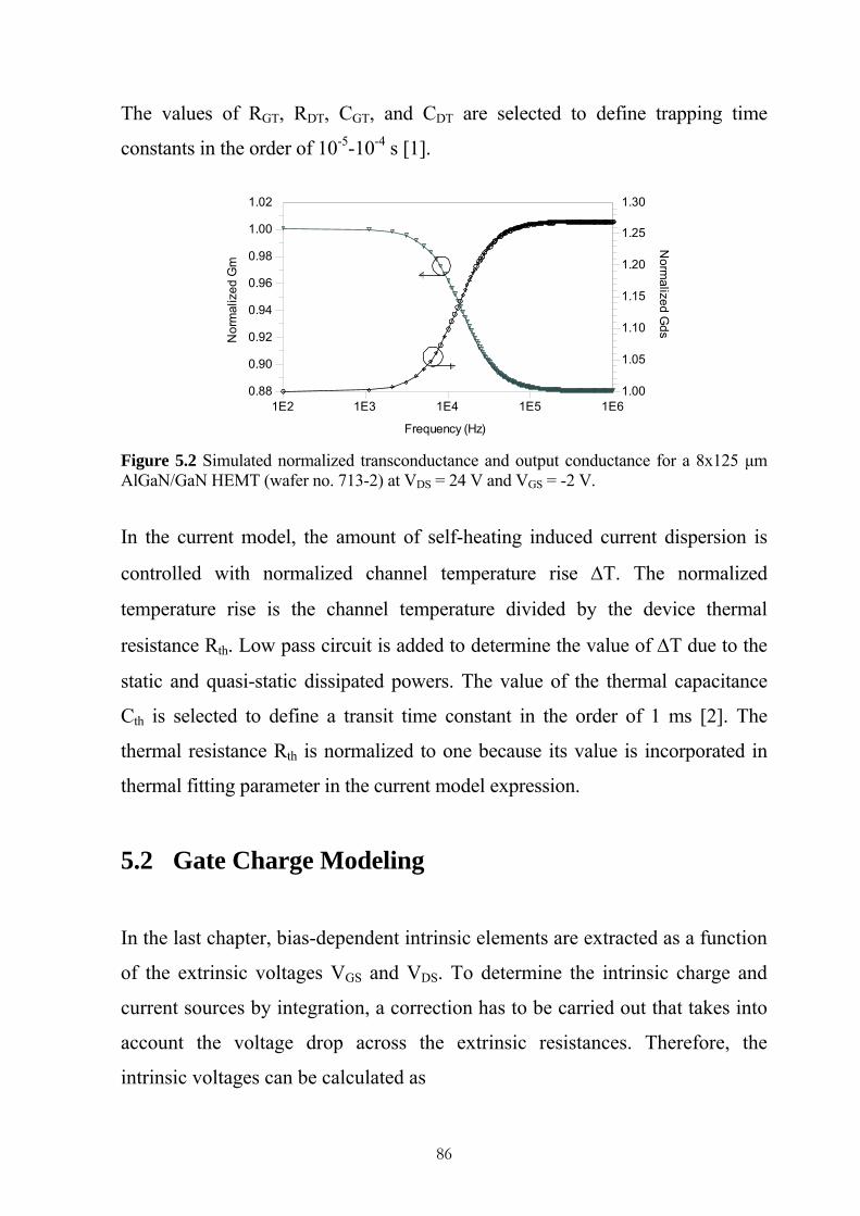
The values of RGT, RDT, CGT, and CDT are selected to define trapping time
constants in the order of 10-5-10-4 s [1].
1.02 1.30
Figure 5.2 SiAlGaN/GaN H
In the curre
controlled
temperature
resistance R
static and q
Cth is selec
thermal resi
thermal fitti
5.2 Gat
In the last c
of the extri
current sour
account the
intrinsic vol
1E3 1E4 1E51E2 1E6
0.90
0.92
0.94
0.96
0.98
1.00
0.88
1.05
1.10
1.15
1.20
1.25
1.00
Frequency (Hz)
No
rma
lized
Gd
s
No
rma
lize
d G
m
mulated normalized transconductance and output conductance for a 8x125 µm EMT (wafer no. 713-2) at VDS = 24 V and VGS = -2 V.
nt model, the amount of self-heating induced current dispersion is
with normalized channel temperature rise ∆T. The normalized
rise is the channel temperature divided by the device thermal
th. Low pass circuit is added to determine the value of ∆T due to the
uasi-static dissipated powers. The value of the thermal capacitance
ted to define a transit time constant in the order of 1 ms [2]. The
stance Rth is normalized to one because its value is incorporated in
ng parameter in the current model expression.
e Charge Modeling
hapter, bias-dependent intrinsic elements are extracted as a function
nsic voltages VGS and VDS. To determine the intrinsic charge and
ces by integration, a correction has to be carried out that takes into
voltage drop across the extrinsic resistances. Therefore, the
tages can be calculated as
86

( ) gssdssdDSds IRIRRVV −+−= (5.1)
( ) dssgssgGSgs IRIRRVV −+−= . (5.2)
This implies that the values of the intrinsic voltages Vgs and Vds are no longer
equidistant, which makes the intrinsic elements integration difficult to achieve.
Also this representation is not convenient to handle in ADS simulator.
Interpolation technique can be used to redistribute the intrinsic element data
uniformly with respect to the intrinsic voltages. However, the main limitations of
this technique are that it produces discontinuities and almost oscillating behavior
in the interpolated data. These effects result in inaccurate simulation of higher
order derivatives of the current and charge sources, which deteriorate output
power harmonics and intermodulation distortion simulations [3]. Therefore, B-
spline approximation technique is used for providing a uniform data for the
intrinsic elements. In this technique, polynomial basis functions of degree k are
used to force fitting curve to pass through the fitted data in a smooth manner
[16]. Therefore it can maintain the continuity of the data and its higher
derivatives up to (k-1)th derivative. Figure 5.3 shows equidistant fitted data, for
the intrinsic transconductance and gate-source capacitance, using cubic B-spline
approximation.
-6 -5 -4 -3 -2 -1 0-3
-2
-1
0
1
2
3
Vgs (V)
Cgs
(pF
), C gs
2 (pF
/V),
C gs3 (
pF/V
2 )
Cgs
Cgs2Cgs3
-6 -5 -4 -3 -2 -1 0-600
-400
-200
0
200
400
600
800
Vgs (V)
Gm
(m
S), G
m2 (m
S/V
), G m
3 (m
S/V2 )
GmGm2Gm3
Figure 5.3 Extracted intrinsic gate capacitance and channel transconductance and their higher derivatives at Vds = 10 V for a 8x125 µm gate width AlGaN/GaN HEMT (wafer no. 713-2).
87

As shown in the figure, this approximation technique preserves the continuity of
the data and its derivatives up to the 2nd derivative. Thus, this will improve the
model simulation for the harmonics and the intermodulation distortions [4], [17].
The intrinsic capacitances Cgs, Cgd, and Cds are integrated using (3.8) and (3.9) to
determine the values of Qgs and Qgd. The shapes of Qgs and Qgd, shown in Figure
5.4, for AlGaN/GaN HEMT are similar to the reported ones for AlGaAs/GaAs
HEMT in [5]. The determined values of Qgs and Qgd, which have an orthogonal
set of Vgs and Vds, can simply be written in CITI-file format for implementation
in ADS as a table-based model.
05
1015
20
-6-4
-20
2-1
1
3
5
7
Vds (V) Vgs (V)
Qgd
(pC
)
05
1015
20
-6-4
-20
20
3
6
9
Vds (V) Vgs (V)
Qgs
(pC)
Figure 5.4 Calculated gate charge sources Qgs and Qgd versus intrinsic voltages for a 8x125 µm gate width AlGaN/GaN HEMT (wafer no. 713-2).
5.3 Gate Current Modeling
The gate currents Igs and Igd are determined by integration the intrinsic gate
conductances Ggsf and Ggdf following equations (3.6) and (3.7). In our modeling
approach, this is simpler than obtaining the gate currents from DC
measurements. Also the intrinsic gate conductances could be more accurate for
describing the intrinsic gate currents than the DC measurements. The calculated
values of Igs and Igd as a function of the intrinsic voltages are shown in Figure
5.5. The calculated current values show intrinsic gate threshold voltage around
1V, which corresponds to 1.25V extrinsic gate voltage.
88

05
1015
20
-6-4
-20
2-1
1
3
5
7
911
Vds (V) Vgs (V)
I gd (m
A)
05
1015
20
-6-4
-20
20
7
14
21
Vds (V) Vgs (V)
I gs (m
A)
Figure 5.5 Calculated gate current sources Igs and Igd versus intrinsic voltages for a 8x125 µm gate width AlGaN/GaN HEMT (wafer no. 713-2).
The determined values of Igs and Igd are then written in a CITI-file format to
implement in ADS as a table-based model.
5.4 Drain Current Modeling
As mentioned in Chapter 3, the intrinsic channel conductances Gm and Gds
cannot satisfy path-independence integral condition for large dispersive
devices. Therefore it is difficult, if not impossible, to derive an accurate model
for the drain current, which accounts for the trapping and self-heating effects
based on conventional S-parameter measurements. The optimal method is to
derive the current model from pulsed IV measurements under appropriate
quiescent bias conditions as will be explained in this section.
5.4.1 Dispersive Table-Based Drain Current Model
The drain current is modelled as
dissdsgsTdsodsdsgsD
gsogsdsgsGdsgsDC
isodsdissgsodsogsdsds
PVVVVVV
VVVVVVIPVVVVI
),())(,(
))(,(),(),,,,( ,
αα
α
+−+
−+= (5.3)
89

where Ids,isoDC is the isothermal DC current after de-embedding the self-heating
effect. αG and αD model the deviation in the drain current due to the surface
trapping and buffer trapping effects, respectively, and αT models the deviation
in the drain current due to the self-heating effect. The amount of trapping
induced current dispersion depends on the rate of dynamic change of the
applied intrinsic voltages Vgs and Vds with respect to those average values Vgso
and Vdso. In other words this current dispersion is mainly stimulated with the
RF or the AC components of the gate-source and drain-source voltages, which
is described by (Vgs-Vgso) and (Vds-Vdso) in (5.3). The self-heating induced
dispersion is caused mainly by the low frequency components of the drain
signals. Therefore, Pdiss in (5.3) accounts for the static and quasi-static intrinsic
power dissipation.
5.4.2 Trapping and Self-Heating Effects
As explained in Chapter 1, trapping effects in AlGaN/GaN HEMT are mainly
related to the surface and buffer traps. These effects can be characterized by
pulsed IV measurements at negligible device self-heating [6]. The surface
trapping is characterized using pulsed IVs, shown in Figure 5.6a, at two
extrinsic quiescent biases equivalent to:
VGSO < VP, VDSO = 0 V (Pdiss ≈ 0)
VGSO = 0 V, VDSO = 0 V (Pdiss ≈ 0).
Under these two quiescent bias conditions, the drain current variation can be
assumed to be related to the surface trapping, since this effect is mainly
stimulated by the gate voltage [18].
The buffer trapping is characterized using pulsed IVs, shown in Figure 5.6b, at
two quiescent biases equivalent to:
VGSO < VP, VDSO = 0 V (Pdiss ≈ 0)
VGSO < VP, VDSO >> 0 V (Pdiss ≈ 0).
90
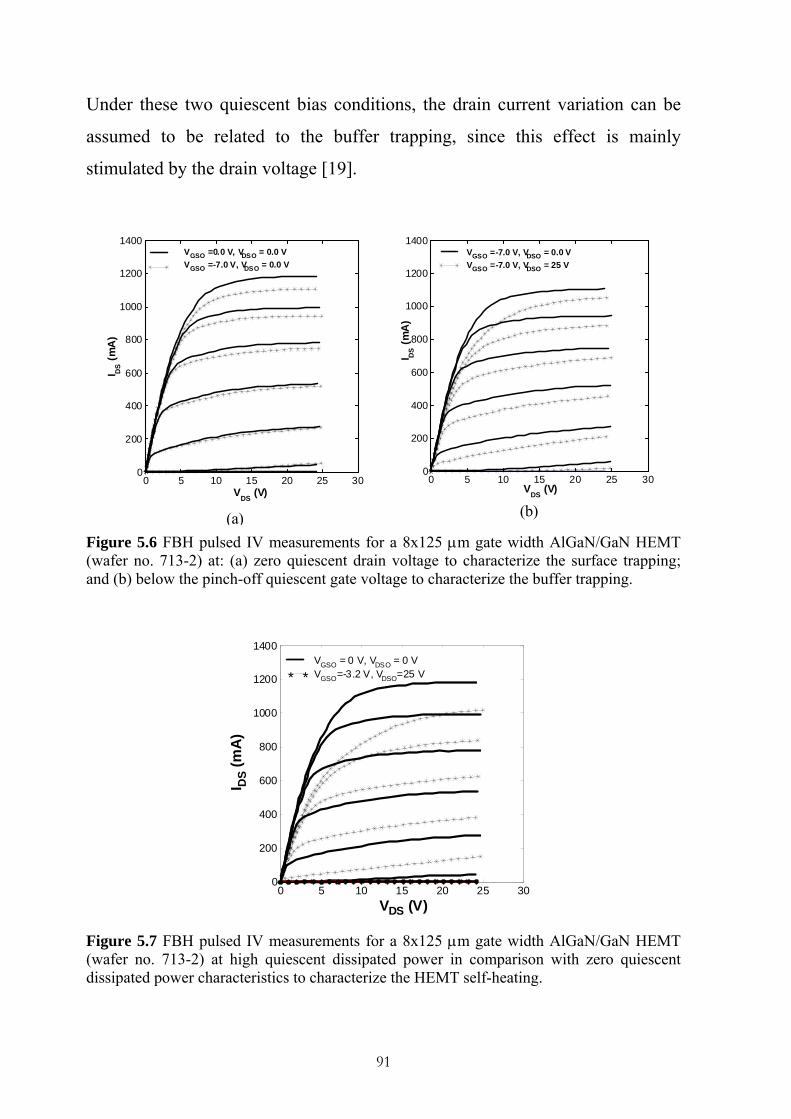
Under these two quiescent bias conditions, the drain current variation can be
assumed to be related to the buffer trapping, since this effect is mainly
stimulated by the drain voltage [19].
0 5 10 15 20 25 300
200
400
600
800
1000
1200
1400
VDS (V)
I DS (m
A)
VGSO =0.0 V, VDSO = 0.0 V VGSO =-7.0 V, VDSO = 0.0 V
(a)
0 5 10 15 20 25 300
200
400
600
800
1000
1200
1400VGSO =-7.0 V, VDSO = 0.0 V VGSO =-7.0 V, VDSO = 25 V
I DS (m
A)
VDS (V) (b)
Figure 5.6 FBH pulsed IV measurements for a 8x125 µm gate width AlGaN/GaN HEMT (wafer no. 713-2) at: (a) zero quiescent drain voltage to characterize the surface trapping; and (b) below the pinch-off quiescent gate voltage to characterize the buffer trapping.
0 5 10 15 20 25 300
200
400
600
800
1000
1200
1400
VDS (V)
I DS
(mA
)
* *VGSO = 0 V, VDSO = 0 VVGSO=-3.2 V, VDSO=25 V
Figure 5.7 FBH pulsed IV measurements for a 8x125 µm gate width AlGaN/GaN HEMT (wafer no. 713-2) at high quiescent dissipated power in comparison with zero quiescent dissipated power characteristics to characterize the HEMT self-heating.
91

To characterize the self-heating, another pulsed IV characteristics at rather high
quiescent power dissipation, shown in Figure 5.7, are used. DC IV
characteristics can also be used in addition to the pulsed IV characteristics for
further improvement of the self-heating characterization.
5.4.3 Drain Current Model Fitting Parameter Extraction
The drain current model equation in (5.3) has four unknowns Ids,isoDC, αG, αD, and
αT. To determine these unknowns, the equation should be applied to at least four
pulsed IV characteristics at suitable quiescent bias conditions that lead to four
independent linear equations. The IV characteristics in Figure 5.6 and Figure 5.7
define approximately four independent states for the drain current. At each state,
the drain current can be assumed to be affected by at most one of the dispersion
sources (surface trapping, buffer trapping, or self-heating). By solving the four
linear equations, corresponding to the four characteristics, at each bias point, the
values of Ids,isoDC, αG, αD, and αT can be determined. Figure 5.8 and Figure 5.9
show the extracted values of these fitting parameters as a function of intrinsic
bias voltages.
05
1015
21
-7-6-5-4-3-2-10 1
0
2
4
6
8
x 10-3
Vds (V) Vgs (V)
αD
05
1015
21
-7-6-5-4-3-2-10
-0.015
-0.01
-0.005
0
Vgs (V) Vds (V)
αG
Figure 5.8 Bias-dependent trapping fitting parameters of the drain current model in (5.3) extracted from the pulsed IV measurements of a 8x125 µm AlGaN/GaN HEMT (wafer no. 713-2).
92

0 5
1015
21
-7-6
-5-4
-3-2
-10
-0.06
-0.04
-0.02
0
Vds (V) Vgs (V) 0 5 10 15 200
0.2
0.4
0.6
0.8
1
1.2
1.4
Vds (V)
I ds,
iso
DC (A
)
Vgs from -7 V to 1 V in step of 0.5 V
(b)
T
α
(a) Figure 5.9 Extracted isothermal DC drain current (a) and bias-dependent self-heating fitting parameter (b) for a 8x125 µm AlGaN/GaN HEMT (wafer no. 713-2).
5.5 Large-Signal Model Implementation
The derived nonlinear elements Qgs, Igs, Qgd, and Igd are written in tables versus
Vgs and Vds in an output file. The fitting bias-dependent parameters , αDCisods,I G,
αD, and αT of the drain current are also written in tables versus Vgs and Vds in
the output file. The intrinsic resistances Rgd and Ri and transconductance time
delay are defined as bias-dependent table-based elements in the same output
file. These elements, which have an orthogonal set of Vgs and Vds can easily be
written in any conventional file format like CITI-file format. Figure 5.10
present the implementation of the table-based large signal model in ADS. The
extrinsic bias-independent elements Cpga, Cpda, Cgda, Lg, Ld, Ls, Cpgi, Cpdi, Cgdi,
Rg, Rd, and Rs are represented by lumped passive elements. The intrinsic
nonlinear part represented by a ten-port Symbolically Defined Device (SDD)
component. The first two ports represent the gate current and charge sources.
The next two ports represent the intrinsic resistances Rgd and Ri. The drain
current is implemented with port no. 5.
93

alpha_Dalpha_GIgdRgd
Ri
IgsQgdQgstau alpha_T
Ids,iso
Gate
Drain
Source
R1Ohm
RRsR=
RRgR=
DataAccessComponentDAC13
iVal2=VdsiVar2="Vds"iVal1=Vgs_tauiVar1="Vgs"InterpDom=RectangularInterpMode=Cubic SplineType=DatasetFile="Ids_713.ds"
DAC
DataAccessComponentDAC11
iVal2=VdsiVar2="Vds"iVal1=Vgs_tauiVar1="Vgs"InterpDom=RectangularInterpMode=Cubic SplineType=DatasetFile="Ids_713.ds"
DAC
DataAccessComponentDAC10
iVal2=VdsiVar2="Vds"iVal1=VgsiVar1="Vgs"InterpDom=RectangularInterpMode=Cubic SplineType=DatasetFile="GaN1mmW713KU.ds"
DAC
DataAccessComponentDAC8
iVal2=VdsiVar2="Vds"iVal1=VgsiVar1="Vgs"InterpDom=RectangularInterpMode=Cubic SplineType=DatasetFile="GaN1mmW713KU.ds"
DAC
DataAccessComponentDAC7
iVal2=VdsiVar2="Vds"iVal1=VgsiVar1="Vgs"InterpDom=RectangularInterpMode=Cubic SplineType=DatasetFile="GaN1mmW713KU.ds"
DAC
DataAccessComponentDAC5
iVal2=VdsiVar2="Vds"iVal1=VgsiVar1="Vgs"InterpDom=RectangularInterpMode=Cubic SplineType=DatasetFile="GaN1mmW713KU.ds"
DAC
DataAccessComponentDAC4
iVal2=VdsiVar2="Vds"iVal1=VgsiVar1="Vgs"InterpDom=RectangularInterpMode=Cubic SplineType=DatasetFile="GaN1mmW713KU.ds"
DAC
DataAccessComponentDAC3
iVal2=VdsiVar2="Vds"iVal1=VgsiVar1="Vgs"InterpDom=RectangularInterpMode=Cubic SplineType=DatasetFile="GaN1mmW713KU.ds"
DAC
DataAccessComponentDAC2
iVal2=VdsiVar2="Vds"iVal1=VgsiVar1="Vgs"InterpDom=RectangularInterpMode=Cubic SplineType=DatasetFile="GaN1mmW713KU.ds"
DAC
DataAccessComponentDAC6
iVal2=VdsiVar2="Vds"iVal1=Vgs_tauiVar1="Vgs"InterpDom=RectangularInterpMode=Cubic SplineType=DatasetFile="Ids_713.ds"
DAC
DataAccessComponentDAC1
iVal2=VdsiVar2="Vds"iVal1=Vgs_tauiVar1="Vgs"InterpDom=RectangularInterpMode=Cubic SplineType=DatasetFile="Ids_713.ds"
DACVARVAR53Vgs_tau=_v10
EqnVar
VARVAR54jw=j*omega
EqnVar
VARVAR13
Vds=_v5Vgs=_v1
EqnVar
SDD10PSDD10P1
H[4]=exp(-1*jw*tau)H[3]=1H[2]=1F[10,4]=_v10-_v1F[9,0]=_i9-_v6F[8,3]=_i8F[7,2]=_i7F[6,0]=_i6-(_i5*_v5)F[5,0]=_i5-IdsF[4,0]=if (Rgd> 0) then Rgd*_i4-_v4 else (0-_v4) endifF[3,0]=if (Ri> 0) then Ri*_i3-_v3 else (0-_v3) endifI[2,1]=QgdI[2,0]=IgdI[1,1]=QgsI[1,0]=Igs
VARVAR56Ids=Ids_iso+alpha_G*_v7+alpha_D*_v8+alpha_T*v9
EqnVar
CCpgaC=
CCGT
RRGT
CCpgiC=
CCgdaC=
RRDT
CCDT
R1ohm
RRdR=
LLd
R=L=
CCth
RRth
CCgdiC=
LLs
R=L=
CCpda
CCpdiC=
LLg
R=L=
PortP2Num=2
PortP3Num=3
PortP1Num=1
Figure 5.10 Large-signal model implementation in ADS (Advances Design System) software.
94

The transconductance time delay is modeled with a delayed gate voltage in port
no. 10. Port no. 7 and port no. 8 are used to represent the AC components of
the gate and drain voltages, (Vgs-Vgso) and (Vds-Vdso). The instantaneous
dissipated power is calculated in port no. 6 and the low pass circuit, connected
to port no. 9, derives its mean value. Through simulation the values of the
nonlinear elements and the drain current fitting parameters are read from the
data files using Data Access Components (DACs) as illustrated in Figure 5.10.
5.6 Simulation and Measurement Results
The developed large-signal model was verified by independent measurements.
The considered devices are 8x125 µm gate width AlGaN/GaN HEMTs on
different wafers. First, the model is checked whether it is consistent with IV and
S-parameter measurements it has been derived from. Secondly, large-signal
single tone and two-tone simulations are compared with the corresponding
measurements.
5.6.1 S-Parameter
S-parameter simulations in comparison with measurements for 8x125 µm gate
width devices on different wafers are shown in Figure 5.11 and Figure 5.12. In
general, the good agreement between simulation and measurement verifies the
consistency of the large-signal model with the small-signal equivalent circuit
model. As described in the last sections, the nonlinear gate elements of the
model, which strongly influence the simulation of S11 and S12, are extracted
from S-parameter measurements. Therefore, the model gives better simulation
for S11 and S12, as shown in the figures, because of using the same
measurement system to extract and validate the model. However, the drain
current in the model, which influences the simulation of S22 and S21, is
95

extracted from pulsed IV measurements. Therefore, different measurement
systems are used to extract and validate the model with respect to S22 and S21.
freq (150.0MHz to 20.00GHz)
S22
S11
-15 -10 -5 0 5 10 15-20 20
freq (150.0MHz to 20.00GHz)
40xS12
S21
Figure 5.11 Comparison of measured (circles) and simulated (lines) S-parameter for a 8x125-µm AlGaN/GaN HEMT on wafer no. 713-2 at VGS = -2.0 V and VDS = 9.0 V.
-10 -5 0 5 10-15 15
freq (500.0MHz to 20.00GHz)
40xS12
S21
freq (500.0MHz to 20.00GHz)
S22
S11
Figure 5.12 Comparison of measured (circles) and simulated (lines) S-parameter for a 8x125-µm AlGaN/GaN HEMT on wafer no. 398-4 at VGS = -3.0 V and VDS = 21.0 V.
Due to the different measurement uncertainties (calibration procedure, probe
tip position, etc.) in these two systems, small discrepancy between simulated
and measured S22 and S21 can be seen in Figure 5.11 and Figure 5.12. The
96
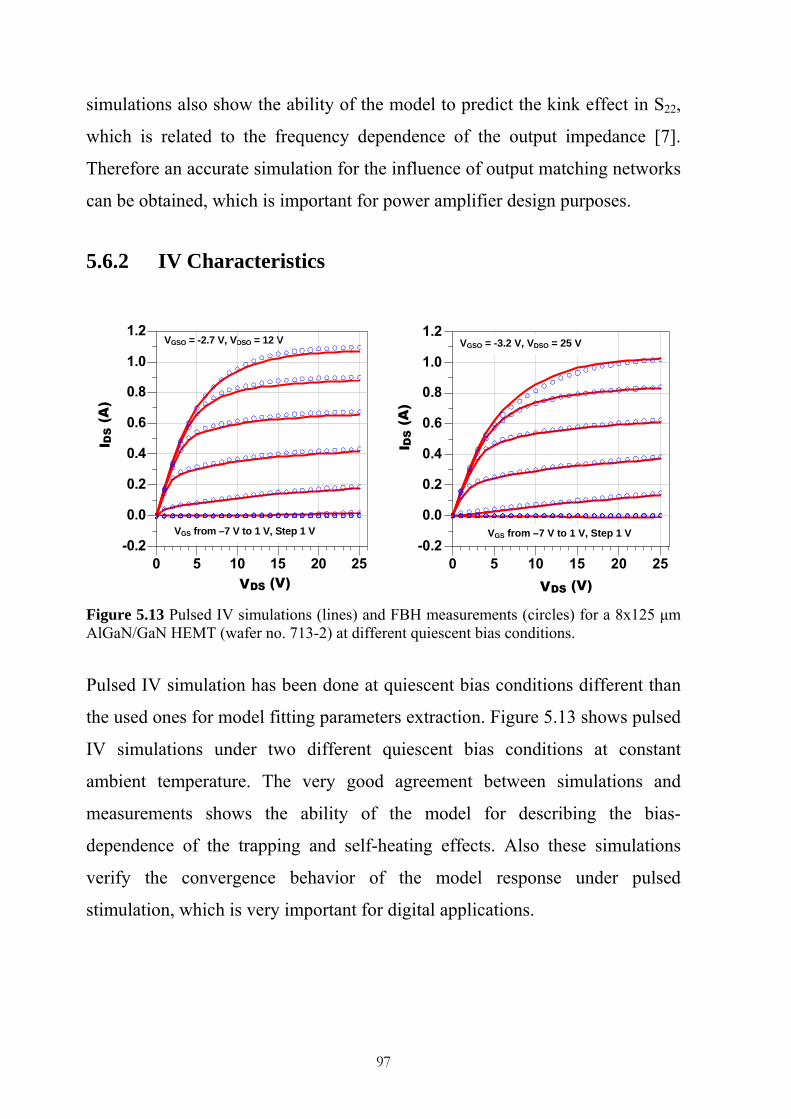
simulations also show the ability of the model to predict the kink effect in S22,
which is related to the frequency dependence of the output impedance [7].
Therefore an accurate simulation for the influence of output matching networks
can be obtained, which is important for power amplifier design purposes.
5.6.2 IV Characteristics
VGSO = -2.7 V, VDSO = 12 V
5 10 15 200 25 5 10 15 200 25
0.0
0.2
0.4
0.6
0.8
1.0
-0.2
1.2
I DS(A)
VDS (V)
VGSO = -3.2 V, VDSO = 25 V
VGS from –7 V to 1 V, Step 1 V 0.0
0.2
0.4
0.6
0.8
1.0
-0.2
1.2
I DS(A)
VDS (V)
VGS from –7 V to 1 V, Step 1 V
Figure 5.13 Pulsed IV simulations (lines) and FBH measurements (circles) for a 8x125 µm AlGaN/GaN HEMT (wafer no. 713-2) at different quiescent bias conditions.
Pulsed IV simulation has been done at quiescent bias conditions different than
the used ones for model fitting parameters extraction. Figure 5.13 shows pulsed
IV simulations under two different quiescent bias conditions at constant
ambient temperature. The very good agreement between simulations and
measurements shows the ability of the model for describing the bias-
dependence of the trapping and self-heating effects. Also these simulations
verify the convergence behavior of the model response under pulsed
stimulation, which is very important for digital applications.
97
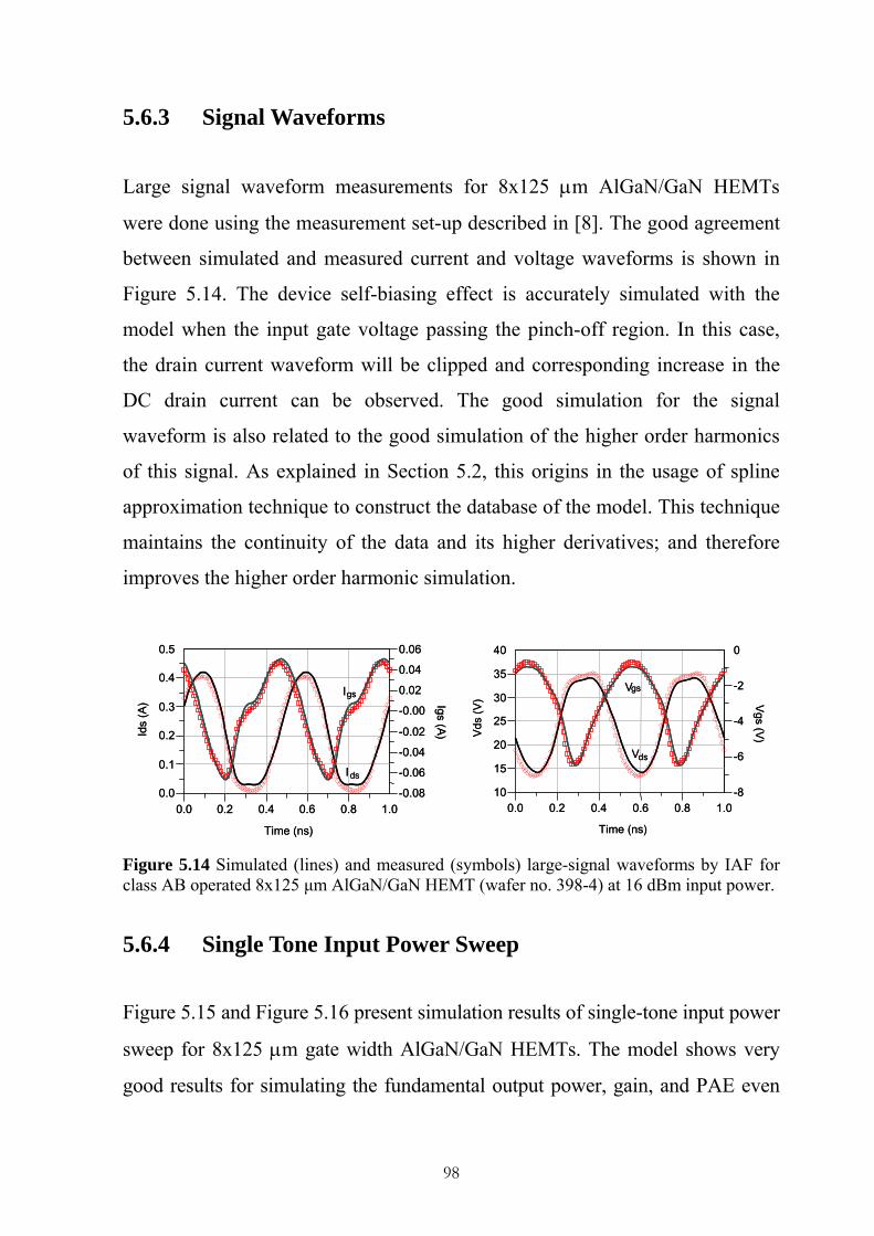
5.6.3 Signal Waveforms
Large signal waveform measurements for 8x125 µm AlGaN/GaN HEMTs
were done using the measurement set-up described in [8]. The good agreement
between simulated and measured current and voltage waveforms is shown in
Figure 5.14. The device self-biasing effect is accurately simulated with the
model when the input gate voltage passing the pinch-off region. In this case,
the drain current waveform will be clipped and corresponding increase in the
DC drain current can be observed. The good simulation for the signal
waveform is also related to the good simulation of the higher order harmonics
of this signal. As explained in Section 5.2, this origins in the usage of spline
approximation technique to construct the database of the model. This technique
maintains the continuity of the data and its higher derivatives; and therefore
improves the higher order harmonic simulation.
0.2 0.4 0.6 0.80.0 1.0
15
20
25
30
35
10
40
-6
-4
-2
-8
0
Time (ns)
Vds
(V) V
gs(V
)
V
V
gs
ds
0.2 0.4 0.6 0.80.0 1.0
15
20
25
30
35
10
40
-6
-4
-2
-8
0
Time (ns)
Vds
(V) V
gs(V
)
V
V
gs
ds
0.2 0.4 0.6 0.80.0 1.0
0.1
0.2
0.3
0.4
0.0
0.5
-0.06
-0.04
-0.02
-0.00
0.02
0.04
-0.08
0.06
Time (ns)
Ids
(A) Igs
(A)
Igs
Ids
0.2 0.4 0.6 0.80.0 1.0
0.1
0.2
0.3
0.4
0.0
0.5
-0.06
-0.04
-0.02
-0.00
0.02
0.04
-0.08
0.06
Time (ns)
Ids
(A) Igs
(A)
Igs
Ids
Figure 5.14 Simulated (lines) and measured (symbols) large-signal waveforms by IAF for class AB operated 8x125 µm AlGaN/GaN HEMT (wafer no. 398-4) at 16 dBm input power.
5.6.4 Single Tone Input Power Sweep
Figure 5.15 and Figure 5.16 present simulation results of single-tone input power
sweep for 8x125 µm gate width AlGaN/GaN HEMTs. The model shows very
good results for simulating the fundamental output power, gain, and PAE even
98

for input power levels beyond the 1-dB gain compression point. The model also
shows good simulation results for the higher harmonic components of output
power up to the third harmonic.
11 13 15 17 199 21 11 13 15 17 199 21
15
20
25
30
10
35
Pin (dBm) P
out-
fund
(dB
m),
Gai
n (d
B)
Gain
Pout
-20
0
20
-40
40
Pin (dBm)
Po
ut
(dB
m)
2fo
3fo
fo
Figure 5.15 Single-tone power sweep simulations (lines) and in-house measurements (symbols) for class A operated 8x125 µm AlGaN/GaN HEMT (wafer no. 713-2) at 2 GHz in a 50 Ω source and load environment.
30
35 40
in (
dB)
Pout
Figure 5.16 Singfor class AB opesource and load e
5.6.5 Two
Tow-tone sim
describes the
conditions. Th
separated by 1
11 13 15 17 199 21
15
20
25
10
10
20
30
0
Pin (dBm)
Pou
t-fu
nd (
dBm
), G
a PA
E (%
)
Gain
PAE
le-tone power sweep simulations (lines) and IAF measurements (symbols) rated 8x125 µm AlGaN/GaN HEMT (wafer no. 398-4) at 2 GHz in a 50 Ω nvironment.
-Tone Input Power Sweep
ulation is typical for device nonlinearity analysis because it
behavior of the device under realistic modulated large-signal
e simulation under a two-tone excitation centered at 2 GHz and
00 kHz was performed. The simulation results are compared
99

with measurements of 8x125 µm gate width AlGaN/GaN HEMTs on different
wafers. These measurements were performed in-house using the developed
measurement set-ups described in [9] and [10]. Figure 5.17 and Figure 5.18
show the simulation results in comparison with the measurements.
5 7 9 11 13 15 173 19 5 7 9 11 13 15 173 19
15
20
25
30
10
35
Pin (dBm)P
out-
fund
(dB
m),
Gai
n (d
B)
Pout
Gain
-10
0
10
-20
20
Pin (dBm)
IMD
3L
(d
Bm
)
Figure 5.17 Simulated (lines) and measured (symbols) output versus input power per tone, under a two-tone excitation centered at 2 GHz and separated by 100 kHz, for class A operated 8x125 µm AlGaN/GaN HEMT (wafer no. 398-4) in a 50 Ω source and load environment.
The model shows very good results for describing the output power and gain
except at high power end. The inaccuracy is due to the extrapolation error
outside the region of measurements where the model was derived from. This
model accuracy can be improved by increasing the range of these
measurements to cover higher voltage conditions.
3 5 7 9 11 13 15 17 191 213 5 7 9 11 13 15 17 191 21
15
20
25
30
10
35
Pin (dBm)
Po
ut-
fun
d (d
Bm
), G
ain
(d
B)
Pout
Gain-25
-15
-5
5
15
-35
25
Pin (dBm)
IMD
3L
(d
Bm
)
Figure 5.18 Simulated (lines) and measured (symbols) output versus input power per tone, under a two-tone excitation centered at 2 GHz and separated by 100 kHz, for class AB operated 8x125 µm AlGaN/GaN HEMT (wafer no. 713-2) in a 50 Ω source and load environment.
100

The model also shows very good simulation for the third order intermodulation
distortion (IMD3). This can also be related to using of the spline approximation
for construction of the model elements data as described in Section 5.2. As can
be noted in Figure 5.17 and Figure 5.18, the model accuracy for describing the
IMD3 is reduced in the low input power range. This can be attributed to the
resolution of the measurements, which are used for the model derivation. The
model accuracy is reduced when the voltages swing is less than the step voltage
of the measured data [11]. This limitation can be overcome by sufficient
density of measurement points especially in the region of strong nonlinearity in
the IV characteristics. Also using spline approximation during the ADS
simulation itself can improve the IMD3 simulation in the low power levels [3].
0 2 4 6 8 10 12 14 16 18-2 20
-30
-20
-10
0
10
-40
20
Pin (dBm)
IMD
3L
(d
Bm
)
Class A (40%I )Class AB (5%I )Class C (V < V )
DSS DSS
GS P
0 2 4 6 8 10 12 14 16 18-2 20
20
30
40
10
50
Pin (dBm)
IMR
(d
B)
Class A (40%I )Class AB (5%I )Class C (V < V )
DSS
DSS
GS P
Figure 5.19 Simulated lower intermodulation distortion and carrier to intermodulation ratio versus input power per tone, under a two-tone excitation centered at 2 GHz and separated by 100 kHz, for a 8x125 µm AlGaN/GaN HEMT (wafer no. 713-2) under 20 V drain bias voltage for different gate bias voltages in a 50 Ω source and load environment.
Figure 5.19 shows simulated lower IMD3 and the corresponding carrier to
intermodulation ratio (IMR) for 8x125 µm gate width AlGaN/GaN HEMT
under two-tone excitation for different classes of operation. The model shows
very good results for prediction of the IMD3 sweet spots (local minima), which
results from the interaction between small- and large signal IMDs [12], [13],
[14]. The IMD3 simulation was done at different gate bias conditions for 20V
drain biased device in a 50 Ω source and load environment. It is found that the
101

best performance with maximum IMR and high power added efficiency could
be obtained when the device is biased just above the pinch-off voltage as
illustrated in Figure 5.19. These results are in a very good agreement with the
reported ones in [15] for a 2-mm gate width AlGaN/GaN HEMT.
References
[1] G. Meneghesso, G. Verzellesi, R. Pierobon, F. Rampazzo, A. Chini, U. K. Mishra, C. Canali, and E. Zanoni, “Surface-related drain current dispersion effects in AlGaN-GaN HEMTs,” IEEE Trans. Microwave Theory & Tech., vol. 51, pp. 1554-1561, October 2004.
[2] E. Kohn, I. Daumiller, M. Kunze, M. Neuburger, M. Seyboth, T. J. Jenkins, J. S. Sewell, J. Van Norstand, Y. Smorchkova, and U. K. Mishra, “Transient characteristics of GaN-based heterostructure field-effect transistors,” IEEE Trans. Microw. Theory Tech., vol. 51, pp. 634-641, February 2003.
[3] V. Cuoco, M.P. van den Heijden, and L.C.N de Vreede, “The “smoothie” data base model for the correct modeling of non-linear distortion in FET devices,” International Microwave Symposium Digest, Seattle, WA, pp. 2149-2152, February 2002.
[4] K. Koh, H.-M. Park, and S. Hong, “A spline large-signal FET model based on bias-dependent pulsed I-V Measurements,” IEEE Trans. Microw. Theory Tech., vol. 50, pp. 2598-2603, November 2002.
[5] I. Schmale and G. Kompa, “A physics-based non-linear FET model including dispersion and high gate-forward currents,” International IEEE Workshop on Experimentally Based FET Device Modelling and Related Nonlinear Circuit Design, University of Kassel, Kassel, Germany, pp. 27.1-27.7, July 1997.
[6] C. Charbonniaud, S. De Meyer, R. Quere, and J. P. Teyssier, “Electrothermal and trapping effects characterization of AlGaN/GaN HEMTs,” 11th GaAs Symposium, Munich 2003.
[7] S.-S. Lu, C. Meng, T.-W. Chen, and H. C. Chen, “The origin of the kink phenomenon of transistor scattering parameter S22,” IEEE Trans. Microwave Theory & Tech., vol. 49, pp. 333-340, February 2001.
[8] F. van Raay and G. Kompa, “Combination of waveform and load-pull measurements,” International IEEE Workshop on Experimentally Based FET Device Modelling & Related Nonlinear Circuit Design, University of Kassel, Kassel, Germany, pp. 10.1-10.11, July 1997.
102
[9] A. Ahmed, E. R. Srinidhi, and G. Kompa, “Efficient PA modeling using neural network and measurement set-up for memory effect characterization in the power device, “ IEEE MTT-S Int. Microwave Symposium, WE1D-5, Long Beach, CA, June 2005.
[10] A. Ahmed, B. Bunz, M. Gamal-El Din, and G. Kompa, “Measurement set-ups for memory effects characterization in GaN HEMT power device,“ Top Amplifier Research Groups in a European Team (TARGET) Tutorial on Device Characterisation, Amsterdam, October 2004.
[11] J. Wood and D. Root, “Agilent-Angelov” III-V FET model,” Technical presentation in device modeling seminar, Japan, October 2005, Agilent Technologies, Santa Rosa, CA, USA.
[12] N. B. Carvalho and J. C. Pedro, “Large-and small-signal IMD behavior of microwave power amplifier,” IEEE Trans. Microwave Theory & Tech., vol. 47, pp. 2364-2374, December 1999.
[13] C. Fager, J. C. Pedro, N. B. Carvalho, and H. Zirath, “Prediction of IMD in LDMOS transistor amplifiers using a new large-signal model,” IEEE Trans. Microwave Theory & Tech., vol. 50, pp. 2834-2842, December 2002.
[14] P. M. Cabral, N. B. Carvalho and J. C. Pedro, “An integrated view of nonlinear distortion phenomena in various power amplifier technologies,” 11th GAAS Symposium, Munich, pp. 69-72, October 2003.
[15] P. M. Cabral, J. C. Pedro, and N. B. Carvalho, “Nonlinear device model of microwave power GaN HEMTs for high power-amplifier design,” IEEE Trans. Microwave Theory Tech., vol. 52, pp. 2585-2592, November 2004.
[16] C. de Boor, A practical guide to splines. New York: Springer-Verlag, 1978.
[17] J. C. Pedro and N. B. Carvalho, Intermodulation Distortion in Microwave and Wireless Circuits. Norwood, MA: Artech House, 2003.
[18] I. Daumiller, D. Theron, C. Gaquiere, A. Vescan, R. Dietrich, A. Wieszt, H. Leier, R. Vetury, U. K. Mishra, I. P. Smorchkova, S. Keller, N. X. Nguyen, C. Nguyen, and E. Kohn, “Current instabilities in GaN-based devices,” IEEE Electron Device Lett., vol. 22, pp. 62-64, February 2001.
[19] S. C. Binari, K. Ikossi, J. A. Roussos, W. Kruppa, D. Park, H. B. Dietrich, D. D. Koleske, A. E. Wickenden, and R. L. Henry, “ Trapping effect and microwave power performance in AlGaN/GaN HEMTs,” IEEE Trans. on Electron Devices, vol. 48, pp. 465-471, March 2001.
103

Chapter 6
Conclusion and Future Work
In this thesis, a large-signal model for AlGaN/GaN HEMT, which predicts
trapping and self-heating induced current dispersion and intermodulation
distortion was developed and demonstrated. The model was derived from a
physics-relevant small-signal equivalent circuit model using bottom-up
modeling technique. The small-signal model topology is constructed to account
for the main physical and electrical characteristics of the large size high power
devices. These include distributed parasitic, gate-forward, and gate-breakdown
effects. An efficient method for reliable extraction of the small-signal model
parameters was developed. In the extrinsic parameter extraction part, first,
high-quality starting values for the extrinsic elements were generated using
cold S-parameter measurements. Then, optimal values were searched through
an optimization process. In the intrinsic parameter extraction part, an efficient
technique was proposed for optimal extraction. The accuracy of the developed
extraction method was demonstrated through simulated and measured S-
parameters over a wide bias range. The reliability of the extraction results was
verified in terms of the reverse modeling of the effective gate length. Different
sizes including 100-µm, 1-mm, 2-mm, and 4-mm gate width devices were
investigated. The proposed small-signal equivalent circuit model shows very
good results for describing the small-signal characteristics of these devices
including the distributed parasitic effects, which increased by increasing the
device size. It is found that the model can describe these effects up to 5 GHz
104

operating frequency for 4-mm gate width device. For higher operating
frequencies the extrinsic part of the equivalent circuit can be extended to
account for further parasitics stimulated by the signal frequency. Also for larger
devices the extrinsic circuit can be modified to account for further parasitics
introduced by the complex structure of the device.
The extracted intrinsic gate capacitances and conductances of the small-
signal model were integrated to find the gate charge and current sources of the
large-signal model assuming that these elements satisfy the integral path-
independence condition. It is found that this assumption is valid for the
investigated devices because those elements did not show significant self-
heating dependency. However, for larger devices it is recommended to use
pulsed S-parameter measurements instead of the conventional ones to reduce
the inherent self-heating through the device characterization. The intrinsic
channel conductances are very sensitive for the self-heating and trapping
effects; therefore the drain current cannot be derived in the same manner as the
gate currents and charges. Therefore, pulsed IV measurements under
appropriate quiescent bias conditions were used to accurately characterize the
drain current and the inherent self-heating and trapping effects. It is found that
using approximation technique instead of interpolation once for construction of
the large-signal model database can improve the model capability for
harmonics and IMD simulations. Since the approximation can maintain the
continuity of the higher order derivatives of the currents and charges also it
reduces the influence of the measurement uncertainty especially near the pinch-
off region. Further improvement for the IMD simulation can be obtained by
using the approximation technique in the ADS simulator instead of the built-in
interpolation once. In our case we used this approximation technique to
construct the model database, which are saved in a data file (look-up table) in
the ADS. Through the model simulation, the values of the model nonlinear
element under stimulating voltages are interpolated from the look-up table. Due
105

the nature of this technique, small discontinuities are introduced in the
interpolated values. These results in a non-accurate simulation for those higher
order derivatives and hence deteriorate the IMD simulation. However, using of
the approximation technique can produce smooth variation for the model
element values with the stimulating voltages; and therefore improves the IMD
simulation. The implemented series RC circuits, in the gate and drain sides of
the model, provide improved simulation of the dynamic behavior of the
trapping process. The elements of the RC circuits are assumed as bias
independent and those values are selected to define the typical measured
trapping time constants for AlGaN/GaN HEMT. However, these time constants
can be estimated for example from low frequency S-parameter measurements.
The bias dependence of the RC elements can also be accounted by changing
the values of these elements to minimize the error between the measured and
simulated S-parameter under different bias conditions. Large-signal simulations
show that the model can accurately describe the performance of the device
under constant temperature corresponding to the ambient temperature of the
measurements, which the model has been derived from.
The model capability for simulation at different ambient temperatures can
be accounted by reformulation the drain current model expression to include
the internal (channel) and the ambient temperatures. In this case the device
thermal resistance should be known in order to split its value from the thermal
fitting parameter. Also at high operating temperatures, thermal factors, which
account for the temperature dependency of the other nonlinear model elements
should be included in the model. These factors can be extracted from pulsed S-
parameter measurements at different ambient temperatures. After these
modifications, the model can also be scaled with the gate width to simulate
larger device sizes, which reduce the requirement of additional high-power
equipments to characterize and model these devices.
106

Publications
[1] A. Jarndal and G. Kompa, “A New Small Signal Model Parameter Extraction Method Applied to GaN Devices,” in IEEE MTT-S International Microwave Symposium Dig., Long Beach, CA, June 2005, pp. 1-4.
[2] A. Jarndal and G. Kompa, “A New Small-Signal Modeling Approach Applied to GaN Devices,” IEEE Trans. Microw. Theory Tech., vol. 53, no. 11, pp. 3440-3448, November 2005.
[3] A. Jarndal and G. Kompa, “An Accurate Small-Signal Model for AlGaN-GaN HEMT Suitable for Scalable Large-Signal Model Construction,” IEEE Microw. Wireless Components Lett., vol. 16, no. 6, pp. 333-335, June 2006.
[4] A. Jarndal, Bernd Bunz and G. Kompa, “Accurate Large-Signal Modeling of AlGaN-GaN HEMT Including Trapping and Self-Heating Induced Dispersion,” in IEEE International Symposium on Power Semiconductor Devices and IC’s, Napoli, Italy, June 2006, pp. 1-4.
107


