151
Endalkachew Shewarega Mengistu Large-Signal Modeling of GaN HEMTs for Linear Power Amplifier Design

Endalkachew Shewarega Mengistu
Large-Signal Modeling of GaN HEMTs for Linear Power Amplifier Design

This work has been accepted by the faculty of electrical engineering / computer science of the University of Kassel as a thesis for acquiring the academic degree of Doktor der Ingenieurwissenschaften (Dr.-Ing.). Supervisor: Prof. Dr.-Ing. G. Kompa Co-Supervisor: Prof. Dr. H. Hillmer Defense day: 25th January 2008 Bibliographic information published by Deutsche Nationalbibliothek The Deutsche Nationalbibliothek lists this publication in the Deutsche Nationalbibliografie; detailed bibliographic data is available in the Internet at http://dnb.d-nb.de. Zugl.: Kassel, Univ., Diss. 2008 ISBN: 978-3-89958-381-6 URN: urn:nbn:de:0002-3816 © 2008, kassel university press GmbH, Kassel www.upress.uni-kassel.de Printed by: Unidruckerei, University of Kassel Printed in Germany

Dedicated to the memory of my father


Acknowledgments
I wish to express my special gratitude to my research advisor Prof. Dr.-Ing. G. Kompa, head of the Department of High Frequency Engineering, Kassel University, for giving me the chance to work in different research projects in the past four years. I am very grateful for his continuous support and encouragement in the course of this work. My thanks also goes to our industry research partners for their cooperation by providing devices and some of the measurement data.
I am very grateful to Prof. Dr. H. Hillmer for his time in accepting the task of second examiner of this dissertation. In addition, I would also like to thank the members of the examination committee Prof. Dr.-Ing. J. Börcsök and Prof. Dr. K.-J. Langenberg for accepting to sit in the commission at a short notice.
I am thankful to all members of the Department of High Frequency Engineering for their support and teamwork spirit. My gratitude goes to Dr.-Ing. B. Bunz, Dipl.-Ing. J. Weide, Mrs. H. Nauditt, Mr. A. Zena Markos, Mr. S. Embar, Mr. B. Wittwer, and all others who I did not mention by name. I want to thank them all for their encouragement and comforting help.
Endalkachew Shewarega Mengistu
Dec. 2007

v
Contents
Chapter 1: Introduction 1
1.1 State-of-the-Art Power HEMTs ……………………………….… 2 1.2 Need for Large-Signal Model ……………………………….… 3
Chapter 2: AlGaN/GaN HEMTs 7
2.1 HEMT Structure and Processing ………………………………..… 10 2.1.1 Substrates ………………………………..… 11 2.1.2 Piezoelectric and Spontaneous Polarizations ………..… 11 2.1.3 Epitaxy and Device Fabrication …………………….….… 12
2.1.3.1 Epitaxy ………………………………..… 13 2.1.3.2 Device Fabrication ……………………………….… 15 2.1.3.3 Technology Related Problems .……………….… 17
2.2 Key Power FET Parameters ………………………………..… 18
Chapter 3: Bias-Dependent Linear AlGaN/GaN HEMTs Model 25
3.1 S-Parameter Measurements ………………………… 26 3.2 Electrical Equivalent Circuit Model ……………………………… 28 3.3 Extraction of Extrinsic Parameters …………………………….… 29
3.3.1 Optimizer Based Data Fitting Techniques ………………… 30 3.3.2 Analytical Method ………………………………… 30
3.4 Standard Equivalent Circuit Model 3.4.1 Extrinsic Parameters ………………………………..… 31 3.4.2 Intrinsic Parameters ……………………………..…… 39
3.5 Modified Procedure for Extraction of Extrinsic Elements ………… 42 3.5.1 Improved Parasitic Network ……………………….…. 44
3.6 Small-Signal Model Verification ……………………….…. 50 3.7 Nonlinear Voltage Referencing ………………………..… 52
Chapter 4: Large-Signal Modeling of Power FETs 53
4.1 Data Bases for Large-Signal Model …………………………… 53

vi
4.2 Large-Signal Models for IMD Prediction …………………………… 55 4.3 Top-Down Modeling …………………………… 60 4.4 Device Characterization …………………………… 66
4.4.1 Pulsed DC Measurement …………………………… 69 4.4.1.1 System Requirements …………………………… 70 4.4.1.2 External Temperature Controller …………………… 71 4.4.1.3 Characterization of Dispersion Effects …………… 72 4.4.1.4 Trapping Effects …………………………… 73 4.4.1.5 Thermal Effects …………………………… 77
4.4.2 Transients …………………………… 78 4.4.3 Characterization of High Power HEMTs …………………… 83
Chapter 5: AlGaN/GaN HEMTs Large-Signal Modeling 85
5.1 Nonlinear Charge Modeling …………………………… 86 5.2 Drain Current Models Based on DC I(V) and S-Parameters …… 88 5.3 Data Bases for Dispersive Large-Signal Models …………………… 89
5.3.1 Drain Current Models Based on Pulsed I(V) Measurements …. 92 5.3.2 Diode Current Models …………………………… 98 5.3.3 Thermal Modeling of AlGaN/GaN HEMT Structures …… 100
5.3.3.1 Thermal Resistance …………………………… 104 5.4 Large-Signal Model Equivalent Circuit …………………………… 107
5.4.1 Model Implementation …………………………… 108 5.4.2 Model Verification …………………………… 110
5.4.2.1 Static and Pulsed I(V) Characteristics ..………...….. 111 5.4.2.2 S-Parameters ……………………..…….… 113 5.4.2.3 Large-Signal Waveforms ……………………… … 113 5.4.2.4 Intermodulation Distortion …………………. 115
Chapter 6: Conclusion and Future Work 119
6.1 Key Research Results …………………………… 119 6.2 Future Characterization and Modeling of Power FETs ……………… 122
A. Pulsed DC System Test ………………………………………….… 125
B. Device Stability in Pulsed I(V) Measurements ..…………………… 129
References 131

vii
List of Symbols BVgd Gate-drain breakdown voltage V Cds Drain-source capacitance F Cgd Gate-drain capacitance F Cgs0, Cgd0 Gate-source and gate-drain capacitance of a ‘cold-
FET’ biased below pinchoff F
Cgs Gate-source capacitance F Cpda Parasitic drain-source pad capacitance F Cpdi Drain-source inter-electrode capacitance F Cpga Parasitic gate-source pad capacitance F Cpgi Gate-source inter-electrode capacitance F Cth Thermal capacitance s·W/K e Electron charge (1.602x10⁻¹⁹C) C E Electric field V/cm EF Fermi level eV EC Bottom edge of conduction band eV fT Current gain cutoff frequency Hz fmax Power gain cutoff frequency Hz fD Function modeling traps associated with deep-level A/V fG Function modeling traps associated with surface state A/V fθ Function modeling thermal effects A/K Gfs, Ggs Differential gate-source diode conductance S Gfd, Ggd Differential gate-drain diode conductance S Gm Channel transconductance S Gds Drain-to-source conductance S iGS, iDS Pulsed DC gate-source and drain-source current A IGS, IDS Static DC gate-source and drain-source current A Imax Maximum drain-source current (gate-forward bias) A Idss Saturated drain-source current (zero gate bias voltage) A
ISODSi Isothermal drain source DC current A ISODSI Static DC drain-source current A
LG Gate length µm LDS Drain-source spacing µm LGS Gate-source spacing µm LGD Gate-drain spacing µm Lg , Ld , Ls Gate, drain, and source inductance Η nS Sheet charge concentration (σ/e) cm-2 Pout Output power at Fundamental frequency W Pin RF input power W PDC DC input power W PAE Power Added Efficiency, % Pdiss Instantaneous dissipated power W

viii
Pdiss0, P0 Average dissipated power W PSP Spontaneous polarization induced charge density C/cm2 PPE Piezoelectric polarization induced charge density C/cm2 Qgs Gate-source charge C Qgd Gate-drain charge C Rth Thermal resistance K/W Rg, Rd, Rs Gate, drain, and source resistance Ω Ri Gate-source charging resistance Ω Rc Channel resistance Ω Rgd Gate-drain charging resistance Ω s Gate-pitch (gate-to-gate spacing) µm Sij Scattering parameters T0 Ambient temperature K Tc Chuck (back-plate) temperature K Tch Channel temperature K
echT Estimated channel temperature K
vs Saturation velocity cm/s vGS, vDS Pulsed DC gate-source and drain-source voltage V VGS0, VDS0 Bias gate-source and drain-source voltage V VGS, VDS Terminal gate-source and drain-source voltage V Vgs, Vds Intrinsic gate-source and drain-source voltage V VP Pinchoff gate-source voltage V WG Gate width µm Yij Small-signal admittance parameters S Zg, Zd, Zs Intrinsic gate, drain, and source branch impedance Ω Zij Small-signal impedance parameters Ω
chT∆ Change in channel temperature K e
chT∆ Change in channel temperature, estimated K
εr Relative dielectric permittivity ηd Drain Efficiency % κ Thermal conductivity W/cm·K µ Electron mobility cm2/V·s σ Sheet charge density C/cm2 τ Transit delay time s φB Barrier height V

ix
List of Abbreviations and Acronyms 2-DEG Two-Dimensional Electron Gas 3G Third Generation ACPR Adjacent Channel Power Ratio ADC Analog-to-Digital Converter ADS® Advanced Design System BTS Base Transceiver Station CAD Computer Aided Design CCDF Complementary Cumulative Distribution Function CW Continuous Wave DAC Data Access Component DC Direct Current DiVA Dynamic I(V) Analyzer DPD Digital Predistortion EEC Electrical Equivalent Circuit EER Envelope Elimination and Restoration EVM Error Vector Magnitude FET Field Effect Transistor HPA High Power Amplifier HEMT High Electron Mobility Transistor HFET Heterojunction FET HBT Heterojunction Bipolar Transistor IMD Intermodulation Distortion LDMOS Laterally Diffused MOS LUT Look-up Table MBE Molecular Beam Epitaxy MESFET MEtal-Semiconductor FET MOCVD Metal-Organic Chemical Vapor Deposition MOS Metal-Oxide-Semiconductor MSG Maximum Stable Gain PAE Power Added Efficiency PAR Peak-to-Average Ratio RF Radio Frequency SDD Symbolically Defined Device SFP Source Filed Plate TEC Thermal Expansion Coefficient UMTS Universal Mobile Telecommunications System VNA Vector Signal Analyzer W-CDMA Wideband Code Division Multiple Access WiMAX Worldwide Interoperability for Microwave Access
(Based on IEEE 802.16 Standard) WirelessMAN Wireless Metropolitan Area Network
(Official Name for IEEE 802.16)

xi
Abstract
The availability of high power transistors with superior device qualities and their accurate large-signal models are the prerequisites for a highly linear and efficient power amplifier design process. In particular, the spectral efficient modulation techniques used in mobile communication systems result in signals having a high peak-to-average power ratio. This in turn requires that the power amplifiers be operated at large back-off power levels to avoid spectral spreading. Therefore, spectral efficiency comes at the expense of power efficiency. Consequently, a thorough analysis of the linearity of the power amplifiers is required using computer-aided design (CAD) techniques. This is a convenient and cost effective procedure to meet the stringent linearity requirements of the communication system but at the same time operating the amplifiers at their highest possible efficiency.
The recent advances in developing new power transistors using wide bandgap materials demonstrated high output power, power density, efficiency, and linearity at high frequencies. These new devices include SiC MESFETs and AlGaN/GaN HEMTs.
In this thesis, the large-signal modeling procedure for high power AlGaN/GaN HEMTs is described. The developed electrothermal large-signal model accounts for both trap and thermal related dispersion effects. The research work covers large-signal modeling process, from device characterization through model implementation. Detailed procedures for the extrinsic parameters extraction, pulsed I(V) characterization, transient measurements, dispersive drain current modeling procedure, and table-based large-signal model implementation are described.
As the drain-source current represents the major nonlinearity of a FET, emphasis was given for its accurate characterization and modeling. The main task in this respect is the modeling technique that takes into account the drain current collapse due to traps and thermal effects.
Many other important issues in large-signal modeling process such as thermal modeling and gate forward diode models are also treated. The thermal modeling of the power transistor includes the determination of the thermal resistance and the thermal time constant of the device structure.

xii
The importance of data processing of the nonlinear model parameters of the large-signal model before its implementation in a nonlinear circuit simulator is highlighted. This is essential in avoiding unphysical extrapolation and model convergence problems of the table-based model.
The validity of the developed dispersive large-signal models is tested through large-signal model verification procedures. It is shown that the nonlinear parameters of the device can be simulated reliably even for drive levels well into compression. More importantly, these tests include the intermodulation distortion prediction capability of the large-signal model, which showed good match to measurement results.

xiii
Zusammenfassung
Die Verfügbarkeit von Hochleistungstransistoren mit ausgezeichneten Bauelement-Eigenschaften und entsprechenden zuverlässigen Großsignalmodellen sind die Grundvoraussetzungen für den Entwurf hocheffizienter und hochlinearer Leistungsverstärker. Besonders die Modulationsverfahren moderner mobiler Kommunikationssysteme führen zu hohem Peak-to-Average Power Ratio. Daher werden Leistungsverstärker bei großem Backoff betrieben, um ein Übersprechen des Nutzsignals in Nachbarkanäle zu vermeiden. Damit erreicht man eine spektrale Effizienz auf Kosten der Leistungseffizienz. Einer genauen Analyse des Linearitätsverhaltens von Leistungsverstärkern mit Hilfe von CAD (Computer Aided Design) Programmen kommt daher große Bedeutung zu. CAD bietet ein geeignetes und kostengünstiges Verfahren, um den strengen Linearitätsanforderungen von Kommunikationssystemen zu genügen und gleichzeitig den Verstärker mit höchstmöglichem Wirkungsgrad zu betreiben.
Neue Leistungstransistoren, bei deren Entwicklung Materialien mit großen Bandlücken verwendet wurden, zeichnen sich durch hohe Ausgangsleistungen, Effizienz und Linearität bei hohen Frequenzen aus. Zu den genannten Transistoren zählen SiC MESFETs und AlGaN/GaN HEMTs.
In dieser Arbeit wird eine Verfahren zur Großsignalmodellierung von AlGaN/GaN Power-HEMTs beschrieben. Das entwickelte elektro-thermische Großsignalmodell berücksichtigt Dispersionseffekte, welche sowohl durch Störstellen als auch durch Temperatureffekte verursacht werden. Die Forschungsarbeit umfasst den gesamten Großsignal- Modellierungsprozess, angefangen von der Charakterisierung bis zur Modell-Implementierung. Detaillierte Prozesse zur extrinsischen Parameterextraktion, gepulsten I(V) Charakterisierung, transienten Messung und Modellierung dispersiver Drainströme, sowie die Implementierung tabellenbasierter Großsignalmodelle werden beschrieben.
Da der Drain-Source-Strom die Hauptquelle von Nichtlinearitäten eines FETs ist, wurde dessen genauer Charakterisierung und Modellierung besondere Aufmerksamkeit geschenkt. Das Hauptaugenmerk lag dabei auf der Entwicklung einer geeigneten Modellierungstechnik, die die starke Abnahme des Drainstroms berücksichtigt, welche durch Trapping- und Temperatureffekte hervorgerufen wird.

xiv
Weitere wichtige Punkte des Großsignal-Modellierungsprozesses, wie das thermische Modell und das Gateforward-Modell, werden ebenfalls behandelt. Die thermische Modellierung von Leistungstransistoren beinhaltet die Bestimmung des thermischen Widerstandes sowie die Bestimmung der thermischen Zeitkonstante der Transistorstruktur.
Besonders hervorzuheben ist die sorgfältige Aufarbeitung der gewonnenen Daten des Großsignalmodells, bevor es in einem Programm zur Simulation nichtlinearer Schaltungen verwendet werden kann. Dadurch können unphysikalische Daten aufgrund von Extrapolations- und Konvergenzproblemen bei einem tabellenbasierten Modell verhindert werden.
Die Gültigkeit der entwickelten dispersiven Großsignalmodelle wird mit Hilfe entsprechender Großsignal-Verifikationsprozeduren überprüft. Die Ergebnisse zeigen, dass die nichtlinearen Ausgangparameter wie die Ausgangleistung des Transistors bis weit in die Kompression simuliert werden können. Wichtiger ist jedoch, dass das entwickelte Modell auch Intermodulationsprodukte zuverlässig vorhersagt, was durch gute Übereinstimmung zwischen Messung und Simulation nachgewiesen wurde.

1
Chapter 1
Introduction
Power amplifiers at RF and microwave frequencies find variety of applications including cellular handsets, cellular infrastructure, WLAN, wireless broadband (such as WiMAX), satellite, military, and avionics. Particularly, the rapid growth of wireless communication necessitated power amplifiers in 1 GHz and 2 GHz range for mobile handsets and base transceiver stations (BTS). The market of handset units and BTS is over half billion and in hundreds of thousands units per year respectively [1].
High power amplifiers (HPA) are main components of wireless base transceiver stations. The HPAs for such wideband basestation applications must meet stringent specifications. These specifications are aimed mainly to control signal interference between adjacent communication channels. The HPAs must enable the BTS to comply with the linearity requirements and at the same time operate at the highest possible efficiency.
In general, the required performance qualities of the HPAs are high output power, linearity, gain, efficiency, size and cost. Linearity and efficiency are diametrically contrasting requirements and HPA design strategy is to improve one without compromising the other. The key component of the HPA is, of course, the power transistor(s) used. For example, power-combining schemes must be reduced or avoided by using high power devices to minimize system efficiency degradation. Hence, the availability of power transistors with high output power and other excellent qualities (linearity, gain, efficiency, large input and output impedances) is a prerequisite for designing efficient and linear HPAs.

2
1.1 State-of-the-Art Power FETs
The technologies currently in use for HPA design such as Si-LDMOS are reaching their limits [2]. The main constraint being their operating frequency range which is limited to about 4 GHz. Therefore, intensive research in recent years has made it possible to develop new device process technologies using new wide bandgap materials. The most promising of these is AlGaN/GaN high electron mobility transistors (HEMTs) with record power densities up to 30 W/mm on SiC substrates [3], 9.4 W/mm on GaN substrates [4], 12 W/mm on silicon substrates [5] and 12W/mm on sapphire substrates [6]. However, these reported works are usually for small-size devices and typical power densities are 2 to 5 W/mm for larger devices. Nevertheless, these works indicate an improvement by factor of 10 or more in power densities as compared to other material technologies based on GaAs or silicon.
The input and output impedances of new semiconductor devices is also large due to their high power densities. These and other good qualities translate in simplifying the design of HPAs for applications such as basestations in mobile communication system.
However, the technology of processing AlGaN/GaN HEMTs is not still mature and some technological issues such as drain current collapse, reliability and appropriate packaging for thermal management remain to be solved consistently. Current collapse is the reduction of the drain current (also called DC-RF dispersion or knee walkout or current slump) due to trapping effects. This effect is observed when the device operates under RF excitation. Therefore, devices with substantial current collapse will have reduced RF output power due to the reduced RF current and voltage swings. Since the power density per chip is high for these new devices, good thermal management in conjunction with appropriate packaging technologies is also very important.
Many researchers are already reporting complete high efficiency HPAs based on AlGaN/GaN HEMTs. As an example, HPAs using AlGaN/GaN HEMTs on SiC and Si substrates may be cited here. A power amplifier designed using two 48 mm AlGaN/GaN HEMTs on semi-insulating SiC substrates and producing a saturated output power of 370W (drain bias of 45V) with linear gain 11.2 dB at 2.14 GHz under W-CDMA input signal was published in [7]. The ACLR for this HPA is -36 dBc at 5 MHz offset

3
and the drain efficiency is 24% at 8 dB back-off from saturation output power.
Another group reported a power amplifier having 110W output power (at drain bias of 60V) with linear gain of 13 dB at 2.14 GHz using AlGaN/GaN HEMTs on semi-insulating SiC substrates [8]. Moreover, it is shown that the amplifier linearity has been improved using a digital predistortion system demonstrating a drain efficiency of 24% with ACLR of less than –50 dBc at 42 dBm output power level for a 4-carrier W-CDMA input signal.
Regarding AlGaN/GaN HEMTs on Si substrates, a single 36 mm HEMT chip, producing pulsed RF output power of 368W (at drain bias of 60V), maximum drain efficiency of 70% and 17.5 dB small signal gain has been published [9]. And for a 2-carrier W-CDMA signal, the reported output power is 20.5W (drain bias of 48V) at 8 dB back-off with 35% drain efficiency.
These superior efficiency and linearity figures indicate how the AlGaN/GaN HEMTs have profoundly changed the outcome of microwave HPAs design. Microwave HPAs with efficiencies of about 30% or better have been attained for high linearity applications.
It is necessary to note that these results are attributed to the progress in solving the problem of drain current collapse due to trapping effects. As improvements in AlGaN/GaN HEMT processing technology are still in progress, even better results are expected in future. Another important implication of current collapse free device is the possibility to use a standard digital predistortion (DPD) system to successfully linearize an HPA based on these devices [10]. In both SiC and Si substrates based AlGaN/GaN HEMTs, considerable linearity improvements are obtained using DPD technique. Hence, enabling the PA to fulfill cost effectively, the wideband basestation linearity requirements.
1.2 Need for Large-Signal Model
There are two approaches in the design and optimization of a HPA. These are based either on load-pull measurements [11] and/or on large signal nonlinear device model simulations. Obviously, the second approach requires an accurate large signal model of the device(s) and is the preferred method owing to its convenience and cost effectiveness.
4
The importance of an accurate electrothermal FET model for CAD, in the course of designing a highly linear power amplifier, may be highlighted as follows. Digital modulation schemes and air interfaces in mobile communication systems demand highly linear high power amplifiers (HPAs). The reason being that these spectrum efficient modulation techniques result in a non-constant envelope signal. This in turn requires the HPA be operated at large back-off (i.e. at low efficiency) to avoid spectral spreading. Hence, the increase in bandwidth efficiency comes at the expense of power efficiency. This is very costly to the communication system operator. It is, therefore, necessary to have a linear HPA in order to increase the power efficiency of the system in general and that of the power amplifier in particular. Consequently, the design of a linear HPA may require:
1. Application of linearization techniques, such as digital predistortion (DPD), to the designed quasi-memoryless HPA. Linearization is required in order to operate the HPA at higher output power levels (improved efficiency) but still satisfying linearity requirements. A meaningful linearity improvement using a DPD implementation necessitates a quasi-memoryless HPA.
2. Methods to reduce memory effects (e.g. gate- and drain-bias circuits with low baseband impedances) resulting in a quasi-memoryless HPA. Memory effects may be defined as the dependence of intermodulation distortion (IMD) on baseband and RF frequency. Since the baseband impedance variation with envelope frequency is much more significant than that of the RF impedance, it is the major contributor to memory effects [12].
3. The implementation of complex HPA architectures such as envelope elimination and restoration (EER) and Doherty to enhance efficiency.
In order to carry out such tasks at computer simulation levels, the availability of an accurate nonlinear large-signal model of the power transistor(s) is a key criterion. These complex tasks require a large-signal model developed based on reliable measurement data, correct modeling technique and proper model implementation. These steps ensure optimum design approach for a short design-to-production cycle.
Even though, several types of large signal nonlinear models are reported in literature, only few of them report on linearity prediction

5
capabilities of their models. This is particularly true for large-signal models developed for high power AlGaN/GaN HEMTs. Several issues must be addressed regarding large-signal modeling in general and lookup table-based models in particular. Among these are model consistency, dispersion effects, model implementation in nonlinear simulator (e.g. interpolation and extrapolation problems) and continuous differentiability of the nonlinear model parameters. This thesis was targeted to addressing some of these issues.
The research work presented in this thesis is, therefore, sectioned as follows. Chapter 1 describes the problems to be addressed and the motivation behind such a demanding task. The state of art of the new AlGaN/GaN HEMTs is briefly reviewed and the associated problems due to technology immaturity are summarized. Specially, the need for large-signal model that can able to simulate intermodulation distortion has been emphasized.
Chapter 2 gives an overview of the technology of AlGaN/GaN HEMTs including material properties, suitable substrates, and device structure and processing. Key figure of merits of power HEMTs are also summarized.
The multi-bias small-signal modeling of power AlGaN/GaN HEMTs is detailed in Chapter 3. The extraction of the linear parasitic and the bias dependent nonlinear intrinsic elements of a distributed small-signal equivalent circuit model are discussed.
The large-signal modeling of FETs is covered in Chapter 4 and 5. The first part in Chapter 4 discusses a simplified analysis of the generation of IMDs and the requirements of the large-signal model for their accurate prediction. This is then followed by a brief summary of an earlier research work (Top-down modeling approach) that attempted to address model consistency problem and dispersion effects. The second part treats pulsed I(V) measurements for characterization of power FETs. These characterizations include transient drain current measurements for obtaining time constants related to thermal and trapping effects. The measurement results and other derived parameters for AlGaN/GaN HEMTs are inputs for a dispersive nonlinear drain current model. The determination of dispersive drain current model is the main outcome in Chapter 5. Other issues include the thermal modeling of AlGaN/GaN HEMT structures and the derivation of the gate current model from pulsed I(V) measurements. Finally, the lookup table based large signal model implementation and

6
verification are presented. Conclusions and required improvements in future works are discussed in Chapter 6.

7
Chapter 2
AlGaN/GaN HEMTs
The need for highly linear, efficient and high output power amplifiers (HPAs) for current and future modulation schemes and air interfaces has been emphasized in the last chapter. A typical set of requirements of RF power transistors for 3rd generation mobile communication power amplifiers market is shown in Table 2.1 below [13]. Since the linearity of a device is tested at a large back-off power using W-CDMA signal, the 10W to 40W average output powers correspond to peak output powers of about 70W and 280W, respectively. A typical linearity test measurement standard is a two carrier WCDMA signal having a peak-to-average power ratio of 8.5 dB at 0.01% probability on CCDF (Test Model 1 with 64 users) [9]. Obviously, the efficiency of the devices at such average power levels is much lower than the efficiency at peak power. However, many newly available AlGaN/GaN HEMTs have already specifications with device performance metrics (power, linearity, efficiency, gain etc.) better than the requirements listed in Table 2.1.
Table 2.1: Typical requirements of HPAs for 3G applications (after [13])
RF Power Transistors Property W-CDMA output power (W) 10 to 40 ACPR linearity (dBc) -45 to –39 Drain efficiency at linear operation (%) 22 to 30 Gain (dB) 12 to 15

8
For high power, high frequency applications such as basestation power amplifiers, silicon LDMOS is dominating the market at present [14]. Other devices (e.g. GaAs HEMTs and HBTs, SiGe HBTs) are for relatively low power and/or high frequency applications.
However, the power density of Si-LDMOS is 5x to 10x lower than GaN HEMT [15]. Moreover, AlGaN/GaN HEMTs have reached the commercialization phase and are becoming available from a number of companies. These new devices make the design of HPAs more efficient (e.g. reduction in number of power combining circuits), compact, easier and reliable. The main reason being that for the same output power, AlGaN/GAN HEMTs are smaller than conventional devices. The high power density of these new devices enables to reduce the total gate width required or the number of units cells connected in parallel. The reduced sizes also imply that the devices have higher input and output impedances (e.g. see section 9.2.2 in [16]), which makes matching network design easier.
The key desirable semiconductor material properties for high power and high frequency transistors include large bandgap, high breakdown voltage, high electron velocity and mobility, high sheet charge density (in HEMTs) and high thermal conductivity. Table 2.2 lists these material properties for GaN and other competing materials. The listed electron mobility under the column GaAs and GaN are for AlGaAs/InGaAs and AlGaN/GaN heterostructures.
Table 2.2: GaN and other competing material properties (adopted from [17] - [19])
Attribute Si GaAs 4H-SiC GaN Bandgap (eV) 1.11 1.43 3.2§ 3.4§ Critical electric field (106 V/cm) 0.7 0.7 3.5§ 3.5§ Electron mobility (cm2/V-s) 1500 8500* 700 1000-
2000* Hole mobility (cm2/V-s) 450 330 120 300 Saturation (peak) electron velocity (107 cm/s) 1.0 (1.0) 1.3 (2.1)‡ 2.0 (2.0) 1.5 (2.1) ‡
Thermal conductivity (W/cm·K) 1.5 0.46 4.9 1.5 Relative dielectric constant 11.9 12.5 10 9.5
Significance of Attributes: § High Voltage, ‡ High Frequency * Typical 2-DEG mobility for AlGaAs/InGaAs and AlGaN/GaN heterostructure.
The significance of these material parameters for the power and speed of device capabilities can be summarized as follows. The wide energy

9
bandgap and high critical electric field enable high terminal voltage operation of the transistor. This is essential for high RF power generation. The electron transport properties (electron mobility and saturation velocity) determine its high frequency characteristics. The high sheet charge density of two-dimensional electron gas (2-DEG) in AlGaN/GaN HEMT is one of its peculiar useful properties for maintaining high current densities. Good thermal conductivity is very essential for power transistors to avoid performance degradation with increased channel temperature. Moreover, these new devices can operate at much higher ambient temperature than silicon transistors. Experiments showed that a GaN transistor is amplifying well at ambient temperature of 300°C while silicon transistors stop working at about 140°C [19]. The relatively lower dielectric constant of wide bandgap semiconductors permits a solid-state device to be larger in area for specified impedance level [18]. This in turn helps larger RF currents and higher RF power to be generated. The low dielectric constant also means low capacitive loading of a device [18]. This reduces the parasitic delay contributions to the total delay time (e.g. see section 8.3 in [17]) in the HEMT. The charging time for the parasitic pad, for example, is lower with reduced pad capacitance (Cpad ∝ εr). These and other relationships between material properties, device figures of merit and system level advantages are summarized in Table 2.3.
Table 2.3: Device and system level performance advantages of using wide bandgap materials for power transistors (adopted from [17])
Material Property Device Operates Improved Device Figures of Merit
System Advantage
- High breakdown field
• High voltage operation
• High doping
• Power density • Power gain • Efficiency • Output impedance • IMD
• Increased BW • Smaller number
of die per system• Efficiency
- High thermal conductivity
- Wide bandgap
• High temperature
• Smaller die size • More power/die
• Smaller and cheaper package
- High electron velocity
• High frequency
• High fT and fmax • High system frequency
In general, the main disadvantage of wide bandgap semiconductors is
their low charge carrier mobility [17]. However, the mobility of both 4H-SiC and 2-DEG AlGaN/GaN heterostructures are adequate for fabrication of high performance transistors [18].
10
SiC MESFETs are also suited for high temperature and high voltage operation due to their natural properties. The fabrication technology of SiC MESFETs is more mature than GaN HEMTs but they lack heterojunction and hence the low electron mobility (despite their high saturation velocity) places limitation for high frequency application. Of the many known SiC crystal prototypes, the 3C, 4H and 6H prototypes are useful for electronic design applications. Particularly, the electron mobility of 4H-SiC is about twice that of 6H-SiC and hence preferred for device applications. The designations “C” and “H” refer to cubic and hexagonal crystal structure while the numbers 3, 4 and 6 refer to the Si and C atoms arrangement [18].
2.1 HEMT Structure and Processing
Detailed description of the device processing technology is beyond the scope of this thesis but brief literature review of vital characteristics of AlGaN/GaN HEMTs is presented in the following sub-sections.
Since the invention of high electron mobility transistors, HEMTs (also known as modulation-doped field effect transistor, MODEFT or heterostructure field effect transistor, HFET) in 1980, the processing technology has progressed significantly. Particularly, the processing technology of AlGaN/GaN HEMT has advanced greatly since the mid 1990s thus a record 30W/mm power density was reported [3].
The basic concept in a HEMT is the aligning of a wide and narrow bandgap semiconductor adjacent to each other to form a heterojunction. Specifically, in AlGaN/GaN HEMTs, the carriers from a doped wide energy gap material (AlGaN) diffuse to the narrow bandgap material (GaN) where a dense 2-DEG is formed in the GaN side but close to the boundary with the AlGaN. The Fermi energy of this thin layer is above the conduction band thereby making the channel highly conductive. The ratio of aluminum to gallium in AlGaN is typically 30% Al and 70% Ga. The resulting compound, AlxGa1-xN, has a higher energy bandgap and different material properties from GaN.
The major obstacle in fabrication of GaN HEMTs is the lack of a suitable substrate, which is lattice-matched and thermally compatible material with GaN. Bulk GaN substrates are not commercially available and hence silicon carbide (SiC), sapphire (Al2O3) or silicon (Si) substrates are used instead.

11
2.1.1 Substrates
The choice of suitable substrate is a key issue for companies competing in commercialization of GaN HEMTs. The advantages of Si substrate as compared to SiC or sapphire include wafer cost (≈ 10% of sapphire or ≈ 1% of SiC), availability in larger wafer size and better thermal conductivity than sapphire. The disadvantages include its low resistivity and its large lattice and thermal expansion mismatch to GaN. The lattice mismatch between GaN and the three commonly used substrates (see Table 2.4) can be calculated as substratesubstratelayer /a)a(aa −=∆ where substratea is the lattice constant of the substrate in the epitaxial plane [20].
SiC is the substrate of choice for high power applications due to its good thermal properties, which is nearly 10 times that of sapphire. The reduced lattice mismatch between SiC substrate and GaN or AlN improves the epitaxial quality and reduces dislocations densities [20]. But SiC substrate is expensive. Very recently, Cree Inc. demonstrated the so-called “zero-micropipe” SiC substrates. These defect free substrates, available in 100 mm (4 inch) diameter, are likely to improve yield and eventually lower manufacturing costs.
The other contender, sapphire, is relatively inexpensive but it has poor thermal conductivity. However, other thermal management techniques such as flip-chip mounting technology have been used to make AlGaN/GaN HEMTs on sapphire competitive. GaN HEMTs have also been produced using freestanding GaN substrates [4].
Table 2.4: Physical properties of substrates (adopted from [21]) Attribute Si(111) Sapphire
(c-plane) 4H-SiC
Thermal conductivity (W/cm·K) 1.5 0.42 4.9 Lattice mismatch with GaN (%) ∼ -17 ∼ -16 ∼ +3.5 Currently available wafer size (inch) 12 6 4 Cost (compared to Si) Low Low High Resistivity (Ω cm) Max 104 > 106 105 – 108
2.1.2 Piezoelectric and Spontaneous Polarizations
The origin of 2-DEG in AlxGaxN/GaN HEMT is from a combined spontaneous PSP and piezoelectric PPE polarization effects [22]. Many researchers reported that appreciable 2-DEG is formed at the AlGaN/GaN

12
interface even if all the layers are grown without intentional doping. The 2-DEG sheet carrier density is a function of a number of physical properties such as AlGaN/GaN crystalline face (N- or Ga-face), alloy composition, and thickness of the AlGaN layer [22]. It was observed that the sheet carrier density of the 2-DEG increases with aluminum content of the AlGaN layer for both N- and Ga-face pseudomorphic grown heterostructures [22]. The Ga-face interfaces are uniform and flat and hence result in a better heterostructure structural quality [23].
Now considering Ga-face heterostructures only, the spontaneous polarization PSP for GaN and AlN are negative (i.e. pointing towards the substrate). The piezoelectric polarization along the [0001] axis is positive for compressive and negative for tensile strained barriers, respectively. Since there is a 2.4% lattice mismatch between unstrained AlN and GaN at room temperature, the tensile stress caused by the growth of AlxGaxNx layer on GaN results in a piezoelectric polarization. This piezoelectric polarization, in the strained AlGaN layer, is in parallel with the net spontaneous polarization. Therefore, the total polarization in the AlGaN layer is the sum of the spontaneous and piezoelectric polarizations [22]. Consequently, the polarization induced sheet charge density (σ), which is proportional to the change in polarization across the interface, is large in AlGaN/GaN based transistor structures.
The high sheet charge concentration (nS = σ/e) of ~ 1 - 2x1013 cm-2, which is 3 to 10 times the sheet charge concentration usually achieved in GaAs based HEMTs, enables AlGaN/GaN HEMTs to maintain much higher current densities ( sSdss vneI ∝ ) than other III-V HEMTs. AlGaN/GaN HEMTs with peak currents of 1 A/mm or more at zero gate bias are quite common. Additionally, the high sheet charge density also makes possible very low turn-on resistance, as the channel resistance at low electric field is proportional to ( )Ene/ S µ1 . This in turn improves the high frequency performance of the device (fT and fmax).
2.1.3 Epitaxy and Device Fabrication
The composition of layered structure and the thickness of an AlGaN/GaN HEMT vary with the type of substrates used. These are the nucleation layer, buffer, spacer, carrier supply, barrier, and cap layers. The basic structure shown Fig. 2.1 is used to describe the fundamental operational principles of AlGaN/GaN HEMTs.

13
2.1.3.1 Epitaxy
The epitaxy starts on silicon carbide (SiC), sapphire (Al2O3) or silicon (Si) substrates. The epitaxial layers may be grown by MBE (molecular beam epitaxy) or MOCVD (metal-organic chemical vapor deposition). Since GaN is lattice-mismatched to SiC, Si or Sapphire substrates, a nucleation layer is grown first. The nucleation layer, which typically consists of GaN or AlN, is important for the quality of the subsequent GaN layer [21].
However, the difference in thermal expansion coefficient (TEC) between GaN and Si (with 54% thermal expansion mismatch) hindered the growing of crack-free device quality GaN on Si substrates. Recently researchers have developed transition layers or stress-compensating buffer layers [9] for growing GaN on Si substrates.
As mentioned above, the 2-DEG is formed in the undoped GaN buffer layer but adjacent to the AlGaN spacer layer. This thick buffer layer also serves as insulator for non-insulating substrates.
The AlGaN spacer layer is incorporated to spatially separate the hetero-interface from the doped large bandgap material (donor layer) and ensures high carrier mobility. The thickness of the spacer layer is an important parameter that influences the 2DEG mobility and density [24]. With increasing spacer layer thickness, the ionisation scattering from dopants decreases that results in an increased electron mobility. On the other hand, the channel carrier concentration decreases with increasing spacer layer thickness as it becomes more difficult for electrons to arrive at the channel [24].
In a typical modulation-doped AlGaN/GaN HEMT structure, an intentionally doped (usually by Si) AlGaN donor (carrier supply) layer supplies electrons to the 2-DEG. Typical Si doping density is about 2 - 5x1018 cm-3. As mentioned earlier, the 2-DEG is formed at the AlGaN/GaN interface even if all the layers are grown without intentional doping [25]. In fact, the contribution of the Si doping to the 2-DEG sheet carrier concentration is reported to be less than 10% due to the stronger piezoelectric effect in the material system [26]. Therefore, the donor layer may also be not-intentionally-doped (n.i.d) AlGaN layer. Comparing modulation-doped devices with undoped ones, the former exhibits improved DC performance but has reduced electron saturation velocity if the doping is too high [27]. This reduction in electron saturation velocity with high carrier supply doping degrades the RF performance of the device.

(a)
Fig. 2.1
Fig. 2.2
E (eV) E (eV)
Substrate: SiC / Si / Al2O3
Nucleation layer: GaN / AlN / AlGaN
GaN: undoped
AlGaN spacer: undoped
AlGaN donor layer: doped
GateSource Drain
2DEG
x
y
14
(b) (c)
: (a) Basic structure of AlGaN/GaN HEMT. Schematic conduction band diagram of undoped (b) and doped (c) AlGaN/GaN heterostructure [21].
: AlGaN/GaN HEMT epitaxial structure of the transistor investigated in this work [30].
GATE
ECEF
AlGaN GaN
eφB
GATE
ECEF
AlGaN GaN
2DEG 2DEGeφB
x x
s.i. SiC 380 mµ
GateSource Drain
AlGaN GaN 500 nm
GaN Buffer 2750 nm
AlGaN-Spacer 3 nm
AlGaN: Si-supply 5x12 cm 12 nm18 -3
2DEG
AlGaN-Barrier 10 nm
GaN-Cap 5 nm
x
y

15
The next stack on top of the carrier supply layer may include a barrier and a cap-layer. The barrier layer is used to increase the barrier height of the Schottky contact that is placed on this layer. A study on the effect of the barrier layer thickness showed that thinner layer leads to more RF current slump (less saturated RF power) while thicker barrier layer structure affects the small-signal gain for high frequency operation [28]. Hence a trade off is necessary to select the right barrier layer thickness. The introduction of the n-type doped GaN cap-layer has been reported to control the polarization-induced surface charges thereby suppressing drain current collapse [29].
The AlGaN/GaN HEMT structure (Fig. 2.2) used in this work consists of 2.8 µm thick semi-insulating GaN buffer, 3 nm Al0.25Ga0.75N spacer, 12 nm Si doped Al0.25Ga0.75N supply layer (5x1018 cm-3), 10 nm Al0.25Ga0.75N barrier layer and 5 nm GaN cap layer on semi-insulating 4H-SiC substrates [30]-[31].
2.1.3.2 Device Fabrication
The main steps in device fabrication procedure include the definition of the active device area and ohmic contact formation. However, many other additional steps such as deposition of silicon nitride passivation layer, field-plate and/or recessed-gate structures have recently augmented the basic steps. The main reasons for these refinements have been to improve device performance in terms of mainly reducing drain current collapse, improving transconductance and gain, and reducing leakage current.
Drain current collapse is the major problem in AlGaN/GaN HEMTs fabrication. It is caused by quasi-static charge distributions mainly on the wafer surface or in the buffer layers underlying the active channel [26]. It is assumed that imperfections and impurities give rise to charge traps. In principle, trapping centers may exist in the GaN buffer layer, or at the 2-DEG interface, or in the AlGaN barrier layer, or at the surface [26]. The density of imperfections and impurities can be large enough to trap and release a sufficient quantity of electrons to affect the I(V) characteristics of the device through distortions to the space-charge layer and to the electric field distribution. The charge trap and de-trapping is a slow process with characteristic time constants in the range of microseconds to milliseconds [32]. These contrasts to the time constants of fast processes (e.g. electron transit time and parasitic delays) which is typically less than ten
16
picoseconds [33]. Hence, trapping effects restrict fast drain-current and voltage excursions, thereby the high frequency RF power output of the transistor.
The current collapse problem has been largely solved by surface passivation and improving the epitaxy process quality. With SiN passivation the effects of surface traps have been reduced. This step reduces current collapse and avoids an increase of knee-voltage. However, surface passivation reduces the breakdown voltage BVgd of the device and thereby compromising its ability to operate at high bias voltages. This reduction of BVgd has been addressed using field-plate structures. A field-plate is a metal plate covering the gate and extending to the access region on the gate-drain side. It is generally connected electrically to the gate (FP-G) on the gate-pad outside the active channel region. Its main purpose is to reduce (reshape) the peak-electric field on the drain side of the gate edge so as to increase the device breakdown voltage.
Nevertheless, the introduction of a field-plate introduces yet other problems. These include increased gate-drain feedback capacitance at low voltages and the extension of the depletion length at high voltage, which results in gain drop. Therefore, the trade-off between gain reduction and increase in breakdown voltage determines the length of field-plate overhang.
In another variant, the field-plate is connected to the source (FP-S) instead of the gate [9]. In this case the device has reduced feedback capacitance (Cgd) and hence improved large-signal gain [34]. In the FP-S structure, the FP-to-channel capacitance contributes to the drain-source, which can be absorbed in the output-matching network [34]. Moreover, the dynamic input voltage swing under large signal operation does not modulate the FP-induced depletion region for the FP-S configuration. This may improve device linearity.
The other option is to use the field-plate with recessed-gate structures [35]. It is claimed that the recessed-gate effectively separates the channel from surface traps and hence is effective in suppressing current collapse at high drain voltages. It improves transconductance, gain and also helps to reduce leakage current.
There is also the GaN/AlGaN/GaN HEMT structure for reducing the effects of surface states and hence dispersion [36]. The main idea is to use a

17
thick GaN cap layer to increase the surface-channel distance so that surface potential fluctuations no longer effectively modulate the channel charge.
Yet another technique to avoid current collapse is to use “leaky” dielectric under the field-plate [37]. Trapped charge discharge via the field-plate is facilitated with a semiconducting dielectric under the FP.
The problem of large gate leakage current at high input RF signal is another major problem limiting the RF power of a device. Recent AlGaN/GaN HEMT technologies address this problem by using dielectric layers such as SiO2 [36] and Si3N4 [37] to insulate the gate and hence the names MOSHFET and MIS-HEMT. Both reverse leakage and gate-forward currents were suppressed using metal-insulator-semiconductor gate structure [37].
There are also other important considerations in processing technology to improve device characteristics at RF frequencies. Among these are good source and drain ohmic contacts using Ti/Al, Ti/Al/Ti/Au or Ti/Al/Ni/Au. Recessed ohmic technique is also used to reduce the ohmic contact resistance. The Schottky gate contact is usually made from Ni/Au or Pt/Au. The gate metallization is closer to the source than the drain for larger gate-source separation to avoid premature breakdown.
2.1.3.3 Technology Related Problems
The problem of drain current collapse due to traps at the surface and buffer layers remains the main problem in AlGaN/GaN HEMTs. These problems were discussed above and the characterization of these effects will be treated in Chapter 4.
Other problems include kinks in the device I-V characteristics, excessive gate leakage current, and non-zero pinchoff drain current. Fig. 2.3 shows, for example, pulsed DC measurement results for a 3.2 mm AlGaN/GaN HEMT where the drain current cannot be pinched-off. This problem is assumed to be due to leakage current through defects in SiC substrates [38]. It could also be a problem caused due to post-annealing. It has been observed for AlGaN/GaN HEMTs that the pinch-off voltage increases in magnitude with increased annealing time. And if it is prolonged, the device cannot be pinched off, possibly due to a shunt path created by the diffusion of gate metal atoms [39].

18
Fig. 2.3: Pulsed I(V) characteristics of an 8x400 µm AlGaN/GaN HEMT whose drain current cannot be pinched off. Bias: ( VV,VV DSGS 00 00 == ).
2.2 Key Power FET Parameters
An ideal RF power transistor has high breakdown voltage, high saturation current, large gain, low knee voltage and a low gate leakage current. Some of these key figures of merit indicators will be reviewed for AlGaN/GaN HEMTs in the following paragraphs.
Output Power
The main output power limiting factors of a typical FET are the combined effects of gate conduction and reverse gate-to-drain breakdown [40]. Considering the I(V) characteristics of a hypothetical FET under large signal input power conditions, the RF drain current and voltage swings are bounded by these limiting factors at the two extremes of the RF loadline as shown in Fig. 2.4.
0 5 10 15 20 25 30 35 40 45 50 55 600-5
vDS (V)
0
200
400
600
800
1000
1200
1400
1600
1800
2000
2200
0
-200
iDS
(mA
)
LimitsvGS=-7(V)vGS=-6.5(V)vGS=-6(V)vGS=-5.5(V)vGS=-5(V)
vGS=-4.5(V)
vGS=-4(V)
vGS=-3.5(V)
vGS=-3(V)
vGS=-2.5(V)
vGS=-2(V)
vGS=-1.5(V)
vGS=-1(V)
vGS=-0.5(V)vGS=0(V)

19
Fig. 2.4: Loadlines for maximum output power superimposed on idealized I(V) characteristics of a FET. Arrows indicate direction of increased output power and efficiency as function of device operating bias point.
As the RF output signal swings to the upper left corner of the I(V) characteristics, the gate draws forward current and the output current waveform is clipped by the gate conduction and by the channel current saturation [40]. At the other end of the loadline, the large positive drain voltage and the negative gate voltage will lead to gate-to-drain breakdown. Obviously, where the output current starts to clip first depend on the operating class (e.g. simultaneous clipping for class A operation). The approximate output power (Pout) is given by [17],
( )
( )kneegdmax
out
VBVI
VIP
−=
×=
8181 ∆∆
(2.1)
where I∆ and V∆ are the RF current and voltage swing, respectively. maxI , gdBV and kneeV are the saturation current, gate-to-drain breakdown
voltage and knee voltage, respectively.

20
(a)
(b)
Fig. 2.5: (a) Saturated output power versus drain bias for 1 mm AlGaN/GaN HEMT (after [35]). (b) Comparison of pulsed RF power and drain efficiency for 36 mm devices with and without source field plates (SFP) versus drain bias (after [9]).
This simple equation shows that the output power can be increased if the saturation current and/or breakdown voltage are increased and by decreasing the knee voltage. For an ideal device, this also implies that output power must increase linearly with operating drain bias voltages. In reality, the output power and operating voltage relationships are different for power devices with and without dispersion effects. In general, dispersion effects in HEMTs cause an increase of the knee voltage and a decrease of saturation current (i.e. drain current collapse) with increasing operating drain bias voltage. This is the same as saying a decrease in both

21
I∆ and V∆ . For example, the output power as function of drain operating voltage for a 1 mm AlGaN/GaN HEMT is shown in Fig. 2.5 [35]. In this particular case, devices with planar and recessed gate structure are compared in Fig. 2.5(a). The AlGaN/GaN HEMT with recessed gate structure is effective in suppressing drain current collapse [35] and hence higher output power at high drain bias voltages. Similarly, the output power as function of drain bias increases linearly for an AlGaN/GaN HEMT with source connected FP as shown in Fig. 2.5(b).
Efficiency
The power added efficiency (PAE) of a FET is function of the gain and knee voltage as given by the following equation [17],
⎟⎟⎠
⎞⎜⎜⎝
⎛ −⎟⎠⎞
⎜⎝⎛ −=
⎟⎠⎞
⎜⎝⎛ −=
DS
kneeDSV
VVG
GPAE
11
11
α
η (2.2)
where DCout PP=η is the drain efficiency, inout PPG = is the power gain, and DSV is the drain bias voltage. The factor α is 21 for Class-A operation and 4π for Class-B operation.
A large gain would, therefore, mean improved efficiency. Obviously, the higher the gain of the power FET, the lower required output power of the driving stage(s). One of the main factors affecting the gain of a FET is the feedback capacitance Cgd. In general, the gate-drain capacitance (Cgd) of these devices decreases with increasing drain voltage. This shows the advantage of biasing the device at larger drain voltages for improved gain. We note that Cgd is nearly independent of the gate voltage (see Fig. 2.6(a)). As mentioned earlier, AlGaN/GaN HEMTs with their field plates connected to the source-terminal instead of the gate terminal have lower feedback capacitance (e.g. see Fig. 2.6(b)). Therefore, these devices have improved MSG (maximum stable gain) with increasing drain bias voltage due to reduced feedback capacitance [9].

Cut-off Frequencies
The small-signal equivalent circuit model for AlGaN/GaN HEMTs derived in Chapter 3 can give us some insight into the role of the various model parameters in the high-frequency performance of the HEMT. For example, the current gain cutoff frequency, fT, and the power gain cutoff frequency, fmax, can be estimated. The current gain cutoff frequency is defined as [17]
(a)
Fig. 2.6:
22
(b)
(a) )V,V(C dsgsgd of an 8 x 125 µm AlGaN/GaN HEMT (see Fig. 3.16
in Chapter 3). (b) Comparison of gdC and MSG versus drain bias at 2.14
GHz for HEMTs with and without source field plates (SFP) (after [9]).

23
( )gdgs
mT CC
Gf+
=π2
(2.3)
which indicates that Tf can be increased by reducing the quantity .G/C mgs This number is essentially the electron transit time under the gate
which can be reduced by increasing the electron velocity and/or reducing the gate length [41]. And a simplified expression for maxf at which the power gain of the FET reduces to unity is [42]
( ) gdgTdssig
Tmax CRfGRRR
ffπ22 +++
= (2.4)
(a)
(b)
Fig. 2.7: Calculated current (a) and power (b) gain cutoff frequencies as function of bias voltages for an 8 x 125 µm AlGaN/GaN HEMT (see Chapter 3).

24
The parasitic gate and source resistances, gR and sR , and gate-drain feedback capacitance gdC need to be minimized to improve the maxf . Increasing gate resistance implies increasing the charging delay time and this results in decreasing the speed of device [17].
These cutoff frequencies are functions of the bias condition. Fig. 2.7 shows the calculated values Tf and maxf for a 1 mm AlGaN/GaN HEMT based on its derived small-signal equivalent circuit. These figures compare well with those given in [31] for similar technology and device size.

25
Chapter 3
Bias-Dependent Linear AlGaN/GaN HEMTs Model
Several researchers have studied small-signal models of FETs for decades but continuous revision is required as the technologies of new devices evolve. The small-signal equivalent circuit model of a FET (MESFET and HEMT) is the representation of the linear electrical behavior of the device over a frequency range and at a specific operating bias point. The parameters of the equivalent circuit are usually lumped elements. Each element in the equivalent circuit is used to approximate some aspects of the device physics.
In deriving the small-signal model of a FET, S-parameter data under different bias conditions are used. However, basic device physical layout and geometry data are also useful inputs in estimating and/or determining model parameters.
The number of elements required in the equivalent circuit, the topology of the network and the model parameters extraction procedures that are necessary to provide a good match to the measured S-parameters over wide frequency range have been intensively studied. There are a number of factors that increase the complexity of the required small-signal equivalent circuit model. Among these are the complexity of the device layout, immature device processing technology, conductive substrate, and breakdown and leakage currents. For transistors fabricated with established technological processes, there is less variation in their characteristics (e.g. pulsed DC drain current). In this case, a sample representative device can be used to make the necessary measurements and thereby derive the model. Devices with conductive substrates, such as AlGaN/GaN HEMTs on Si(111) [43], require series RC networks at gate-source, gate-drain and drain-source to represent the parasitic loading from the substrate in the small-signal equivalent circuit.

26
The linear model of FET is useful in the design of active linear circuit design. It may also be the basis for deriving some of the nonlinear large-signal model elements of the device. The large-signal charge models described in section 5.1, for example, are derived from the bias dependent capacitances of the small-signal model. Other benefits of using small-signal equivalent circuit are model scaling and data size reduction. Since the electrical equivalent circuit model elements are frequency independent, there is data size reduction as compared to using the S-parameter directly in a circuit design. The small-signal equivalent circuit elements may be scaled with gate width and number of gate fingers thereby enabling the designer to predict the S-parameters of different device sizes. Theoretically, it can also be used to extrapolate device performance beyond the original measurement data range.
This procedure of extracting model parameters from measured S-parameters can be basically repeated to a range of bias points. The small-signal equivalent circuit element values for each bias point can be extracted from the corresponding S-parameters measured at that particular bias point. The variation of each model element as function of the bias (gate- and drain-voltages) can then be determined. Hence, the result is a bias-dependent small-signal model that can be used for linear circuit design for bias ranges considered. Generally there are no good analytical functions that can fit to most of these bias dependent equivalent circuit elements. Consequently, look-up table based models that use spline or other interpolation and extrapolation techniques are better alternatives.
In this chapter, the determination of the extrinsic and bias dependent intrinsic elements of the small-signal model of AlGaN/GaN HEMTs on SiC substrate will be discussed. It starts with the acquisition of accurate S-parameter measurement data.
3.1 S-Parameter Measurements
S-parameters are the basis for small-signal device modeling. These can be either DC biased CW or pulsed S-parameters. For high power FETs, S-parameters measurements under pulsed DC bias conditions are preferred to control the thermal and traps state and to avoid excessive self-heating. In pulsed S-parameters measurement system, short pulses are applied to both ports of the device from some quiescent bias point. The RF is then applied during these pulses and the scattering parameters are measured. The device

27
is biased at a point, which is the suitable quiescent bias for the application. The chosen bias point, therefore, fixes the thermal and traps state of the device. The DC bias pulse duration must be smaller than the thermal and trapping time constants of the device. Typical pulse duration is in the order of 1 µs or less, with about 1% duty cycle, depending on size and type of the device [44], [45]. A similar pulse duration is used for obtaining the pulsed DC I(V) characteristics of the device as discussed in Chapter 4. Hence, the channel temperature of the transistor is fully controlled by the quiescent bias level and/or external temperature controller during the pulsed S-parameter measurement. Therefore, the traps are at the same state they would be for RF signal when the device is operated from same bias point. Pulsed S-parameter measurement becomes more important for large size devices for which the CW S-parameter measurement cannot be used to cover the complete device output domain due to excessive power dissipation.
One of the most important steps in S-parameters measurement using a vector network analyzer (VNA) is system calibration. All error contributions, inside the VNA and in the cables up to the reference plane of the device under test (DUT), have to be calibrated out. For best measurement results, it is necessary to have a sound understanding of the measurement system and calibration procedures.
The basic procedures for the small-signal equivalent derivation require S-parameters measured under different bias conditions. Extrinsic model elements are usually derived from S-parameter measurements under cold pinchoff and gate-forward bias conditions. The bias-dependent intrinsic elements are derived from multi-bias S-parameter data. The grid voltages and optimal frequency range have to be properly chosen. S-parameter measurements in strong nonlinear regions should be taken at denser grid bias points.
The bias points for a CW S-parameters measurement are shown in Fig. 3.1 on the DC I(V) characteristics of a 1 mm AlGaN/GaN HEMT discussed in this chapter. These measurements were taken at total of 589 voltage grid points (31 VGS and 19 VDS values) for a frequency range of 0.5 GHz to 20 GHz in 0.25 GHz step. Therefore, the intrinsic FET equivalent circuit elements of the small-signal model, discussed in next section, are derived for this voltage grid.
For the 2 x 50 µm GaN HEMT a similar voltage grid is used but for a frequency range of 0.5 GHz to 120 GHz in 0.25 GHz step. The required

28
measurement frequency range decreases for larger AlGaN/GaN HEMTs, as the cut-off frequency, ,fT of a FET is inversely proportional to its total gate width and gate length [16]. All the AlGaN/GaN HEMTs under consideration have a gate length of 0.5 µm.
Fig. 3.1: DC I(V) characteristics of an 8 x 125 µm AlGaN/GaN HEMT. The marked points are the bias points for CW S-parameter measurements. VGS = -6V to 3V with 0.25V step in active region. VDS = 0V to 25V with 0.25V and 1V steps in low VDS and linear region but 2V step in saturation region. VGS = +3V to –6V (0.25V and 1V steps).
3.2 Electrical Equivalent Circuit Model
The basic procedure of small-signal model derivation starts with electrical equivalent circuit (EEC) definition. The EEC definition requires a careful examination of the layout of the FET structure to identify relevant parasitic elements. Fig. 3.2 shows a commonly implemented small-signal EEC model.
The equivalent circuit model contains linear extrinsic parameters covering the device parasitic and the nonlinear intrinsic elements that model the active region under the gate. The extrinsic part models the device

29
structure outside the active region, which include the RF contact pads and gate, drain, and source metallizations.
Fig. 3.2: Typical small-signal equivalent circuit of a FET [46].
3.3 Extraction of Extrinsic Parameters
The first phase in determination of the EEC model elements of a transistor is the extraction of its extrinsic parameters. Their accurate determination is vital for a number of reasons.
First, it reflects the physical layout of the device external to the intrinsic FET as mentioned above. For multi-finger HEMTs, these include interdigitated gate and drain fingers, which have air-bridged source interconnects. The intrinsic FET is masked by these parasitic structures. Without proper extraction of these bias independent extrinsic elements, the extraction of intrinsic model elements is difficult. A correct FET topology and a good estimate of the extrinsic elements of the EEC enable the determination of frequency independent intrinsic parameters. In fact, an indirect check for accuracy of extracted extrinsic model elements is to see the frequency independence of the intrinsic model elements.
Second, scalable model may be derived only with physically meaningful model parameters.
The determination of extrinsic equivalent circuit parameters is based on numerous approaches but the fundamental principles remain the same. The most common methods can be categorized into analytical and optimization based. In both categories, “cold FET” (VDS = 0V) S-parameter measurements are the basic data used.

30
3.3.1 Optimizer Based Data Fitting Technique
This technique is based on minimizing an error function, which describes the discrepancy between measured and simulated S-parameters of the device usually under cold-FET pinch-off and gate forward conditions.
There are variations among the most common optimization techniques. The differences stem from the way starting values are generated (random or measurement-correlated) and the optimization algorithms (e.g. gradient and direct search) employed.
The optimization-based approach suffers from the problem of non-uniqueness of solutions due to local minimum problems. The results may be unphysical and could lead to difficulties with model scaling. Improvements to solve the local minimum problem include partitioning method [47], automatic decomposition [48], and multi-plane data fitting and bi-directional search technique [49].
One of the most recent works on optimization based model parameter extraction uses measurement-correlated starting values and Nelder-Mead simplex algorithm [50]. The method has been applied to distributed EEC models. It claims to minimize the problem of local minima by using the measurement correlated starting values that would place the extraction close to the global solution.
3.3.2 Analytical Method
The analytical method is the most widely used technique. The most commonly used direct extraction techniques is developed by Dambrine et al [51] which was later extended by Berroth et al [46]. This is a fast method but may require additional measurements such as DC and/or RF characterization of FETs under gate-forward bias conditions.
In the following sections, variations of classical extrinsic parameters extraction procedure are first reviewed. This will be based on a typical small-signal equivalent circuit of a FET [46], [51] shown in Fig. 3.2. The limitations of this classical technique will be discussed by analyzing the results. The second part deals with modified equivalent circuit and extraction procedure necessary for correct modeling of multi-finger HEMTs.

31
3.4 Standard Equivalent Circuit Model
3.4.1 Extrinsic Parameters
The procedure for the extraction of the extrinsic parameters is based on two S-parameter datasets. Both datasets are obtained with the device drain bias voltage set to zero (VDS = 0V) also referred as “cold-FET” conditions. Under this bias condition, the voltage controlled drain-source current can be removed from the equivalent circuit model. In other words, the FET is placed in passive condition and the intrinsic FET equivalent circuit can be simplified considerably. In fact, two cases of the simplified equivalent circuit, corresponding two gate-bias conditions, are used to determine the extrinsic parameters. These are the gate-forward and a reverse gate voltage lower than the pinch-off voltage (VGS < Vp) of a FET.
The aim is to extract the parasitic capacitances from the gate bias below pinch-off ( VV,VV DSPGS 0=< ) while the series parasitic resistances and inductances are determined from gate forward ( VV,VV DSGS 00 >= ) bias conditions of measured S-parameters.
The following are the main steps used to extract these parameters for 8 x 125 µm AlGaN/GaN HEMT. The procedure has also been applied to 2 x 50 µm and 8 x 250 µm devices but the results presented here are mainly for the 1 mm device in order to avoid repetitions of procedure descriptions.
The basic device data for the 1 mm AlGaN/GaN HEMT on SiC substrate are: gate-width, WG = 125 µm, gate-length, LG = 0.5 µm, number of fingers = 8, gate-pitch, s = 50 µm, gate-source spacing, LGS = 0.7 µm, drain-source spacing, LDS = 2.5 µm, and gate-drain spacing, LGD = 1.3 µm.
Parasitic Capacitances
Additional simplifications to the cold-FET equivalent circuit can be assumed at gate bias voltages lower than pinch off. Under these bias conditions, the small-signal equivalent circuit of the cold-FET simplifies to the one shown in Fig. 3.3 [52]. The depletion region under the gate is described by three identical capacitors Cb, which are associated with gate, source, and drain [52].
Based on this simplified equivalent circuit, the gate and drain parasitic capacitances, Cpg and Cpd, can be estimated from pinch-off S-parameters

32
data. The inductances can be neglected at low frequencies and the expressions for the imaginary parts of the Y-parameters of this circuit are
⎟⎠⎞
⎜⎝⎛ += bpg11 C
32Cjω )Im(Y (3.1)
3Cjω)Im(Y )Im(Y b
2112 −== (3.2)
⎟⎠⎞
⎜⎝⎛ += bpd22 C
32Cjω )Im(Y (3.3)
Fig. 3.3: Simplified small-signal equivalent circuit of a cold-FET at gate voltage lower than pinch off [52].
The equivalent circuit shown in Fig. 3.3 gives better parasitic capacitances for FETs having gate and drain bond pads similar in shape and size. This is true, for example, for the 2 x 50 µm GaN HEMT [Fig. 3.4(a)] where its parasitic capacitance is dominated by the bond pads and
)Im(Y )Im(Y 2211 ≈ . For the 8 x 125 µm GaN HEMT, the larger gate width and multiples of air-bridge sources interconnects makes the geometry more complex than the 2-finger HEMT. Hence, the inter-electrode gate-source and drain-source capacitances contribute to substantially to )Im(Y11 and
).Im(Y22 These capacitances are different due to the dimensions of the gate and drain electrode and their distance to the source air-bridge interconnects. Therefore, )Im(Y11 and )Im(Y22 are not necessarily comparable [Fig. 3.4(b)] even though the gate and drain pads have similar size and shape.

33
(a) (b)
Fig. 3.4: Low frequency )YIm( ij parameters of GaN HEMTs at VVDS 0= and gate
bias voltage below pinch-off (0.5 GHz < f < 5 GHz, VGS = -7V): (a) 2 x 50 µm, (b) 8 x 125 µm
From the slope of the )Im(Y11 , )Im(Y12 and )Im(Y22 versus ω plots in Fig. 3.4(b), the total gate-source, gate-drain and drain-source capacitances are 795.5 fF, 274.3 fF and 599.1 fF respectively for the 8 x 125 µm GaN HEMT. And applying (3.1) - (3.3), one gets fF 274.3Cgd = , fF, 247Cpg = and fF. 50.5Cpd = A similar analysis of Fig. 3.4(a) for the 2 x 50 µm GaN HEMT gives fF 21.3Cgd = , fF, 10.4Cpg = and fF. 15.9Cpd =
Hence, similar pgC and pdC values for the two finger HEMT illustrate that the total gate-source and drain-source capacitances are dominated by the pad capacitances. As mentioned above, for multi-finger HEMTs the

34
device structure is complex and the pad capacitances contribute only partly to the total gate-source and drain-source capacitances. Therefore, for multi-finger FETs, a more complex parasitic network than the network shown in Fig. 3.2 is required. This will be considered in section 3.5.1.
Parasitic Resistances and Inductances
The classical procedure uses S-parameters measured under gate-forward condition of the cold-FET to determine parasitic resistances and inductances. The Schottky barrier under the gate is modeled by distributed RC network [51]. The resulting simplified equations of the FET under any gate-forward bias condition are given as
( )sggc
sg LLjZRRRZ +++++= ω311 (3.4)
sc
s LjR
RZZ ω++==22112 (3.5)
( )sdcsd LLjRRRZ ++++= ω22 (3.6)
where cR is the channel resistance and gZ is the equivalent impedance of the Schottky barrier. This equivalent impedance can be written as,
)rCj(rZ gggg ω+= 1 (3.7)
where gr and gC are the differential resistance and capacitance, respectively. With increasing gate current, GGGSg qInkTIVr =∂∂= decreases while gC increases due to decreasing depletion depth under the gate (see Chapter 4 in [16]). Since, the differential resistance decreases faster than the increase of gC as function of increasing GSV , gZ becomes purely real (i.e. gg rZ ≈ ) at high gate-forward bias conditions. Thus measured 11S appears more inductive with increasing gate forward current.
Fig. 3.5 shows the evolution of 11S with increasing gate voltage for the 1 mm GaN HEMT, which exhibits an increasingly inductive behavior. For this device, 11S is purely capacitive at gate voltage below pinch-off (e.g.
VVGS 6−= ) but it appears purely inductive for V.VGS 251≥ ( mA.IG 512= ).
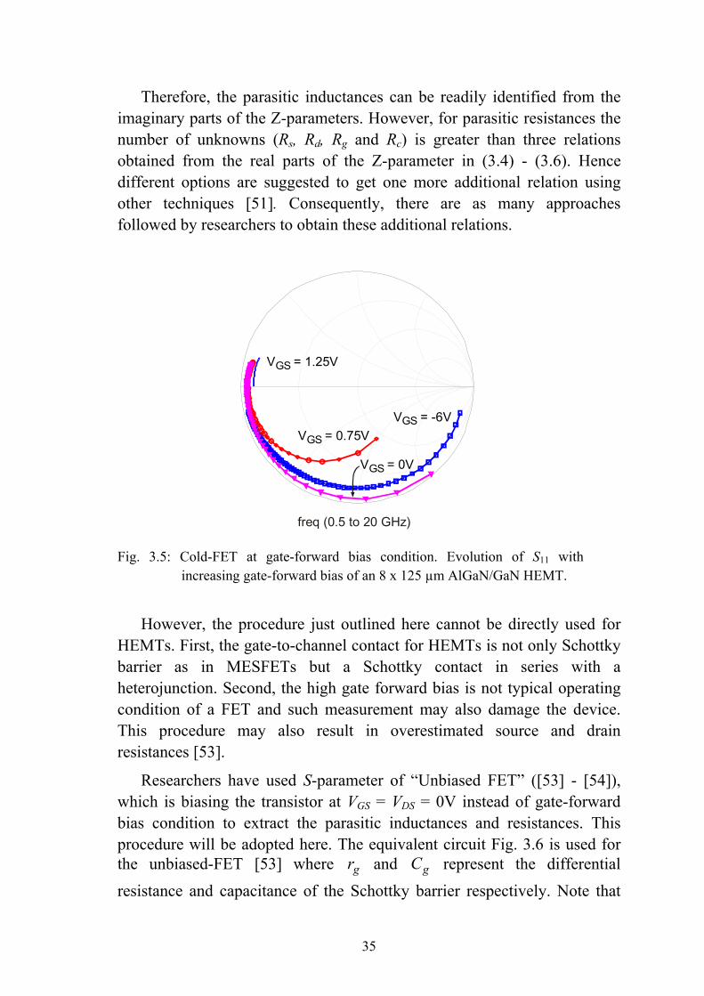
35
Therefore, the parasitic inductances can be readily identified from the imaginary parts of the Z-parameters. However, for parasitic resistances the number of unknowns (Rs, Rd, Rg and Rc) is greater than three relations obtained from the real parts of the Z-parameter in (3.4) - (3.6). Hence different options are suggested to get one more additional relation using other techniques [51]. Consequently, there are as many approaches followed by researchers to obtain these additional relations.
Fig. 3.5: Cold-FET at gate-forward bias condition. Evolution of S11 with increasing gate-forward bias of an 8 x 125 µm AlGaN/GaN HEMT.
However, the procedure just outlined here cannot be directly used for HEMTs. First, the gate-to-channel contact for HEMTs is not only Schottky barrier as in MESFETs but a Schottky contact in series with a heterojunction. Second, the high gate forward bias is not typical operating condition of a FET and such measurement may also damage the device. This procedure may also result in overestimated source and drain resistances [53].
Researchers have used S-parameter of “Unbiased FET” ([53] - [54]), which is biasing the transistor at VGS = VDS = 0V instead of gate-forward bias condition to extract the parasitic inductances and resistances. This procedure will be adopted here. The equivalent circuit Fig. 3.6 is used for the unbiased-FET [53] where gr and gC represent the differential resistance and capacitance of the Schottky barrier respectively. Note that
freq (0.5 to 20 GHz)
V = 1.25VGS
V = 0.75VGS
V = 0VGS
V = -6VGS

36
the parasitic capacitances ( pgC and pdC ) can be de-embedded from measured data. The Z-parameters of this equivalent circuit are:
⎟⎟
⎠
⎞
⎜⎜
⎝
⎛−+++++=
DrC
LLjDrR
RRZ ggsg
gcsg
2
11 2ω (3.8)
sc
s LjRRZZ ω++==22112 (3.9)
( )sdcsd LLjRRRZ ++++= ω22 (3.10)
where ( ) .2ggrCω1D += And now considering the gate Zg, source Zs, and
drain Zd branch impedances,
⎟⎟
⎠
⎞
⎜⎜
⎝
⎛−++=−=
DrC
LjDr
RZZZ ggg
ggg
2
1211 ω (3.11)
sc
ss LjRRZZZ ω++===22112 (3.12)
dc
dd LjRRZZZ ω++=−=22122 (3.13)
Fig. 3.6: Simplified small-signal equivalent of unbiased FET ( VV,VV DSGS 00 == ) (after [53]).
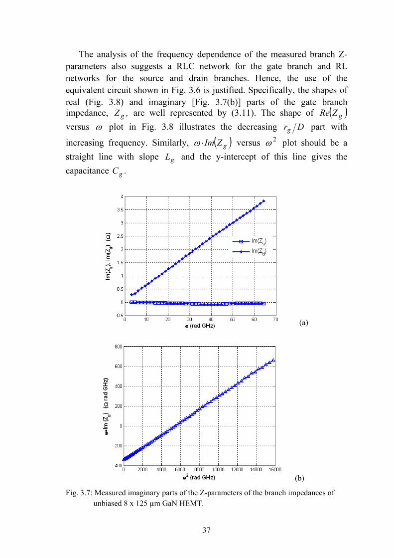
The analysis of the frequency dependence of the measured branch Z-parameters also suggests a RLC network for the gate branch and RL networks for the source and drain branches. Hence, the use of the equivalent circuit shown in Fig. 3.6 is justified. Specifically, the shapes of real (Fig. 3.8) and imaginary [Fig. 3.7(b)] parts of the gate branch impedance, ,Z g are well represented by (3.11). The shape of ( )gZRe versus ω plot in Fig. 3.8 illustrates the decreasing Drg part with
increasing frequency. Similarly, ( )gZIm⋅ω versus 2ω plot should be a straight line with slope gL and the y-intercept of this line gives the capacitance .Cg
Fig. 3.7: Mu
(a)
37
(b)
easured imaginary parts of the Z-parameters of the branch impedances of nbiased 8 x 125 µm GaN HEMT.

38
Table 3.1: Extrinsic parameters of 8 x 125 µm GaN HEMT based on small-signal EEC model in Fig. 3.2.
Cpg [fF] Cpd [fF] Rg [Ω] Rs [Ω] Rd [Ω] Lg [pH] Ls [pH] Ld [pH]
247 50.5 0.383 0.093 1.482 64 0.021 57.3
First, lets consider the imaginary parts of these branch impedances, as they are the simplest to identify. Both sL and dL are readily obtained from the slope of ( )sZIm and ( )dZIm plots respectively as shown in Fig. 3.7(a). However, sL turns out to be very small (0.021 pH). Whereas the low frequency reactance of ( )gZIm is dominated by the gate differential
capacitance gC , the slope of ( )gZIm⋅ω versus 2ω plot shown in Fig. 3.7(b) gives .Lg
Fig. 3.8: Measured real parts of the Z-parameters of the branch impedances of unbiased 8 x 125 µm GaN HEMT.
Now consider the real parts of the branch impedances of the above equation set and the plots in Fig. 3.8. One notes that gR can be obtained from the horizontal asymptote of ( )gZRe plot where Drg becomes negligible. The resistances 2cs RR + and 2cd RR + are also identified from ( )sZRe and ( )dZRe plots, respectively. And following a method described in [54], the sum gs RR + can be determined from ( )11ZRe of pinch-off data and hence one can then calculate sR , cR and dR in that

39
order. The extrinsic parameters determined so far are summarized in Table 3.1.
Comparison is also made between the different techniques used for determining the parasitic resistances from the S-parameters of gate-forward and unbiased bias conditions. These are summarized in Table 3.2 below based on equations sets (3.4) - (3.6) for the gate-forward and (3.11) - (3.13) for the unbiased FET.
Now comparing the results from the gate-forward and unbiased FET conditions, the values for 2cs RR + and 2cd RR + expressions are very similar as can be seen in the 3rd and 4th rows of these tables. The gate resistances from the gate-forward bias condition are significantly larger due to the differential gate resistance rg term.
Table 3.2: Comparison of parasitic resistances from gate-forward, unbiased, and below pinchoff biased cold-FET conditions of a 2 x 50 µm, 8 x 125 µm, and 8 x 250 µm GaN HEMTs.
(a) Gate-forward biased HEMT 2 x 50 µm 8 x 125 µm 8 x 250 µm Rg + rg – 6cR [Ω] 5.36 2.03 2.0Rs + 2cR [Ω] 6.82 0.87 0.47Rd + 2cR [Ω] 9.23 2.0 0.78
(b) Unbiased HEMT 2 x 50 µm 8 x 125 µm 8 x 250 µm Rg [Ω] 1.89 0.37 1.35Rs + 2cR [Ω] 6.48 0.85 0.49Rd + 2cR [Ω] 9.35 2.08 0.80
3.4.2 Intrinsic Parameters
The bias dependent intrinsic parameters were then extracted based on the extrinsic parameters already determined. The usual method of de-embedding the extrinsic elements and the analytical expressions for the intrinsic elements as described in [46] was followed. However, the following consideration was made to determine the gate-source, fsG , and gate-drain, fdG , diode differential conductances. These were first estimated from the low frequency real parts of the intrinsic Y-parameters [46] using )Re(Y- G i12fd = and fdi11fs G - )Re(Y G = . Since the frequency of the S-parameter measurement data used starts at 0.5 GHz, the gate-source and gate-drain diode conductance determined might be
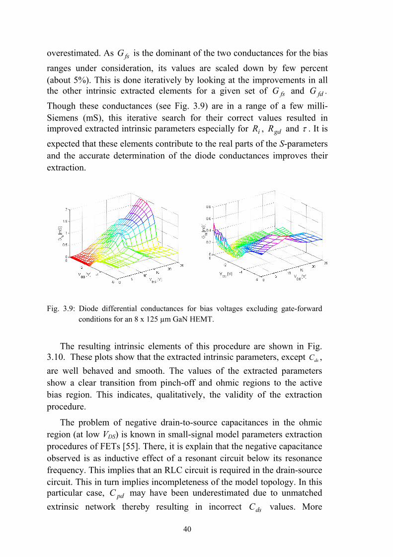
40
overestimated. As fsG is the dominant of the two conductances for the bias ranges under consideration, its values are scaled down by few percent (about 5%). This is done iteratively by looking at the improvements in all the other intrinsic extracted elements for a given set of fsG and .G fd Though these conductances (see Fig. 3.9) are in a range of a few milli-Siemens (mS), this iterative search for their correct values resulted in improved extracted intrinsic parameters especially for iR , gdR and τ . It is expected that these elements contribute to the real parts of the S-parameters and the accurate determination of the diode conductances improves their extraction.
Fig. 3.9: Diode differential conductances for bias voltages excluding gate-forward conditions for an 8 x 125 µm GaN HEMT.
The resulting intrinsic elements of this procedure are shown in Fig. 3.10. These plots show that the extracted intrinsic parameters, except dsC , are well behaved and smooth. The values of the extracted parameters show a clear transition from pinch-off and ohmic regions to the active bias region. This indicates, qualitatively, the validity of the extraction procedure.
The problem of negative drain-to-source capacitances in the ohmic region (at low VDS) is known in small-signal model parameters extraction procedures of FETs [55]. There, it is explain that the negative capacitance observed is as inductive effect of a resonant circuit below its resonance frequency. This implies that an RLC circuit is required in the drain-source circuit. This in turn implies incompleteness of the model topology. In this particular case, pdC may have been underestimated due to unmatched extrinsic network thereby resulting in incorrect dsC values. More
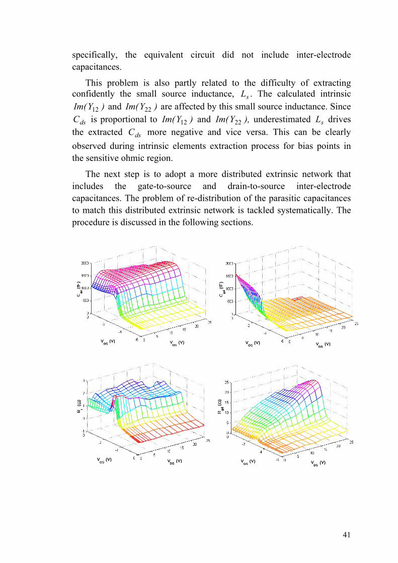
41
specifically, the equivalent circuit did not include inter-electrode capacitances.
This problem is also partly related to the difficulty of extracting confidently the small source inductance, sL . The calculated intrinsic
)YIm( 12 and )YIm( 22 are affected by this small source inductance. Since dsC is proportional to )YIm( 12 and ),YIm( 22 underestimated sL drives
the extracted dsC more negative and vice versa. This can be clearly observed during intrinsic elements extraction process for bias points in the sensitive ohmic region.
The next step is to adopt a more distributed extrinsic network that includes the gate-to-source and drain-to-source inter-electrode capacitances. The problem of re-distribution of the parasitic capacitances to match this distributed extrinsic network is tackled systematically. The procedure is discussed in the following sections.

42
Fig. 3.10: Extracted intrinsic parameters of an 8 x 125 µm GaN HEMT for extrinsic parameters listed in Table 3.1.
3.5 Modified Procedure for Extraction of Extrinsic Elements
It has been shown in previous section that the extracted intrinsic parameters based on the classical method are generally good. Hence, the starting points for improvement are to use variations of the standard procedures.
The main task remaining is to take into account the more complex structure of multi-finger HEMTs [see Fig. 3.11(c)]. In these HEMTs, the gate and drain fingers are bypassed with the air-bridge source interconnects. These source bridges are hanging at a few micrometers distance from the gate and drain fingers [Fig. 3.11(d)] and hence contribute significantly to extrinsic capacitances. These are distributed capacitances along the gate and drain fingers to the source. Since the

drain fingers are wider than the gate fingers, the drain-to-source inter-electrode capacitance, ,C pdi is expected to be greater than the gate-to-source inter-electrode capacitance, .C pgi However, the source bridge landings are on the gate fingers side, which makes the gate finger to source bridge separation distance smaller. Therefore, pgiC will also be considerable.
(a)
Fig
43
(c)
(b) (d)
. 3.11: Pictures of AlGaN/GaN HEMTs. 2 x 50 µm: (a) without and (b) with source bridge. (c) 8 x 125 µm. The gates are seen on the left side in all pictures. (d) A close-up picture of the source bridge interconnects from the drain side where the gate finger is seen close to the source than the drain [118].

44
For 2-finger HEMTs, the source bridge is not necessary [see Fig. 3.11(a)] and in that case the gate-source and drain-source inter-electrode capacitances are expected to be small due to the field through air path [16]. Even if there is a source bridge [Fig. 3.11(b)], the inter-electrode capacitance contribution with only two fingers is negligible compared to the pad capacitances thereby resulting in similar values of )Im(Y11 and
)Im(Y22 as discussed earlier [see Fig. 3.4(a)].
3.5.1 Improved Parasitic Network
The equivalent circuit adopted, shown in Fig. 3.12, is similar to the distributed model described in [50] and [56]. The pad capacitances are placed outermost which simplifies the extraction procedure by minimizing the number of impedance matrix inversions and improving the numerical accuracy [53]. Moreover, the resulting LC networks in L-configuration are good models for the gate- and drain-pads at low frequencies. Rosman et al. reported that these networks in L-configuration are valid up to 17 GHz for the pads they considered [57].
Starting with the results of the modeled and measured S-parameter of the 16-element equivalent circuit model of Fig. 3.2, one notes that the comparison between the S-parameter simulation and measurement (Fig. 3.13) is generally good except for 11S and ,S22 which are expected due to the neglected inter-electrode capacitances.
Fig. 3.12: 18-element small-signal equivalent circuit model including inter-electrode capacitances pgiC and pdiC arranged as a π-network with pad
capacitances pgaC and pdaC .

45
Therefore, the parasitic capacitance values found so far requires fine-tuning only. Hence, the following considerations were made in the optimization of parameters in ADS® using measured pinch-off S-parameter data. The key point in this procedure is the optimization of few parameters only at a time.
i) Only the branch capacitances partitioning is re-considered. The starting values of all known parameters are the values obtained from the 16-element equivalent circuit model in Fig. 3.2.
ii) In all steps, the gate-source, gate-drain and drain-source branch capacitances must add up to the total capacitances ω)YIm( 11 ,
ω)YIm( 12 and ω)YIm( 22 . The values of the parameters 0gsC and 0gdC (i.e. gate-source and gate-drain capacitances at pinch off) are restricted to vary within few percent (about ±10% maximum) of their starting values in order to avoid unphysical results. This is necessary in order to account for the unequal gate-source and gate-drain separation in the actual device layout. The gate is closer to the source than to the drain, and hence the fine-tuning is expected to produce 00 gdgs CC > . The conditions for optimization on the gate side are that only pgiC is optimized. But the maximum limits of
pgiC and at the same time, the sum pgipga CC + , are constrained to
0011
gdgs CC)YIm(
−−ω
. This step amounts to the partitioning of the
gate side capacitance to pgaC and pgiC . And on the drain side both
pdiC and pdaC are optimized with their maximum limits set to
022
gdC)YIm(
−ω
. The starting value of pdaC is set to the value
found with the standard procedure (i.e. pdC ). Again simultaneously, the sum dspdipda CCC ++ must be restricted to
022
gdC)YIm(
−ω
during the optimization. These steps basically
mean 0gsC and 0gdC are fine-tuned whereas the capacitances pgiC and pdiC are optimized within the constraints mentioned above.

46
Fig. 3.13: Comparison between simulation (lines) and measurement (Error < 8%) for pinched-off cold-FET with extrinsic parameters listed in Table 3.1 (8 x 125 µm GaN HEMT, VGS = -7V).
These steps result in the parasitic elements listed in Table 3.3 with the corresponding improved comparison between measurement and simulation shown in Fig. 3.14.
Table 3.3: Intermediate extrinsic and intrinsic parameter values of 8 x 125 µm GaN HEMT for the small-signal equivalent circuit model in Fig. 3.12.
Cpga [fF] Cpgi [fF] Cgs0 [fF] Cgd0 [fF] Cpdi [fF] Cpda [fF] Cds [fF]
143.6 102.2 288.2 261.0 128.1 112.4 97.5
iii) The last step is to consider reverse gate diode currents at such large negative gate bias voltages ( PGS VV < ). Diode conductances for the gate-source and gate-drain branches, represented by gsfR and ,Rgdf
2 4 6 8 10 12 14 16 180 20
0.88
0.90
0.92
0.94
0.96
0.98
0.86
1.00
ma
g(S
(1,1
))
2 4 6 8 10 12 14 16 180 20
0.90
0.92
0.94
0.96
0.98
0.88
1.00
freq, GHz
ma
g(S
(2,2
))
2 4 6 8 10 12 14 16 180 20
0.1
0.2
0.3
0.4
0.0
0.5
ma
g(S
(1,2
))
2 4 6 8 10 12 14 16 180 20
-150
-100
-50
-200
0
ph
ase
(S(1
,1))
2 4 6 8 10 12 14 16 180 20
-150
-100
-50
-200
0
freq, GHz
ph
ase
(S(2
,2))
2 4 6 8 10 12 14 16 180 20
-50
0
50
-100
100
ph
ase
(S(1
,2))

47
are added in parallel to 0gsC and 0gdC , which are then optimized. The starting values for capacitance values are set to those found in the previous step. The conditions for optimization are similar to step described in (ii) above except for the diode conductances, which are not restricted to minimum or maximum limits in their values.
Fig. 3.14: Comparison between simulation (lines) and measurement for pinched-off cold-FET with extrinsic parameters listed in Table 3.3 (8 x 125 µm GaN HEMT, VGS = -7V).
This last step results in the values of extrinsic parameters listed in Table 3.4. The comparison between measurement and simulation shown in Fig. 3.15 is good in both the magnitude and phase of the S-parameters.
2 4 6 8 10 12 14 16 180 20
0.90
0.92
0.94
0.96
0.98
0.88
1.00
freq, GHz
ma
g(S
(2,2
))
2 4 6 8 10 12 14 16 180 20
0.1
0.2
0.3
0.0
0.4
ma
g(S
(1,2
))
2 4 6 8 10 12 14 16 180 20
-150
-100
-50
-200
0
p
ha
se(S
(1,1
))
2 4 6 8 10 12 14 16 180 20
-150
-100
-50
-200
0
freq, GHz
ph
ase
(S(2
,2))
2 4 6 8 10 12 14 16 180 20
-50
0
50
-100
100
ph
ase
(S(1
,2))
2 4 6 8 10 12 14 16 180 20
0.88
0.90
0.92
0.94
0.96
0.98
0.86
1.00
ma
g(S
(1,1
))

4
Table 3.4: Optimized extrinsic and intrinsic parameters and diode conductances of 8 x 125 µm GaN HEMT for the small-signal equivalent circuit model in Fig. 3.12.
Cpga [fF] Cpgi [fF] Cgs0 [fF] Cgd0 [fF] Cpdi [fF] Cpda [fF] Cds0 [fF] Rgsf [Ω] Rgdf [Ω]
172.6 56 300 267.7 173.4 119.9 38.1 1823 2566
F
Ftier
A
0.96 0
8
ig. 3.15: Comparison between simulation (lines) and measurement for pinched-off cold-FET with extrinsic parameters listed in Table 3.4 (8 x 125 µm GaN HEMT, VGS = -7V).
Finally, the intrinsic elements were extracted. The results are shown in ig. 3.16, which demonstrate improved intrinsic parameters as function of
he grid voltages. The problem of negative drain-source capacitance, ,Cds n the linear region is now less dramatic. Again, the values of the xtracted parameters show a clear transition from pinch-off and ohmic egions to the active bias region.
We note that these plots have a typical characteristics observed for lGaN/GaN HEMTs. The intrinsic gate-to-source capacitance, gsC ,
2 4 6 8 10 12 14 16 180 20
0.88
0.90
0.92
0.94
0.86
ma
g(S
(1,1
))
2 4 6 8 10 12 14 16 180 20
0.90
0.92
0.94
0.96
0.88
0.98
freq, GHz
ma
g(S
(2,2
))
2 4 6 8 10 12 14 16 180 20
0.1
0.2
0.3
0.0
0.4
ma
g(S
(1,2
))
2 4 6 8 10 12 14 16 180 20
-150
-100
-50
-200
ph
ase
(S(1
,1))
2 4 6 8 10 12 14 16 180 20
-150
-100
-50
-200
0
freq, GHz
ph
ase
(S(2
,2))
2 4 6 8 10 12 14 16 180 20
-50
0
50
-100
100
ph
ase
(S(1
,2))

49
increases sharply with increasing gate bias voltage from its pinchoff value. This may be explained as follows [58]: gsC is located between the gate contact and the channel carrier density with the channel charge as a movable capacitor plate. As the gate voltage is raised above its pinchoff value, the charge density shifts closer towards the gate thereby increasing the capacitance. The variation mechanism of gsC with drain voltage is also similar at low drain voltage ranges.
The variation of the gate-drain capacitance, ,Cgd with drain voltage is explained by the extension of the depletion region into the gate-drain space. This extension increases with increasing drain voltage thereby reducing the gate-drain capacitance. One also notes that the intrinsic parameters ,Cgs gdC and dsC in pinchoff and low VDS bias regions are close to their values listed in table 3.3 above ( ,Cgs0 0gdC and 0dsC for ‘cold-FET’ and VGS = -7V).
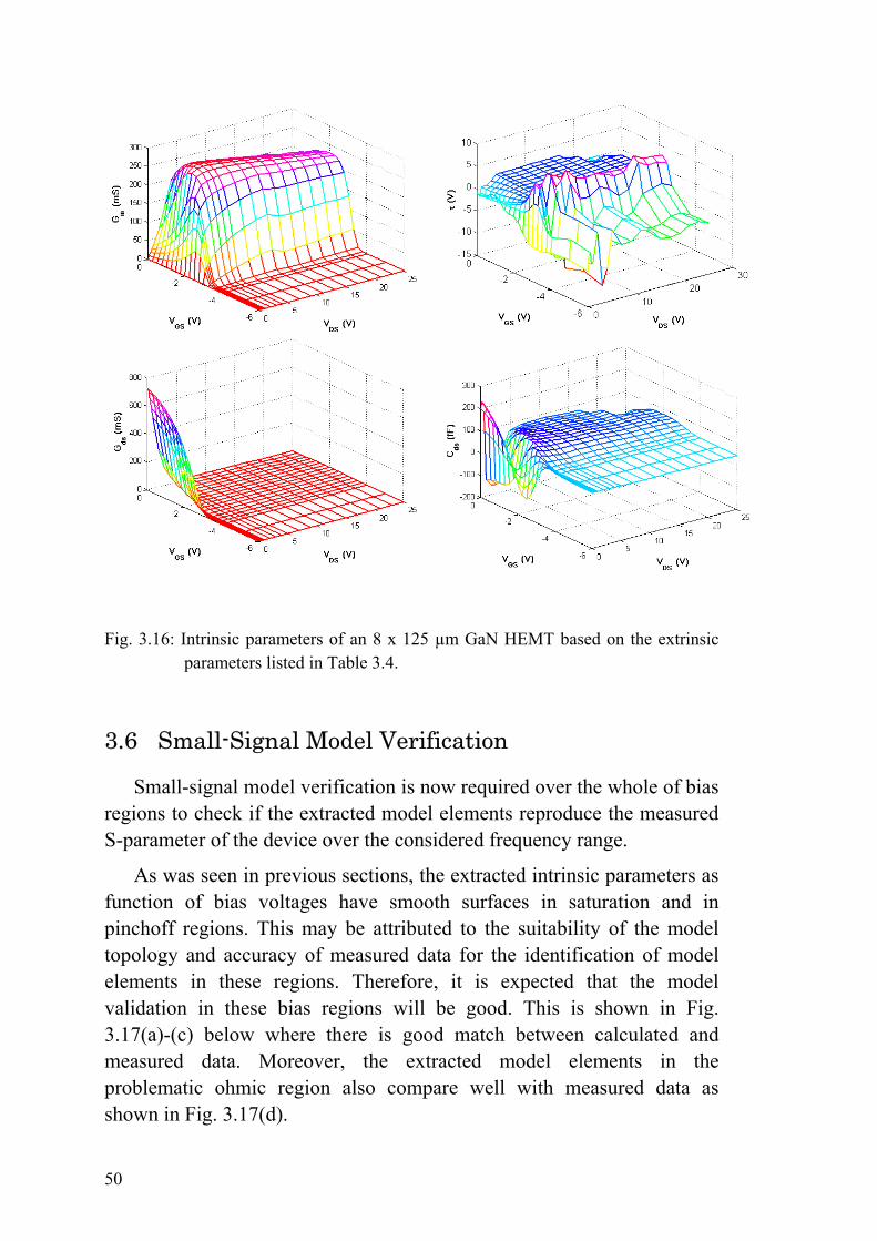
50
Fig. 3.16: Intrinsic parameters of an 8 x 125 µm GaN HEMT based on the extrinsic parameters listed in Table 3.4.
3.6 Small-Signal Model Verification
Small-signal model verification is now required over the whole of bias regions to check if the extracted model elements reproduce the measured S-parameter of the device over the considered frequency range.
As was seen in previous sections, the extracted intrinsic parameters as function of bias voltages have smooth surfaces in saturation and in pinchoff regions. This may be attributed to the suitability of the model topology and accuracy of measured data for the identification of model elements in these regions. Therefore, it is expected that the model validation in these bias regions will be good. This is shown in Fig. 3.17(a)-(c) below where there is good match between calculated and measured data. Moreover, the extracted model elements in the problematic ohmic region also compare well with measured data as shown in Fig. 3.17(d).

(a) (b)
(c)
Fig. 3.17: Small-signal model S-parameter vbias voltages (a) (VGS = -2V, VDS
are in saturation region while (c) 1V, VDS = 1V) are in pinchoff and
These comparisons of calculated aindirect indicators of the suitability accuracy of extrinsic element values.
S11
0.07xS21
S22
5xS12
freq (0.5 to 20 GHz) freq (0.5 to 20 GHz)
S11
0.07xS21
S22
5xS12
S11
-2xS21
-S22
2xS12
freq (0.5 to 20 GHz)
51
(d)
erification for 1 mm GaN HEMT. The = 25V) and (b) (VGS = -1.5V, VDS = 15V) (VGS = -5V, VDS = 15V) and (d) (VGS = -ohmic regions, respectively.
nd measured S-parameters are also of the extraction procedure and
S11
20xS21
S2210xS12
freq (0.5 to 20 GHz)

52
3.7 Nonlinear Voltage Referencing
The measured bias-dependent data (S-parameters and pulsed DC characteristics) are all functions of extrinsic voltages defined at the device terminals. Consequently, the extracted bias-dependent intrinsic model elements are referenced to these voltages. But these bias-dependent model elements have to be defined as function of the internal controlling voltages for model implementation in a nonlinear circuit simulator. This is done first by calculating the voltage drops across the extrinsic resistances as follows,
⎟⎟⎠
⎞⎜⎜⎝
⎛⎟⎟⎠
⎞⎜⎜⎝
⎛
+
+−⎟⎟
⎠
⎞⎜⎜⎝
⎛=⎟⎟
⎠
⎞⎜⎜⎝
⎛
DS
GS
dgs
ssg
DS
GS
ds
gs
II
RRR
RRR
VV
V
V (3.14)
where gsV and dsV are the intrinsic gate-source and drain-source voltages, respectively. For pulsed DC measurements and as per the definitions of
terms used, the pairs ⎟⎟⎠
⎞⎜⎜⎝
⎛
DS
GS
VV
and ⎟⎟⎠
⎞⎜⎜⎝
⎛
DS
GS
II
in static DC are replaced by
⎟⎟⎠
⎞⎜⎜⎝
⎛
DS
GS
vv
and ⎟⎟⎠
⎞⎜⎜⎝
⎛
DS
GS
ii
in pulsed DC measurements, respectively.
The calculated intrinsic voltages will not be on orthogonal grid and hence the corresponding model parameters should be transformed onto orthogonal grid using spline interpolation and/or extrapolation. The results can be then written into a file for look-up table implementation of the model in a nonlinear circuit simulator.
The other option is to leave the voltage referencing to the nonlinear simulator itself. One can implement these implicit nonlinear re-referencing equations for the extrinsic voltages directly in the nonlinear simulator [59]. The extrinsic voltages are calculated for a given sensed intrinsic voltages of the model by the simulator at run-time. This may influence the simulation speed, as these additional equations must be solved during simulation.

53
Chapter 4
Large-Signal Modeling of Power FETs
Nonlinear device modeling is a complex subject and it is even more challenging for power transistors whose technology has not been refined. Particularly, different physical processes result in complex device behavior for the new III-V based transistors. As the most important nonlinear model elements of a FET are the nonlinear charge and conduction current models, some of the problems related to their model derivation are reviewed in this chapter.
The chapter starts with the review of nonlinear device modeling approaches from the data base point of view. Next fundamental requirements of a nonlinear model for intermodulation distortion (IMD) simulation are summarized. As one of the problems related to nonlinear charge modeling is the consistency problem, a top-down modeling approach targeted to addressing this issue is also reviewed. A brief summary of this technique when applied to power AlGaN/GaN HEMTs will be presented.
The second part of the chapter is devoted to device characterization where pulsed DC and transient measurements will be treated. These measurements form the basis of the dispersive drain current model described in Chapter 5.
4.1 Data Base for Large-Signal Device Model
Large-signal modeling procedure may rely on data that are obtained from measurement or material parameters and physical process considerations. In the latter case, the physical data includes material properties (e.g.

54
bandgap energies, density of states and dielectric constants), carrier transport properties (electron mobility and saturated electron velocity) and the device geometry [60]. These are inputs to device simulators whose basic function is to solve simultaneously the Poisson and the current-continuity equations [60]. These equations are solved analytically or numerically and involve approximations to make the problem tractable. The approach followed depends on the trade off between accuracy, computation time and ease of use.
In many cases, however, the physical data is not readily available for the general circuit designer. This modeling approach is, therefore, limited mainly to device designers who have some control over the device fabrication process. For foundries, physical models are useful to predict circuit level performance without first fabricating the device.
Measurement based models use characterization techniques such as S-parameters and pulsed I-V data. These techniques are the most common and provide improved large-signal simulation accuracy because the model nonlinearities are constructed from measurements that emulate actual device application.
In general, the first step is the definition of the equivalent circuit topology of the device. This is necessary as the circuit simulators solve equations based on Kirchhoff’s current and voltage laws. The equivalent circuit models are derived with careful consideration of the physical layout of the device as seen in Chapter 3 for the small-signal equivalent circuit of a FET. The measurement data must be processed to extract the linear and nonlinear model elements of the equivalent circuit.
There are basically two ways to make use of the processed data in a nonlinear simulator. The intrinsic FET large-signal model elements may be approximated by standard analytical functions (and hence “analytical models”) or can be implemented in table form, which can then be interpolated and/or extrapolated. The latter are called “table-based” models and this technique will be implemented in this thesis.
The model implementations using analytical functions (e.g. [61]-[65]) are fast but can also be inaccurate. This is because it is difficult to find functions that fit globally the nonlinear device model parameters over large grid voltage range. This is the case, for example, for the new GaN HEMT with operating voltages of 50V or more. More sophisticated analytical equations with about 100 parameters have been recently reported for GaN

55
HEMTs [66]. The main advantages of using analytical functions include computational efficiency and the ability to simulate beyond measurement range due to better data extrapolation.
The table based model implementation is accurate and technology independent [67]. It is based directly on the measured data and hence no need to assume for any analytical function(s) that can fit the data of the nonlinear model element(s). However, the main problem with this technique is inaccuracies caused by interpolation and/or extrapolation errors. The interpolation problems appear when simulating the large-signal model at low power levels where the interpolated data may appear oscillatory [68]. The solutions to the problem include making the measured data available for denser grid and improved interpolation techniques such as “smoothing-splines” [69]. Unphysical extrapolation (e.g. cross-over of extrapolated I(V) characteristics) may also lead to model convergence problems. These are not fundamental limitation of table-based models but rather limitations in model implementation.
There are researchers working to develop hybrid model, which aims to combines the advantages of these two model implementation techniques [68]. In the hybrid model, continuously differentiable analytical functions can be fitted to nonlinear elements having well-behaved characteristics such as the isothermal drain-source current but use table-based data for nonlinear elements with more complicated characteristics.
There are also recent works that make use of the concept of neural networks for modeling of nonlinear devices and networks. As in other applications of this technique, the artificial neural network (ANN) is trained to learn the input-output relationship based on measurement data of the device. The input and output measurement data can be currents and voltages at set of frequencies, different power levels, and under different load conditions [70]. Hence, once the ANN “learns” the input-output relationship, the model output voltage and current can be calculated for any other input signal, including those not used for training the network.
4.2 Large-Signal Models for IMD Prediction
For accurate IMD simulations, the nonlinear model elements and their higher order derivatives must be modeled accurately [71]-[72]. This will be

56
evident from the discussion of a simplified FET equivalent circuit shown in Fig. 4.1 for an IMD analysis.
Additionally, for varying envelope frequency of a modulated signal, the IMDs are function of the envelope frequency. This frequency dependence of the IMD products stems from:
(a) Dispersive device characteristics. Obviously, the IMD is function of the device’s nonlinearity, which in turn depends on the device bias point. Since the bias point affects the state of traps and self-heating, the IMDs are functions of dispersion effects.
(b) Electrical environment outside the device. When device nonlinearities are terminated with impedances that are function of RF and envelope frequencies, the resulting IMDs are function of these frequencies. The aim of gate- and drain-bias circuits design, having nearly zeroed base impedances, is to solve this problem.
Accordingly, the investigations of both cases (a) and (b), through a successful simulation, demand a comprehensive nonlinear device model including temperature and trapping effects. In the following paragraphs, simplified literature review summarizes IMD analysis to give some more insight into the subject.
Fig. 4.1: FET circuit used in Volterra analysis (after [74]). The currents and voltages shown are the incremental values (excluding the bias voltages and currents) as described in [72].
The IMD performance of a FET is the product of the different nonlinearities of the transistor and the impedance environment presented to the FET. For broadband power amplifier applications, the IMDs are
vs idsCgs
Zg
igs
vgs Zdvds

57
affected by the impedances not only at the fundamental and higher harmonic frequencies, but also at the baseband frequencies.
There are some research works that attempted to come up with theoretical treatment of IMDs. These are mostly based on much simplified assumptions of the nonlinearities of the FET to make the problem amenable as there exists currently no theory of nonlinearity in large-signal circuits [73]. Nevertheless, these works give an insight to the complexity of the generated IMD and the so-called memory effect. As an example, a simplified analysis for the intermodulation level of the drain voltage at the output of a FET (Fig. 4.1) is summarized below [74].
This simplified equivalent circuit is an approximation of a FET biased in saturation region where the gate-source and drain-source current only are considered nonlinear. The Taylor-series expansions of these nonlinearities up to the third order are [72], [74],
33
22
22
33
22
22
dsddsgsmddsgsdmgsm
dsddsgsmdgsm
dsdsgsmdsgsds
vGvvGvvGvG
vGvvGvG
vGvG)v,v(i
++++
+++
+=
(4.1)
2321 32 gsgsgsgsgsgsgs vCvCC)v(C ++= (4.2)
( )33
221 gsgsgsgsgsgsgs vCvCvC
dtd)v(i
gs++= (4.3)
where the Taylor-series expansion coefficients in (4.1) are the derivatives of the drain-source current at a given bias point as described in [72]. Gm
and Gds are linear transconductance and output conductance. Gm2 and Gm3 describe the transconductance variation with gate-source voltage. Similarly, Gd2 and Gd3 describe the output conductance variation with drain-source voltage. The cross-terms Gmd and Gm2d represent the first and second order nonlinear dependence of Gds on gate-source voltage. Similarly, the cross-terms Gmd and Gmd2 represent the dependence of Gm on drain-source voltage.
A simplified analysis of the FET circuit for intermodulation level of the drain voltage under a two-tone excitation results in [74],

58
( ) ( ) ( ) ( )[ ]c*
csd ZccZcrrZVV ωωωωωω 22 02121002
03
213 ++−=− (4.4)
( ) ( ) ( ) ( )[ ]c*
csd ZccZcrrZVV ωωωωωω 22 02112002
03
123 ++−=− (4.5)
where
)(Z||G)(Z dd ωω 10
−= (4.6)
)(ZGA cm ω0−= (4.7)
)(ZCjr
cggsc ωω 111
+= (4.8)
( )[ ] ( )AGGAAGAAGGc dmd*
d*
mdm 2220 221
21
+⎭⎬⎫
⎩⎨⎧ +++= (4.9)
( ) ( ) ⎥⎦⎤
⎢⎣⎡ +++++−= *
d*
md*
dmm AAGAAAGAAGGc 23
22231 2
312
31
43
(4.10)
( ) ( )*dmddmdm AGGAGAGGc 2
2222 2
41
+++= (4.11)
( )213 2 ωω −dV and ( )123 2 ωω −dV are the lower, IMD3L, and upper, IMD3U, intermodulation drain voltages, respectively. sv is the two-tone excitation with the lower and upper tones at 1ω and ,2ω respectively. Further, it is assumed that the difference frequency, ,12 ωω − is small compared to the mid band carrier frequency, ,cω so that
.c 211221 22 ωωωωωωω −≈−≈≈≈
Hence, the r term is due to the gate-source capacitance nonlinearity. 0c , 1c and 2c are functions of the nonlinearities of the drain current at the
bias point and the effective drain impedance, ),(Z cω0 but independent of the difference frequency. 1c is function of the third-order transconductance and conductance and the cross terms whereas 0c and 2c are functions of second-order transconductance and conductance and the cross terms.
Both IMD3L and IMD3U are composed of distortion terms (i.e. vector sums) that depend on the third-order ( 1c ) and second-order [ )(Zc 1200 ωω − and )(Zc cω202 ] terms. Hence, the third-order

59
nonlinearity is augmented by distortions contributed by the product of the second-order drain current nonlinearities and the impedances at baseband and second harmonics. Moreover, the IMD3L and IMD3U in (4.4) and (4.5) differ due to the presence of different baseband impedance terms [ )(Z 120 ωω − and its conjugate )(Z 210 ωω − ]. Therefore, these cause differences in the magnitude and phase of the resultant IMD3L and IMD3U. The representation of these IMD3 products in a vector diagram is shown in Fig. 4.2 where the phase reversal in the second-order terms due to the baseband impedance is illustrated. Nothing that the above analysis is a highly simplified one, the IMDs in reality are the resultant of several vectors and depend on the DC bias and the drive level.
Fig. 4.2: IMD3 Composition for a transistor modeled by 3rd order polynomial (after [75]).
The composite IMD3 vectors (Fig. 4.2) have varying magnitude and phase with varying modulation frequency of the input signal if the impedances at baseband, fundamental and/or harmonic frequencies are bandwidth dependent. This is true even for fixed input signal levels. Practically, it is the impedance at baseband frequency that is highly bandwidth dependent [12]. The IMD magnitude and phase variation with the envelope frequency of the input signal is termed as memory effect. Such an IMD is quite difficult to cancel using linearization techniques such as a predistorter mainly because of its varying phase (φL and φU in Fig. 4.2). Therefore, the performance of the predistorter linearizers degrades in the presence of memory effects, as the predistorter should be optimized for given amplitude and phase of an IMD [76].
2nd order(harmonic)
Composite IM
D Vector
Lower IMD3 Vector
2nd order(envelope)
φL
3 o
rder
rd
2nd order(harmonic)
Compo
site
IMD V
ector
Upper IMD3 Vector
2nd order(envelope)
φU
3 o
rder
rd

60
The solution to the problem can be to minimize the impedance presented to the FET at the baseband frequencies. In this regard, the design of bias networks with sufficiently low impedances at baseband frequencies has become important. This is an important step in an effort to reduce memory effects. The resulting quasi-memoryless power amplifier would be amenable to linearization techniques.
The memory effect just described is related to varying impedances as function of the modulation envelope frequencies. But the device nonlinearities are also source of memory effects. One such effect is related to dynamic self-heating and/or ambient temperature variations. For example, under multi-carrier signal operation, the temperature of the device is modulated by the envelope frequency of the multi-carrier signal. Since most of the nonlinearities of the device are functions of the instantaneous junction temperature, the distortions generated become function of modulating envelope frequencies and hence source of memory effects. Trapping effects also have similar contributions to the memory effect.
In summary and relevant to the large-signal model of the FET for accurate prediction of the IMDs, the main nonlinear model elements must account for both thermal and trapping related effects and they should have accurate higher order derivatives.
4.3 Top-Down Modeling
In this section, an earlier research work at department of High Frequency Engineering that attempted to address the consistency and dispersion problems will be revised [77]. Specifically, a recent application of this technique to AlGaN/GaN HEMTs to solve consistency problem will be summarized.
The central issue in top-down large-signal modeling approach is addressing the problem of model consistency [77]. The problem stems from the fact that the traditional large-signal modeling techniques are based on first deriving a bias-dependent small-signal equivalent circuit for the intrinsic transistor which is then used to derive the large-signal model. This bottom-up approach introduces inconsistencies between the large-signal and small-signal models.
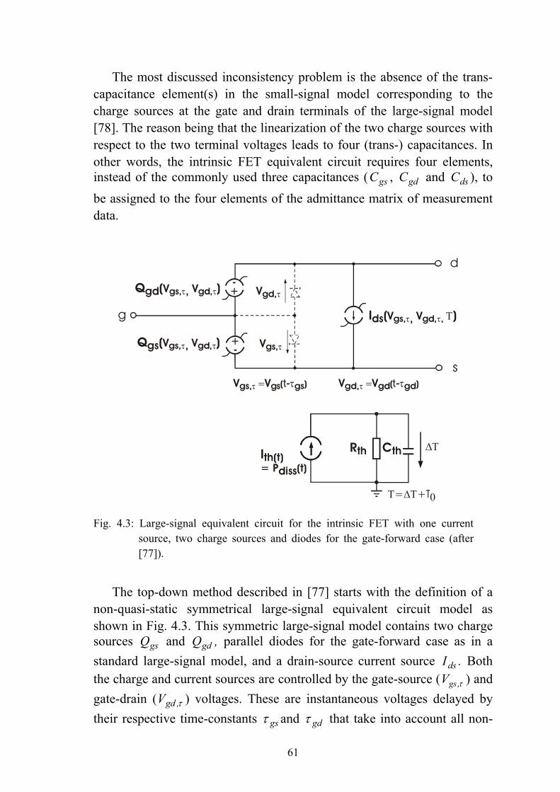
61
The most discussed inconsistency problem is the absence of the trans-capacitance element(s) in the small-signal model corresponding to the charge sources at the gate and drain terminals of the large-signal model [78]. The reason being that the linearization of the two charge sources with respect to the two terminal voltages leads to four (trans-) capacitances. In other words, the intrinsic FET equivalent circuit requires four elements, instead of the commonly used three capacitances ( gsC , gdC and dsC ), to be assigned to the four elements of the admittance matrix of measurement data.
Fig. 4.3: Large-signal equivalent circuit for the intrinsic FET with one current source, two charge sources and diodes for the gate-forward case (after [77]).
The top-down method described in [77] starts with the definition of a non-quasi-static symmetrical large-signal equivalent circuit model as shown in Fig. 4.3. This symmetric large-signal model contains two charge sources gsQ and ,Qgd parallel diodes for the gate-forward case as in a standard large-signal model, and a drain-source current source .Ids Both the charge and current sources are controlled by the gate-source ( τ,gsV ) and gate-drain ( τ,gdV ) voltages. These are instantaneous voltages delayed by their respective time-constants gsτ and gdτ that take into account all non-
d
s
g I ( )ds V , Vgs, gd, , τ τ Τ
Q ( )gd V , Vgs, gd,τ τ
Q ( )gs V , Vgs, gd,τ τ
Vgd,τ
Vgs,τ
V V -gs, gs( gs)τ = τt V V -gd, gd( gd)τ = τt
+-
+-
Ith(t)= Pdiss(t)
Rth Cth ∆Τ
Τ ∆Τ 0= +T

62
quasi-static effects ( iR , gdR and τ in the standard small-signal models). By introducing these two time-delays for their respective voltages, the asymmetry introduced by τ in the standard small-signal equivalent circuit is overcome. This symmetric model with respect to the gate electrode permits to interchange drain and source terminals for device reverse operation.
Now, in order to use the large-signal model practically, the two-dimensional voltage dependencies of the current and the charge state functions have to be determined. However, the charge state functions cannot be experimentally determined from measurements. The normal approach is to relate the derivative of the state functions to the intrinsic small-signal measurements. The measured small-signal quantities can be related to the parameters derived by linearization of the large-signal equivalent circuit at every bias point. The linearization as described in [77] results in 8 intrinsic elements ( HFsG , , HFdG , , ssC , , ddC , , dsC , , sdC , , gsτ and gdτ ) that can be related to the measured four complex intrinsic Y-parameters. Therefore, it is possible to analytically solve directly for these 8-intrinsic model elements at each frequency and bias point.
Fig. 4.4: Small-signal equivalent circuit of the large-signal model in Fig. 4.3. The currents through the capacitances are delayed by their respective time constants gsτ and gdτ .
The small-signal equivalent circuit corresponding to the large-signal model of Fig. 4.3 is shown in Fig. 4.4. One notes that this small-signal model contains trans-capacitance elements, dsC , and ,,sdC corresponding

63
to the partial differentials of the charge sources to the remote terminal voltages; namely gdgs VQ ∂∂ and ,gsgd VQ ∂∂ respectively.
Thus knowing the small-signal model parameters at each bias point, the large-signal state functions gsQ and gdQ can be obtained by path-independent integration if the integrability condition is satisfied [77].
∫
∫
⎟⎟⎠
⎞⎜⎜⎝
⎛−+=
⎟⎟⎠
⎞⎜⎜⎝
⎛=
V
BV ds
gsd,ss,sd,s
V
BV gd
gsd,ss,sgdgsgs
dvdv
)C,CC(
dvdv
)C,C()V,V(Q
r
r
r
r
(4.12)
and
∫
∫
⎟⎟⎠
⎞⎜⎜⎝
⎛−+=
⎟⎟⎠
⎞⎜⎜⎝
⎛=
V
V ds
gsddsddd
V
V gd
gsddsdgdgsgd
B
B
dvdv
CCC
dvdv
CCVVQ
r
r
r
r
),(
),(),(
,,,
,,
(4.13)
where the vector ),( dsgs VVV =r
and BVr
is the integration starting point.
The integrability condition, for the charge state functions to be independent of the integral path, requires that the intrinsic admittance data satisfy the following [67].
( ) ( )gs
dsgsdata
ds
dsgsdata
VVVY
VVVY
∂
∂=
∂
∂ ωω ),(Im),(Im 1211 (4.14a)
( ) ( )gs
dsgsdata
ds
dsgsdata
VVVY
VVVY
∂
∂=
∂
∂ ωω ),(Im),(Im 2221 (4.14b)
As mentioned earlier, the main motive to develop this new large-signal model is to solve the problem of consistency seen in the traditional modeling techniques. However, the application of this modeling technique to AlGaN/GaN HEMTs turns out to produce intrinsic elements, which are highly frequency dependent. This is particularly severe for extraction of the small-signal model elements in ohmic and pinch-off bias regions of the device. Fig. 4.5, for example, shows frequency dependence of sample

64
small-signal model elements for an active bias point. Clearly, these intrinsic elements are highly frequency dependent, which is an indication of model topology mismatch as compared to the actual device operation. This is partly due to a high sensitivity of the analytic equations of the small-signal model elements to measurement data. Particularly, the separation of the branch capacitances into their capacitance and transcapacitance elements ( ssC , and dsC , or ddC , and sdC , pairs) is highly sensitive to frequency. These elements are inversely proportional to frequency but with opposite sign. The equations of these intrinsic elements indicate that the pairs ssC , and sdC , are inversely proportional to frequency at low frequencies.
Generally, with good extrinsic (parasitic) parameters estimation and a matching model topology, the extracted intrinsic elements are ideally frequency independent [79]. This is not the case for the small-signal model just discussed.
The second important issue addressed, also in top-down modeling technique, is the modeling of the deviations between the static and dynamic drain current characteristics (low-frequency dispersion phenomenon). This has been dealt with by using ‘backgating’ approach, which is similar to the works in [80] and [81]. The ‘backgating’ model in [77] is based on static drain current characteristics and standard S-parameters measurements. As pointed out in [80] and a related discussion of this approach in next chapter, this method is less accurate as compared to empirical models based on pulsed DC characteristics in predicting the drain current dynamic deviations over wider range of quiescent bias conditions. This is because the ‘backgating’ concept is an indirect way of modeling the deviation between the dynamic and the static drain current characteristics using an equivalent gate voltage.
One notes that model consistency problem may be viewed separately from the low-frequency dispersion modeling of the drain current. Hence, the drain current based on pulsed DC measurements can be implemented in the top-down modeling technique reviewed above. But, the problems in the small-signal model elements extraction discussed above must be solved first.

65
Fig. 4.5: Small-signal intrinsic model elements (Top-down model for 8 x 125 µm GaN HEMT). Bias: (VGS = -2V, VDS = 17V).

66
4.4 Device Characterization
Device characterization is one of the initial and most important steps in device modeling process. The level of model accuracy depends on the characterization techniques employed and the accuracy of the measurement data. In fact, the nonlinear modeling technique followed is partly dictated by the possible measurement system available at one’s disposal. In general, the common measurement data types used as input to device modeling process are standard CW S-parameters, pulsed S-parameters with pulsed bias and pulsed I(V) characteristics.
Accurate and appropriate device characterization is also important for device diagnosis during fabrication process. In this regard, pulsed DC measurements are very useful for checking dispersion effects in power transistors. For example, “return” pulsed current technique has been used to compare the relative level of current collapse in AlGaN/GaN HEMTs [82]. In this technique, the device is biased in saturation region at (VGS0 = 0V, VDS0) where the drain-source bias VDS0 is kept fixed while the gate is pulsed from the 0V quiescent bias. Hence, a DC drain current of IDS0 flows with no gate pulse vGS applied. Next the amplitude of vGS is varied between 0V and a value below threshold voltage of the device. The corresponding “return” current, which is the drain current immediately after the gate pulse returns to vGS = 0V, is then measured. For a non-dispersive device, the drain current returns to its DC value IDS0 after vGS returns to 0V. But for a dispersive device, it takes certain time for the drain-current to recover to its DC value when the gate pulse returns to vGS = 0V. Therefore, the difference between the measured “return” current and IDS0 has been used as a measure of current collapse [37].
For developing a complete large-signal model that is useful for simulation of important DC and RF device properties, several types of device characterizations are required. In this regard, the new trend for characterization of power transistors is using pulsed DC I(V) and pulsed S-parameters measurements. However, few laboratories can afford these complete expensive measurement systems. Therefore, priorities are usually set in the modeling process as to which of the main device nonlinearities should be modeled to the best possible accuracy. As the main nonlinearity of a transistor is its drain current, the main focus is to characterize it accurately. To this end, pulsed DC I(V) measurement systems have been developed. This enables, among others, to characterize trapping and self-

heating effects separately. With pulsed measurement setup, it is possible to obtain RF characteristics at a fixed and controlled temperature.
Fig. 4
Rcharagenedata.rangeshow
(a)
67
(b)
.6: (a) RF loadlines at different drain voltage bias points superimposed on pulsed DC I(V) characteristics with negligible trapping and thermal effects (VGS0 = 0V, VDS0 = 0V). (b) RF loadlines superimposed on pulsed I(V) curves which are pulsed from the same bias points as the RF measurements (after [83]).
ecent experimental work supports the idea that pulsed I(V) cteristics are better suited for modeling the drain-source current
rator of a dispersive power device than the conventional S-parameter The experimental investigation has shown that the RF loadline swing correlates well with the pulsed I(V) characteristics [83]. As will be n later for GaN HEMTs, the pulsed I(V) characteristics show

68
increasing knee voltage and current collapse as the quiescent bias drain voltage is increased. Similarly, the experiment just mentioned showed that the RF loadline swing also shifts in the same direction as the drain bias voltage is increased. Fig. 4.6(b) shows the plots of RF loadlines at different drain bias points superimposed on pulsed DC I(V) curves measured from the same bias points as in the RF measurement. The increase in the knee voltage and decrease in drain current (current collapse) of the pulsed DC I(V) curves correlates with a similar shift of the RF loadlines at increasing drain bias voltages.
In this thesis, pulsed DC I(V) and multi-bias CW S-parameter characterizations are used for developing the large-signal model for AlGaN/GaN HEMTS on SiC substrates. The parasitic elements and the charge sources in the nonlinear models are obtained from data processing of the S-parameters. In doing so one assumes that dispersion effects on the intrinsic nonlinear capacitances are negligible. This is justified for the AlGaN/GaN HEMTs on SiC under consideration, which are 2 mm or less in size. The good thermal conductivity of SiC substrate makes the heat conduction efficient. Therefore, for devices of these size, the self-heating effects are not pronounced as can be seen from their static DC I(V) characteristics (see Fig. 3.1). Consequently, the S-parameter measurement at a given bias point will not be affected drastically by the self-heating. However, pulsed S-parameter measurements are necessary for devices of similar size but with poor thermal management. This is the case, for example, for AlGaN/GaN HEMTs on Si and sapphire substrates. In one study [84], two AlGaN/GaN HEMTs of identical structure built on SiC and sapphire substrates were investigated. The comparison of their DC I(V) characteristics shows that the GaN HEMT on SiC delivers twice current as compared to the GaN HEMT on sapphire. Hence the type of substrate has dramatic effect on the thermal performance of the device. This in turn dictates whether CW S-parameters are adequate or pulsed S-parameter measurements are necessary.
The discussions in following sections focus mainly on details of pulsed I(V) and transient measurements. These device characterizations provide us with the required and the main data for developing a dispersive electrothermal large-signal model of a power transistor.

69
4.4.1 Pulsed DC Measurement
In addition to the characterization of dispersion effects, pulsed DC technique enables also to perform measurements at power levels higher than those that can be tolerated continuously without destroying the device. This makes it possible for tests outside the safe operating area (SOA). Moreover, pulse transient measurements are required to obtain other important power device’s large-signal model parameters such as trapping and thermal time constants. It may also be used to determine breakdown characteristics.
The measured pulsed I(V) characteristics must exclude reactive currents related to charge variations. This is possible if the current is measured at a rate fast enough to exclude dispersion effects but also slow enough to exclude reactive currents. This is equivalent to saying that the frequency range of the measured current is above the cut-off frequencies of dispersion effects but well below the frequencies where reactive phenomenon related to charge variations and transit time of charges can be neglected [85]. This is illustrated in Fig. 4.7, which is a general form of the response of a FET to an ideal voltage step with a fast rise time [33]. The initial phase is the turn on transient, which contains the adjustment of the fast processes to the new voltages and the pulse may also include some ringing. The fast transport processes occur typically within ten picoseconds [33]. For example, the bias-dependent time delay τ for the 1 mm GaN HEMT extracted for the small-signal equivalent circuit in Chapter 3 is less than 5 ps (see Fig. 3.16). The approximate time for this initial phase is the inverse of the cut-off frequency (fT) of the device [33]. In phase II, the fast processes have adjusted to the new dynamic voltage level but the slow processes have not changed from the quiescent bias condition. The slow processes, which evolve charge exchange at the surface and in deep levels and electrical changes arising from heating (or cooling), adjust to the new voltage conditions in phase III. Phase IV corresponds to the steady-state (DC) current that is measured when the adjustment to the dynamic condition is complete.
Hence, the drain current sampling is taken during phase II in pulsed DC I(V) measurements. In transient current measurements (see section 4.4.3), the current curve in phase II and III are traced.

70
Fig. 4.7: General form of device current transient response to a voltage step (after [33]). The current in region III may decrease (as shown here) or increase depending on the selected quiescent bias and the “pulsed-to” points (see Fig. 4.11 and Fig. 4.13).
4.4.1.1 System Requirements
For characterization of a three terminal device like a power FET, a dual-pulse instrument is required. In dual-pulse system, fast-synchronized voltage pulses are applied to the input and output of the device from some reference quiescent bias voltages. The current response at the input and output of the device is then sampled at the end of the pulse.
A simple single pulse (“gate-lag”) type instrument [33] would not suit the purpose here since for AlGaN/GaN HEMTs (and many other devices) the states of the quiescent gate and drain voltages highly influence the measured drain-current. In typical single pulse systems, the device is biased at or below pinchoff while the drain is set at the desired DC. Then a fast pulse is applied from the gate side only so as to turn on the device and the drain current is then sampled. Hence, in single pulse system, the drain voltage can only be measured from pre-set DC values and it is not possible to pulse it from an arbitrary DC quiescent bias point.
For AlGaN/GaN HEMTs under consideration, drain pulse voltages in the range of 50V or more are required as these power devices can be operated at an even greater drain voltages. These power devices also have

71
maximum drain current, Imax, of about 1 A/mm and hence the current range of the pulse instrument must also be several amperes.
The other required important system attributes are the ability to pulse both positive and negative polarity and pulse widths in sub-microsecond range. The pulses need to be shaped so to avoid leading and trailing spikes. Of these, the most difficult to meet is the narrow pulse width requirement. Practical measurement constraints put limits to the minimum pulse width that can be set for reliable measurements. Specially, the unavoidable connecting cables for on wafer measurements add delays to the applied pulse [33].
Computer control software should properly control the sequence of the applied gate and drain pulses. The current and power dissipation limits should also be properly sensed.
Another practical problem in pulsed DC measurement system is the error introduced by the analog-to-digital converter (ADC) nonlinearity to the gate and drain voltage settings. It may not be necessary here to dwell on the hardware causes of the problem but the effects can be tested. Specially, the resolution of the gate voltage setting is of great concern since the drain current is sensitive to its slight variations from the intended values. Appendix A summarizes the result of tests on two instrument models of a pulsed DC system.
4.4.1.2 External Temperature Controller
One of the most distinct features of the new AlGaN/GaN HEMTs is their high power density. For high power devices (RF power > 10W) typical power densities are about 5 W/mm at 2.14 GHz for AlGaN/GaN HEMTs as compared to about 0.7 W/mm for Si-LDMOS and GaAs FETs [14]. This implies that the large RF power generated in a relatively small size causes considerable self-heating. Therefore, best estimate of the channel temperature is desired for accurate device model development.
The drain current model as function of channel temperature can be derived from pulsed I(V) measurement at different chuck temperatures. More specifically, to separate self-heating from trapping effects, pulse measurements from quiescent bias point (VGS0,VDS0) = (0V,0V) are necessary at different chuck temperatures. Moreover, the measurement of pulsed I(V) characteristics with varying chuck temperatures also enables to

72
determine the thermal resistance of the device structure. These conditions demand the availability of a suitable chuck temperature controller.
The pulsed DC measurement setup used in this work consists of a CASCADE probe station (Model 42), which is equipped with a hot chuck that allows variation of the base temperature from room temperature up to 200°C.
4.4.1.3 Characterization of Dispersion Effects
As discussed earlier, the central idea in using pulsed DC system is to make current measurements that enable to characterize self-heating and trapping effects. However, it is necessary to have a procedure to separately characterize these effects.
A complete set of dynamic I(V) characteristics is obtained by making dynamic I(V) measurements from a quiescent bias point ( )00 DSGS V,V to multiple pulsed-to points ( )DSGS v,v . This is illustrated in Fig. 4.8. The dynamic pulsed-to points, ( )DSGS v,v , are represented by the arrows from the bias point marked by ‘+’ sign.
The trapping and self-heating effects are both functions of the quiescent bias point ( )00 DSGS V,V . Obviously self-heating is significant only in active bias regions of non-zero drain current. In general, the pulsed I(V) characteristics of the HEMT is a function of the bias point ( )00 DSGS V,V , the pulsed-to point ( )DSGS v,v and channel temperature chT which may be written as,
( )chDSGSDSGSDS T,V,V,v,vfi 00= (4.15)
Thus the drain current is not only dependent on the instantaneous operating voltages ( )DSGS v,v but also upon the steady bias voltages ( )00 DSGS V,V . The channel temperature, chT , depends on the self-heating and the ambient temperature. Consequently, the pulsed I(V) characteristics from one particular bias point will be unique. In other words, there are theoretically infinite sets of dynamic I(V) characteristics of a FET that can be measured by varying the quiescent bias voltages. Practically, certain ranges of quiescent bias points that may be encountered for circuit operation (say Class AB, B and C) are of interest. Obviously, a set of

73
representative dynamic I(V) characteristics should be selected systematically in a practical large-signal modeling procedure.
Fig. 4.8: Illustration of pulsed I(V) measurement of a transistor. Synchronized positive and negative gate and drain pulses superimposed on the quiescent bias voltages are required to cover the voltage space.
The pulsed DC from quiescent bias point )VV,VV( DSGS 00 00 == may be assumed to have negligible trapping effects. In this bias condition, the electric field is small and the traps are not occupied. The current measured under this bias condition represents the maximum potential of the device under high frequency operation if traps and thermal problems can be solved to minimum level. In fact this current can be taken as reference in the modeling procedure of a dispersive drains-source current which is then modified by bias-dependent functions describing the thermal and trap effects [86].
The pulse characteristics used in the characterization of trapping and thermal effects, as presented in the following sections, have a pulse width of 1 µs or less and a repetition rate of 1 kHz. The duty cycle is, therefore, 0.1% or less so that a significant self-heating of the device due to the synchronized gate and drain pulses is prevented during the pulsing period. In other words, the self-heating of the device is determined exclusively by the selected quiescent bias point.

74
4.4.1.4 Charge Trapping
The technique to separately characterize trapping effects that excludes thermal effects is to make dynamic I(V) measurements at constant temperature of the power device. The measurements are performed from several quiescent bias points that have negligible or the same power dissipation (same dissipated power hyperbola). These bias points can be in the pinch-off region or on bias points along a constant power dissipation curve in the active bias region. Since the self-heating remains constant in these conditions, the differences seen in the dynamic I(V) characteristics from these bias points are attributed to charge trapping effects.
It is even possible to study the contribution of surface and buffer layer traps separately by using specific quiescent bias points. For example, trapping effects due to surface state can be studied by pulsing from quiescent bias points having different gate-source voltages but keeping drain-source voltage zero. This is based on the assumption that the surface traps and deep-level traps are mainly function of the gate voltage and the drain-source bias voltage, respectively [87].
As will be discussed in Chapter 5, the derivation of the parameters of a dispersive drain current model requires a set of pulsed I(V) datasets. This dispersive model needs to represent the current in (4.15) accurately. One of these techniques, described in [88], requires at least four dynamic I(V) datasets to identify its four model parameters. The quiescent bias points for these dynamic measurements are chosen strategically by taking into consideration surface and buffer trapping as well as self-heating effects.
Consequently, trapping effects due to surface states can be characterized by pulsing from quiescent bias points having different gate-source voltages but keeping drain-source voltage fixed or zero, ( )VVDS 00 = . The dissipated power at these bias points is negligible. The gate bias voltage differences between the bias points must be large enough to see significant changes in the drain current due to the surface traps. For the 1 mm GaN HEMT under consideration having a pinch-off voltage of about ,V.VP 54−= a bias voltage below pinch-off, ( )VV,VV DSPGS 000 =< , and a second at zero bias, ( )VV,VV DSGS 00 00 == , were chosen. The I(V) characteristics from these bias conditions are shown in Fig. 4.9(a). The decrease in pulsed DC drain current from the ( )V,V 07− bias as compared to from ( )V,V 00 bias point reveals the effect of the surface traps. One also notes that there is insignificant knee voltage increase.

75
Similarly, buffer trapping can be characterized making pulsed I(V) measurements from different drain bias conditions where gate bias is kept constant and dissipated power is negligible. But in this case a fixed gate voltage of VVGS 00 = cannot be used as this puts the bias point in active region and hence the state of the device involves self-heating. Hence, a gate bias below pinchoff ,VV PGS ≤0 will be selected. Again, the drain bias voltage difference between the bias points must be large enough to see significant changes in the pulsed drain current characteristics due to the buffer traps. For this particular GaN HEMT, the selected bias points are ( )VV,VV DSPGS 000 =< and ( )VV,VV DSPGS 000 >>< . The pulsed I(V) characteristics for a 1 mm GaN HEMT from DC bias ( )V,V 07− as compared to from ( )V,V 257− is shown in Fig. 4.9(b). The pulsed I(V) from ( )V,V 257− bias shows not only a decrease in the drain current but also a significant increase in knee voltage as compared to the pulsed I(V) from ( )V,V 07− . To sum up, all of the bias conditions considered above lead to different states of trapping effects but involve negligible power dissipation.

Fig. 4
(a)
76
(b)
.9: Pulsed I(V) characteristics of a 1 mm gate width GaN HEMT for varying gate and drain quiescent bias voltages. (a) Fixed VVDS 00 = but VVGS 00 = (circle) and VVGS 70 −= (star). (b) Fixed VVGS 70 −= but VVDS 00 = (star) and VVDS 250 = (cross).

4.4.1.5 Thermal Effects
Thermal effects are characterized by measuring pulsed I(V) characteristics from a quiescent bias point ( )VV,VV DSGS 00 00 == at different chuck temperatures. As discussed in previous section, trapping effects are functions of quiescent bias conditions and hence measurements from the quiescent bias ( )VV,VV DSGS 00 00 == have negligible trapping effects thereby enabling to characterize self-heating effects only.
Fig. 4.10 shows temperature dependent pulsed DC drain current characteristics at three chuck temperatures, 25°C, 50°C and 75°C. Here, the effect of the change in channel temperature ( chT∆ ) on the drain current is measured directly. The increase in chuck temperature is assumed equivalent to the change in the channel temperature.
Fig
elecurpar
77
. 4.10: Pulsed I(V) characteristics of a 1 mm gate width GaN HEMT as function of chuck temperatures of 25°C (circles), 50°C (triangles), and 75°C (star) from a quiescent bias: .VV,VV DSGS 00 00 ==
As can be seen clearly from these I(V) characteristics, the effects of vated channel temperature of the device are a decrease in the drain rent and an increase in the knee voltage. In terms of small-signal ameters these imply a decrease in output conductance due to the flatted

78
I(V) curves. These characteristics also imply a decrease in the transconductance due to the squeezed close together I(V) curves. All these are attributed to the decrease of both the low-field mobility and high-field saturation velocity of the carriers with increasing temperature [89].
The pulsed I(V) from ( )VV,VV DSGS 00 00 == at chuck temperature of 25°C in Fig. 4.10 can compared to static DC characteristics in Fig. 3.1. Since the room temperature in both measurements is similar, the reduced static DC drain currents are due to self-heating which are attributed to the dissipated power for a given bias point in the static DC measurement. The plots in Fig. 4.9 and Fig. 4.10 also show that the pulsed I(V) measurement system can cover greater range as the maximum power limit can be set much higher than the case for static DC I(V) measurements. One can easily see that the instantaneous power limit in these measurements is 30W for the 1 mm GaN HEMT.
4.4.2 Transients
In the previous two sections the measurement of high frequency conduction current was discussed. The approach there was to use the shortest pulse width possible to enable measuring the drain current above the cut-off frequency of the dispersion effects. Consequently, the model parameters derived from these data can be able to predict the drain current behavior in the low-frequency range above thermal and trapping cut-off.
The next step is to integrate the response of the device to low-frequency excitations that cause changes in quiescent bias voltages and/or channel temperature. The changes in the average gate and drain bias voltage conditions affect the low-frequency charge exchange with surface and deep level. Similarly, the channel temperature is function of low-frequency heating and cooling caused by low-frequency voltage and current variations (i.e. low frequency dissipated power variations).
Thermal modeling of a FET will be discussed in more detail in Chapter 5. For the moment, the procedure can be summarized as follows. The technique is based on the assumption that a single or multiple thermal time constants can characterize the rate at which the device channel temperature,
,Tch reaches the new steady value for some low frequency dissipated power variations. Therefore, the method requires that the thermal time constant(s) of the FET structure be known in advance. The model

79
implementation uses a thermal sub-circuit consisting of a current source in parallel with a thermal resistance, ,Rth and a thermal capacitance .Cth The current source in the thermal circuit is numerically equivalent to the instantaneous dissipated power, .IVP dsdsdiss ≈ With a known instantaneous dissipated power and the thermal sub-circuit elements thR and thC , the device channel temperature, ,Tch can be readily determined. The drain current transient measurement discussed here, is therefore, targeted for obtaining the thermal time constant ( ththth CR=τ ) of the transistor structure.
Similarly, drain current transient measurements may also be used to obtain trapping effect related time constants. In the large-signal model implementation of the transistor discussed in section 5.4.1, capacitances are used for modeling charge trapping as in the works of Filicori et al. [88]. Therefore, the time constants obtained here from the transient measurements are used to determine the elements of the RC circuits that describe the charge trap time constants on the gate and drain sides in the large-signal model implementation.
It is also known that the time constants related to trapping and thermal effects are of the same order [88]. Trapping time constants are typically less than thermal time constants. And thermal time constants are highly dependent on heat sink. For example, on wafer FET and a chip on a heat sink will have substantially different thermal properties. Moreover, in a given transient measurement both trap and thermal related effects may overlap (with opposing or similar gradient) resulting in complex drain-current behavior. It is, therefore, necessary to have a procedure that excludes one effect when determining the other in a given drain current transient.
The Dynamic I(V) Analyzer (DiVA) from Accent optical technologies used to make the transient measurements presented below enables to take transient data for 1 ms duration and at the following fixed time intervals (µs): 0.1, 0.2, 0.5, 1, 2, 5, 10, 20, 50, 100, 200, 500 and 1000.
As discussed in earlier sections, pulsed I(V) measurement from the bias point ( )VV,VV DSGS 00 00 == has negligible trapping effects. Hence transient measurements from this quiescent bias point can be used to obtain the thermal time constant(s) of a device. The transients shown in Fig. 4.11 are for 0 < t < 30 µs duration. In these measurements, the pulsed-to gate voltage is kept constant to VvGS 0= . Increased self-heating is clearly seen with increasing drain current magnitude due to the self-heating effects. The
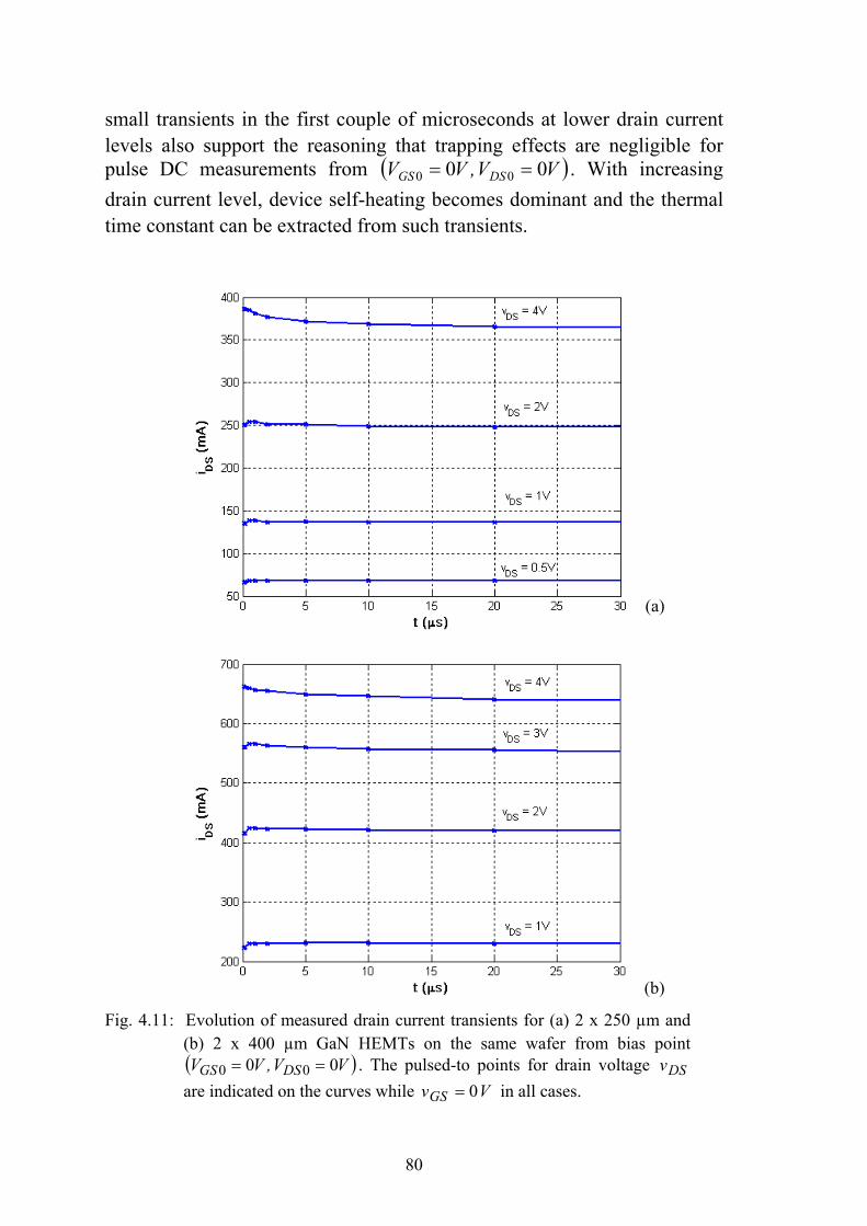
small transients in the first couple of microseconds at lower drain current levels also support the reasoning that trapping effects are negligible for pulse DC measurements from ( )VV,VV DSGS 00 00 == . With increasing drain current level, device self-heating becomes dominant and the thermal time constant can be extracted from such transients.
Fig. 4.11:
80
(a)
(b)
Evolution of measured drain current transients for (a) 2 x 250 µm and (b) 2 x 400 µm GaN HEMTs on the same wafer from bias point ( )VV,VV DSGS 00 00 == . The pulsed-to points for drain voltage DSv are indicated on the curves while VvGS 0= in all cases.

81
The drain current transient to the pulsed-to point ( )Vv,Vv DSGS 40 == in Fig. 4. 11(a) is shown separately in Fig. 4.12. This transient shows two different time constants; a fast initial fall and then followed by a slow decrease. This may be explained by an initial fast heat transfer to the epilayer causing a fast temperature increase, which is then followed by a slower temperature increase due to a thicker and better heat conducting SiC substrate. Although multiple time constants are required to fit the transient, a first order exponential curve fit gives a thermal time constant of 20.5 µs. A similar curve fit to the drain current transient of the 0.8 mm GaN HEMT [Fig. 4. 11(b)] gives a thermal time constant of about 30 µs.
Fig. 4.12: Measured drain current transients for 2 x 250 µm GaN HEMT from bias
( )VV,VV DSGS 00 00 == and pulsed-to point ( )Vv,Vv DSGS 40 == . Exponential curve fit (line) and data (stars). Inset: same drain current transient for 0 < t < 1 ms.
In order to obtain the trapping time constants, the thermal state of the device should remain unchanged at the quiescent bias and pulsed-to points. This may be accomplished by selecting these points along constant dissipated power curve [87]. Such drain current transient measurement results are shown in Fig. 4.13 for a 2 x 250 µm GaN HEMT. The dissipated DC power at the two quiescent bias points (-3.5V, 21V) and (-1V, 4V) is approximately the same, which is equal to 1.4W.

82
(a)
(b) Fig. 4.13: Measured drain current transients for 2 x 250 µm GaN HEMT from bias
points lying on constant power hyperbola. (a) Bias: (-3.5V, 21V), pulsed-to: (-1V, 4V). (b) Bias: (-1V, 4V), pulsed-to: (-3.5V, 21V).
The transient measurement from quiescent bias (-1V, 4V) to the pulsed-to point (-3.5V, 21V) gives a drain current that decreases to its steady value as charge trapping progresses. Conversely, pulsing in the opposite direction from the quiescent bias (-3.5V, 21V) to the pulsed-to point (-1V, 4V) results in de-trapping of charge and hence a gradual drain current increase to the steady state value. Again, simple exponential curve fitting to these

83
curves gives time constants of about 2 µs and 4.5 µs for Fig. 4.13(a) and Fig. 4.13(b), respectively.
However, these transient measurements require the alteration of both the gate and drain voltages from quiescent bias to the pulsed-to point in order to stay on the constant power curve. Hence, it is not possible to relate these time constants separately to the gate or drain voltages and thus to surface or buffer trapping. Therefore, this measurement technique is useful if either the gate lag or drain lag effect only is present. Nevertheless, the procedure gives gross estimate of the trap time constants.
4.4.3 Characterization of High Power HEMTs
The large-signal model of large power devices should be derived from measurement data directly instead of model scaling whenever possible. Measurement based models are more accurate as model scaling rules for large devices becomes more complicated due to nonlinear increase in self-heating. However, the device characterization techniques discussed in earlier sections become increasingly difficult with increasing size of power devices. The lower impedance levels and higher power dissipation in larger power FETs make the measurement tasks difficult.
Since the current densities of AlGaN/GaN HEMTs are in the order 1 A/mm, most of the commercially available pulsed I(V) systems can not fully characterize large gate-periphery devices in full voltage domain. As an example, Fig. 4.14(a) shows the pulsed I(V) measurement results for a 4 mm GaN HEMT in limited voltage ranges. The 2A maximum current rating of the pulsed I(V) analyzer used here does not allow to measure the maximum drain current, Imax, of the transistor.
As discussed earlier, for such high power devices, the S-parameters also have to be measured under pulsed bias conditions for a more accurate large-signal model derivation. In fact for AlGaN/GaN on Si substrates of relatively smaller size than AlGaN/GaN on SiC substrates or for other devices with poor thermal management, self-heating becomes considerable. The static DC characteristics for these devices are much reduced as compared to their pulsed I(V) characteristics [see Fig. 4.14(b)]. The large dissipated power and the large gate-periphery makes heat conduction inefficient thereby resulting in fast droop in their DC characteristics. Additionally, the devices may also not able to sustain CW
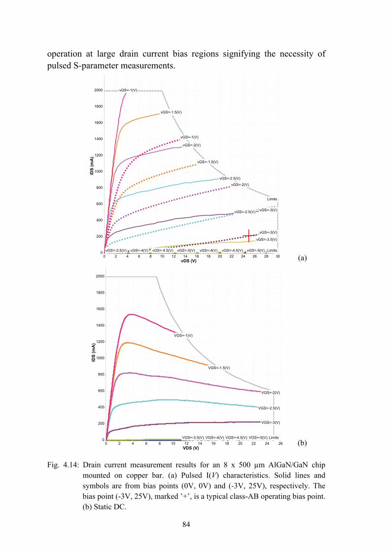
84
operation at large drain current bias regions signifying the necessity of pulsed S-parameter measurements.
(a)
(b)
Fig. 4.14: Drain current measurement results for an 8 x 500 µm AlGaN/GaN chip mounted on copper bar. (a) Pulsed I(V) characteristics. Solid lines and symbols are from bias points (0V, 0V) and (-3V, 25V), respectively. The bias point (-3V, 25V), marked ’+’, is a typical class-AB operating bias point. (b) Static DC.
0 2 4 6 8 10 12 14 16 18 20 22 24 26VDS (V)
0
200
400
600
800
1000
1200
1400
1600
1800
2000
IDS
(mA
)
LimitsVGS=-5(V)VGS=-4.5(V)VGS=-4(V)VGS=-3.5(V)
VGS=-3(V)
VGS=-2.5(V)
VGS=-2(V)
VGS=-1.5(V)
VGS=-1(V)
0 2 4 6 8 10 12 14 16 18 20 22 24 26 28 30vDS (V)
0
200
400
600
800
1000
1200
1400
1600
1800
2000iD
S (m
A)
LimitsvGS=-5(V)vGS=-4.5(V)vGS=-4(V)
vGS=-3.5(V)
vGS=-3(V)
vGS=-2.5(V)
vGS=-2(V)
vGS=-1.5(V)
vGS=-1(V)
Limits
vGS=-5(V)vGS=-4.5(V)vGS=-4(V)vGS=-3.5(V)
vGS=-3(V)
vGS=-2.5(V)
vGS=-2(V)
vGS=-1.5(V)
vGS=-1(V)

85
Chapter 5
Large-Signal Model of AlGaN/GaN HEMTs
In electrical equivalent circuit (EEC) based large-signal models of FETs, the drain-source, gate-source, gate-drain current functions, and charge sources (or nonlinear capacitances) represent the main nonlinearities of the devices. In general, these are functions of the instantaneous and average gate and drain terminal voltages and the channel temperature of the device. The derivatives of the charge sources model the displacement currents and the drain-source current models the channel conduction current.
In the conventional large-signal modeling procedure, both the charge, Q(V), and current, I(V), functions are obtained by integration of the bias dependent small-signal model elements [90]. In this technique, multi-bias S-parameter measurement data is the basis for the determination of the bias dependent small-signal model elements as discussed in Chapter 3.
The drain-source current generator is the dominant and the most important nonlinearity of a FET. Its accurate modeling is vital, among others, to faithfully represent the DC and dynamic I(V) characteristics of the device. The main problem in this regard has been to take into account the low-frequency dispersion phenomenon. Consequently, numerous attempts were directed to improve the model accuracy by developing dispersive nonlinear current models (e.g. [67], [88], [91]-[92]).
As was discussed in the previous chapter in some detail, the effects of low frequency dispersion are seen between statically and dynamically measured drain current characteristics. In terms of the small-signal equivalent circuit parameters, dispersion is observable in the transconductance and output conductance. In other words, these differential drain current parameters become low-frequency dependent.
86
In this chapter, the determination of the nonlinear charge model from multi-bias S-parameter data is discussed first. Next, the conventional drain current modeling techniques will be reviewed followed by an in depth discussion of the derivation of the drain and gate current models from pulsed DC measurements. The rest part of the chapter deals with model implementation and verification issues.
5.1 Nonlinear Charge Modeling
Nonlinear charge (or nonlinear capacitance) models were found to be important for the accurate prediction of the intermodulation distortion of a FET [93]. Several issues need to be considered to derive the nonlinear two-port charge models for FETs, which include identification of the nonlinear capacitances from measured data, transcapacitance(s), and terminal charge conservation.
The problem in the nonlinear charge model derivation stems if the integrability condition is not satisfied by the measured intrinsic admittance data as given by (4.14) due to dispersion effects. Additionally, transcapacitance(s) elements in the intrinsic FET circuit are necessary to fit the bias-dependence of these admittance data. The inclusion of the transcapacitance(s) elements is, therefore, also meant to conserve the integrability condition if it is satisfied by the measured admittance data. In other words, the transcapacitance, which is analogous to the term transconductance, is necessary to better fit the bias-dependence of the intrinsic admittance data and for the resulting derived large-signal model to be terminal charge conserving [94].
Hence, if the measured data is fulfilling the integrability condition and the intrinsic FET circuit small-signal model elements extracted include at least one transcapacitance, the charge models can be derived by path-independent integration [94]. Consequently, the resulting large-signal model will be consistent with the small-signal model thereby reproducing the measured bias-dependent small-signal parameters that were used to construct it.
In practice, the integrability condition is well satisfied over most of the voltage space except in the linear region [67] [77]. Consequently, the computed charge model becomes integration path dependent. The resulting

87
large-signal model may not be able to reproduce the small-signal measured data accurately and hence model inconsistency.
There were different approaches to solve the consistency problem between the nonlinear large-signal and the corresponding linear small-signal models. These include the top-down modeling technique discussed in Chapter 4, which is based on non-conventional equivalent circuit topology and modeling procedure. But there were also attempts to introduce transcapacitance elements to the conventional modeling techniques (e.g. [94]-[95]). However, some of these methods result in undetermined system as the introduction of these additional transcapacitance(s) result in increased number of intrinsic FET elements. Consequently, the commonly used analytical extraction procedures [46] for intrinsic FET model elements cannot be applied, and in that case the extraction procedure must resort to optimization techniques.
In a number of recent works, nonlinear capacitance based large-signal models were implemented directly instead of charge sources to avoid the problem of path dependent integration [96]-[97]. In nonlinear capacitance-based large-signal models, however, DC spectral components will be generated unless terminal charge conservation conditions given in (4.14) are satisfied [94]. In order to avoid this unphysical DC current flow in the implementation of these capacitance based large-signal models, DC blocking capacitors in a simple RC and RLC configuration were used [97]-[98].
However, the charge Q(V) function is generally less dispersive than the current I(V) function [33]. Therefore, conventional modeling methods can be used to derive the charge function Q(V). If thermal effects were to be considered for large sized power FETs, S-parameters are measured at different temperatures from which temperature, and bias-dependent intrinsic capacitances are extracted [96].
The topology of the large-signal model of the AlGaN/GaN considered here (see Fig. 5.7) retains the structure of the small-signal model derived in Chapter 3. Note that all the nonlinear intrinsic model elements are available as function of the intrinsic voltages as shown in Fig. 3.16. The gate-source and gate-drain charge sources in the large-signal model incorporate the effects of the three capacitances )V,(VC dsgsgs , )V,(VC dsgsgd and
)V,(VC dsgsds . These charge sources are obtained by integrating over the bias-dependent capacitances as follows [99],

88
∫∫ +=)V,V(
)V,V(dsds
)V,V(
)V,V(gsgsdsgsgs
dsgs
dsgs
dsgs
dsgs
dVCdVC)V,V(Q0000
(5.1)
( )∫∫ −−+=)V,V(
)V,V(dsdsgd
)V,V(
)V,V(gsgddsgsgd
dsgs
dsgs
dsgs
dsgs
dVCCdVC)V,V(Q0000
(5.2)
where )V,V( dsgs 00 is an arbitrary integration starting point.
5.2 Drain Current Models Based on DC I(V) and S-Parameters
Among the early techniques in developing dispersive drain current models, DC to HF transition is described by filter functions. The large-signal drain conduction current for a table-based large-signal FET models is expressed as [67],
( ) )V,V(I*)(H)V,V(I*)(H)(I DSGSHFDSDSGS
DCDSDS ωωω −+= 1 (5.3)
where )(ωH is a low-pass filter and DCDSI is obtained directly from DC
measurements. The state function HFDSI models the nonlinear drain current
above the cutoff frequencies of dispersion effects. It is usually computed from measured multi-bias S-parameter data.
The same basic technique is followed in other works (e.g. [92]) where an RC filter circuit is used with the high frequency component of the drain current source. The values of the R and C are estimated by comparing the measured and modeled low-frequency output impedances.
The basic problem with these approaches has been the characterization of the FETs on which the large-signal model is based. The modeling procedures rely on standard CW S-parameter measurements. These techniques may work well for low power FETs, as the self-heating effects are not significant. But the method is less suitable for the new III-V devices with large power density and not matured technology. For complete representation of the nonlinear large-signal model elements such as the drain-source current, they must be functions of instantaneous and average voltages as well as the channel temperature. These bias and temperature

89
dependence of the drain-source current has already been shown using pulsed DC characterization (see Fig. 4.9 and Fig. 4.10).
As discussed in the next section, the derivation of dispersive drain-source generator from CW S-parameter data is unsuitable for dispersive high power FETs. As one of the researchers in the field described it, large-signal model simulation and actual RF output power started to compare well after the use of pulsed DC measurements for I(V) model at the beginning of the 1990s [66]. Hence, most recent works are based on pulsed DC I(V) measurements. Additionally, time constants related to the different dispersion effects are required to model the transition between the DC and RF frequency.
5.3 Data Base for Dispersive Large-Signal Models
It is well known that some high power FETs do not deliver as much power at microwave frequencies as would be expected from their static I(V) characteristics. It is also true that conductances and transconductances calculated from curve tracers or parameter analyzer curves are different as compared to those obtained from S-parameter measurements performed at high frequencies [100]. In other words, the dynamic and static I(V) characteristics of a FET are different. The reason being the dispersion effects that have been discussed extensively in this thesis. But the relevant questions are which measurement(s) gives the RF current of the FET that represents a match to the RF loadline under high frequency operation? And how to represent these measurement data in the large-signal model of the FET?
These same questions may be raised for the charge, Q(V), functions of the large-signal model of a FET as well. But as discussed in the previous section, charge functions are assumed to be less dispersive and standard methods are used to derive their models in this thesis. However, for AlGaN/GaN HEMTs with larger gate-periphery, self-heating effects becomes substantial and hence pulsed S-parameter measurements are required to derive the charge functions.
It is useful at this point to review why large-signal modeling based on multi-bias standard CW S-parameter measurements would give incorrect I(V) model for high power devices. The multi-bias S-parameters measured are small-signal properties that are local to the bias points under

90
consideration. Since the response of the FET changes with the operational state (e.g. bias voltage and ambient temperature), it has different RF characteristics from a local (e.g. standard S-parameter) and from a remote (e.g. pulsed S-parameters) bias points.
To emphasize this point further, an example is considered that would compare the high frequency conductances obtained from two different bias states of a HEMT. A similar discussion is given in [33]. We compare measured conductances of the HEMT from two different bias points and for a given pair of instantaneous gate and drain voltages, ),( DSGS vv . The first case is when the bias point is remote from these instantaneous voltages and the second case is when the HEMT is actually biased at these same voltages. These two cases represent the conduction currents obtained from pulsed DC and S-parameter measurement systems, respectively.
Considering the first case where the GaN HEMT is biased at a remote point Q1 (marked +) in Fig. 5.1 for large-signal operation (e.g. as a class AB-amplifier). The pulsed I(V) characteristic from this bias point is shown by the marked curve. The drain current at any point on this curve is function of the state of the device at the bias point Q1 and the large gate and drain pulse voltages. This drain current may then be written as
( )00 ,,, i DSGSDSGSDS VVvvf= . Taking our specific example for the 0.5 mm GaN HEMT, ( )VVVVvVvf DSGSDSGSDS 30,5.3,,1 i 00 =−=−== .
As a class-AB amplifier and under some impedance and large input signal conditions, the dynamic drain current may swing to the point
)5,1( VvVv DSGS =−= , which lies on this curve. The conductance at the point )5 ,1( VvVv DSGS =−= can be calculated from the slope of the curve (shown
by dashed line).
Actually, the assertion that the loadline of the HEMT under RF operation follow the pulsed I(V) characteristics can be debated. But recent experimental results showed that the RF loadlines correlate with pulsed I(V) characteristics when the quiescent operating bias points of both pulse and RF operation are the same [83]. This was discussed in Chapter 4 (see Fig. 4.6).
Now consider the second case where the HEMT bias point has been moved to Q2 ( VVVV DSGS 5,1 00 =−= ). The conductance obtained from standard S-parameter measurements at this point is sought. If we make pulsed DC measurement having this quiescent bias point, the dynamic drain current function can be written as

91
( )VVVVvVvf DSGSDSGSDS 5,1,,1 i 00 =−=−== . The conductance calculated for infinitesimal variations of the drain voltage in the neighborhood of the bias point Q2 would be similar to the one obtained from standard S-parameter data at same bias point. The slope of the curve at point Q2 gives the conductance that would have been obtained from S-parameter measurement.
Fig. 5.1: Dynamic I(V) characteristics of a 2 x 250 µm GaN HEMT from two different quiescent bias points. Marked curve from Q1: )VV,V.V( DSGS 3053 00 =−= and solid curve from Q2: )VV,VV( DSGS 51 00 =−= . Both are for VvGS 1−= .
Obviously, the conductances from these two procedures are different. Hence showing incompatibility of S-parameter data and actual large-signal device behavior from a remote operating bias point. A similar analysis would also show that their transconductances and other higher order derivatives of the drain currents are different. But conductances, transconductances and other higher order derivatives of the drain current quantities, among others, are essential for correct prediction of the fundamental and harmonic output power, gain and gain compression.
0 5 10 15 20 25 30 35 400
20
60
100
140
180
220
260
300
340
vGS=-1(V)
Limits
vGS=-1(V)
i(m
A)D
S
v (V)DS
Q1

92
This comparison can be repeated for any other point thus revealing the unsuitability of the multi-bias S-parameter measurements to determine the large-signal model elements.
We may also need to note that the dynamic I(V) from bias point Q2 in Fig. 5.1 may lie below the dynamic I(V) measured from bias point Q1 for other devices with large self-heating effects (e.g. AlGaN/GaN HEMT on Si).
In the next sections, procedures are discussed that describe the derivation of I(V) functions of large-signal model from pulsed DC measurements. This applies for both the gate- and drain-source current models.
5.3.1 Drain Current Models Based on Pulsed I(V) Measurements
Pulsed DC FET characterizations were discussed at length in Chapter 4. It was shown that the I(V) characteristics are function of both the instantaneous and the average terminal voltages as well as the channel temperature of the FET. Therefore, the drain current functions of FETs in large-signal models based on the pulsed I(V) measurements need to represent these dependencies on the five variables.
The simplest and a quiescent bias point specific I(V) model can be derived by taking one set of pulsed DC measurement from the intended operating bas point of the device. The measured data can then be used directly in table-based models [101] or fitted to analytical function [102]. Since the measured pulsed drain current is taken at the intended operating bias point of the transistor, the large-signal model and actual device operation have the same trap and thermal state. Hence, the large-signal model is expected to be accurate assuming other nonlinearities are modeled properly. The problem is, of course, changing the operating bias point may require repeating the modeling process for the new quiescent bias point.
A more general I(V) model can be derived using sets of pulsed DC characteristics taken from different bias points [86] [88] [103]. The drain current function may be written as [88],
( )chDSGSDSGSDS T,V,V,v,vf i 00= (5.4)

93
where GSv and DSv are the instantaneous voltages applied to the device ports. 0GSV and 0DSV are DC components which are dependent on the quiescent bias voltages and the mean values of gate and drain terminal voltages. The average channel temperature chT models the influence of thermal effects.
The determination of the I(V) model parameters described by (5.4) from pulsed DC measurements need to identify the drain current dependence on the terminal voltages and the channel temperature. One needs to define the functional form of the drain current and identify its parameters from measurement data. The function must be able to describe the observed drain current dependence on instantaneous and average voltages and as well as channel temperature. Procedures must also be developed for the required measurement data and the sequential identification of the model parameters. Two common methods are discussed below.
One technique, described in works of Jastrzebski et al. [103], models the drain current by taking the pulsed I(V) characteristics from quiescent bias ( VVVV DSGS 0,0 00 == ) as a reference. For a given pulsed-to voltage point ( DSGS vv , ), the pulsed DC drain currents from this bias point are larger than pulsed DC drain currents from any other bias point. This I(V) characteristics may be taken as dispersion free which means that it is free of current collapse and it has minimum knee voltages. Consequently, the I(V) characteristics represents the greatest potential of the device under RF operation.
The trap and thermal effects are then modeled by functions that modify this reference current in multiplicative way. The drain current, as function of the instantaneous terminal voltages GSv and DSv and also the mean values of these voltages ( 0GSV and 0DSV ), is written in [86] [103] as
( ) thermaltrapDSDSGSDSGSDS ffi V,V ,v ,v i ××= 000 (5.5)
where ( )DSGSDS fi v,v0 = is the reference current just described which is function of the instantaneous terminal voltages only. The traps due to varying drain bias voltages can be accounted by ( )DSGSDStrapD Vff v,v,0= . This model parameter can be identified by taking pulsed-DC measurements with varying drain bias voltages but at a fixed gate bias voltage. A similar function, ( )DSGSGStrapG Vff v,v,0= , could also be used to model traps due to gate bias variations whereby pulsed-DC measurements are taken with

94
varying gate bias voltages but at a fixed drain bias voltage. The channel current variation due to internal power dissipation, dissP , is modeled by
( )dissthermal Pff = .
It may be understood that large pulsed DC datasets are required to determine trapDf and trapGf to establish their corresponding bias voltages dependence. A series of measurements need to be taken along constant gate and constant drain bias conditions that exclude self-heating effects. In [86], for example, 31-pulsed I(V) data sets are used to identify trapDf alone. As per this publication, similar number of measurements are required to determine the parameters trapGf and thermalf .
The technique that will be discussed next requires much less number of pulsed DC measurements. This method has been adopted in this thesis for AlGaN/GaN HEMTs. It is based on the approximation that (5.4) can be linearized with respect to the bias voltages, 0GSV and 0DSV , and the channel temperature, chT . The linearization of (5.4) in the neighborhood of a nominal operating point *
0GSV and *0DSV and a channel temperature *
chT gives [88]
( ) ( )[ ][ ]
( ) ( )[ ]**00
0
0
00
PP) v,(vf
) v,(vf) v,(vf
,,V,V , v,vi
ccthDSGS
DSDSDSGSD
GSGSDSGSG
DSGSISODSchDSGSDSGSDS
TTR
VvVv
vviT
−+−+
−+−+
=
θ
(5.6)
where ( )DSGSISODS vvi , is an ideal equi-thermal DC characteristic
corresponding to a constant channel temperature *chT . The functions
*0GSG Vff ∂∂−= and *0DSD Vff ∂∂−= model the deviation between the static and dynamic drain current due to traps. The function Gf accounts for traps associated with surface state, which is primarily function of the gate quiescent bias voltage. Similarly, Df models trapping phenomena at the channel-substrate interface which is mainly function of the drain bias.
Concerning thermal effects, the function *chTff ∂∂=θ accounts for the device heating or cooling due to self-heating and/or case temperature ( cT ) variations. The change in the channel temperature due to self-heating effect is the product of the average dissipated power, ,P0 and the thermal

95
resistance of the device structure, ,Rth [ )PP(R *th 00 − ] and/or change in
case temperature [ *cc TT − ]. The thermal resistance of the device structure,
,thR represents the total thermal resistance between channel and case (or chuck for a device on wafer). It may be determined in one of two ways as discussed in section 5.3.3.
The identification of the four model parameters ( )DSGSISODS vvi , ,
( )DSGSG vvf , , ( )DSGSD vvf , and ( )DSGS vvf ,θ requires a minimum of four pulsed DC datasets taken from different quiescent bias and/or ambient temperature conditions of the FET. These four model parameters can then be determined by solving simultaneously four linear equations corresponding to each of the bias voltage. The I(V) model may be obtained for constant or varying case temperatures [88].
If the model parameters are to be identified for a fixed case temperature then an explicit knowledge of the thermal resistance of the device structure is not necessary. In this case the thermal effect is due to the self-heating only and the function ( ) ( ) thDSGSDSGSP Rvvfvvf ⋅= ,, θ can be used instead.
The other case is when the model is to be valid as function of different case temperatures. In that case, a priori knowledge of the thermal resistance of the device structure or pulsed DC data as function different case temperatures is required.
In all cases, however, the choice of the quiescent bias conditions should be done with careful consideration. Specially, the pulsed DC measurement should be taken from quiescent bias points where trapping effects are significant in order to determine parameters Gf and Df with better accuracy. Quiescent bias points that would result in ill-conditioned linear equations should be avoided. This can be done, for example, by choosing the bias points at low and high voltage ranges as discussed in section 4.4.1.
The application of this technique to 1 mm GaN HEMT, whose pulsed DC characteristics are shown in Fig. 4.9 and Fig. 4.10 results in the extracted model parameters shown in Fig. 5.2. The functions show a smooth curve and a clear transition from pinch-off region to active regions. All the three functions Gf , Df and θf are zero in pinch-off region and for zero drain voltages as expected. The function Df picks up near knee voltages but decreases for higher drain voltage values, which can be understood if one makes a closer look at the pulsed I(V) dataset in Fig. 4.9(b). A strong decrease in measured pulsed DC drain current, as

96
compared to say the drain current from quiescent bias ( VVVV DSGS 0,0 00 == ), is observed when the “pulsed-to” drain voltages are less than the quiescent bias (i.e. for 0DSDS Vv < ). But the decrease is smaller for “pulsed-to” drain voltages greater than the quiescent bias,
0DSDS Vv > . In other words, negative and positive drain voltage pulses relative to the quiescent bias voltage result in different trapping effects. A more pronounced asymmetry in the trapping process has been observed in SiC MESFETs [87]. The shape of θf also follows the usual trend of self-heating of a FET due to dissipated power which increases with drain current and voltage.
(a)
(b)

97
(c)
(d)
Fig. 5.2: Dispersive drain current model parameters based on techniques described in [88]. (a) Isothermal current, ( )DSGS
ISODS v,vi and functions modeling traps and
thermal effects (b) ( )DSGSD v,vf (c) ( )DSGSG v,vf and (d) ( )DSGS v,vfθ .
These drain current model parameters were then interpolated for denser grid and extrapolated for greater voltage ranges than those shown in Fig. 5.2. This is important before the lookup table implementation of the model parameters in a nonlinear simulator. The data processing helps to avoid interpolation and unphysical extrapolation problems, unphysical simulation results and to avoid CAD simulation convergence problems. A processed sample data of the isothermal drain current model parameter of Fig. 5.2(a) is shown in Fig. 5.3.

98
Fig. 5.3: The isothermal current, ( )DSGSISODS v,vi , shown in Fig. 5.2(a) interpolated for
denser grid voltages and extrapolated to larger voltage ranges.
5.3.2 Diode Current Models
The output power of a typical FET is limited by a gate-forward conduction and reverse gate-to-drain breakdown. These can easily be understood by considering a typical I(V) characteristic of a FET under large-signal conditions [40]. Depending on the bias point of the FET and the RF input power level, the device can be driven into gate-forward conduction and/or a gate-to-drain breakdown. If an RF loadline for maximum output power is considered, the output current and voltage swings are from maximum channel current to pinchoff and from knee voltage to some high voltage, respectively. At the left-hand corner of the RF loadline, the RF output current waveform is clipped by gate forward conduction and channel current saturation. At the other end of the loadline, large positive drain voltage and negative gate voltage lead to gate-to-drain breakdown currents thereby limiting the output voltage available.
Generally, there is difference between the static and dynamic gate currents. The dynamic gate current obtained from pulsed DC measurement is function of the quiescent bias voltages and the instantaneous voltages in a similar way as the drain current. Consequently the gate-forward current

in the large-signal model of the HEMT is also based on pulsed DC measurements for the following reasons. First, the quality of measured data and safety of the power devices is better insured with the pulsed DC measurement set up. More importantly, the dynamic response of the device under RF excitations matches to the pulsed DC characteristics better than to the static DC. Earlier research work on gate-to-drain breakdown current has also shown that accuracy of the large-signal model simulation improves for a MESFET when based on pulsed DC data [104].
Measurements of the gate-forward current for different size AlGaN/GaN HEMTs on SiC substrates have shown that it is a function of both gate- and drain-voltages. This demonstrates that the usual diode equation model of a Schottky contact cannot be used. Such a model would be correct for constant zero drain voltage which applies only if the source and drain terminals are connected together. As this is not the normal operation of a FET, the gate-forward current must be modeled to reflect this gate and drain voltage dependence.
Fig. 5.4: (V
A typia 0.5 mmincreasing
16
99
Pulsed DC gate-forward current of a 0.5 mm GaN HEMT. Measured symbols) and large-signal model simulation (lines). Bias:
VV,V DSGS 00 00 == . vGS = 1.6V (top) with 0.1V step.
cal pulsed DC gate-forward current, ,iGS is shown in Fig. 5.4 for AlGaN/GaN HEMT. The gate-forward current decreases with drain voltage. Similar characteristics have also been reported for
0.5 1.0 1.50.0 2.0
2
4
6
8
10
12
14
0
vDS (V)
iGS
(m
A)

100
GaAs FETs [33]. The form of GSi as function of drain voltage depends upon the device structure, particularly the channel doping and thickness and the gate length [33]. The measurement of such pulsed DC gate current also requires great care as the current increases exponentially with gate voltage for zero drain voltage.
The gate-forward current should, therefore, be represented in the large-signal model of the FET by a current generator that is function of both gate and drain voltages. An analytical function of two variables may be fitted to these data. Here, a table-based data is used directly for its implementation in ADS®. This is a similar model implementation as the drain current model. The results of model simulation and measurement are compared in Fig. 5.4. This will improve the large-signal model simulation for RF input power levels that drive the device into gate-forward regions.
5.3.3 Thermal Modeling of AlGaN/GaN HEMT Structures
Since the current density in AlGaN/GaN HEMTs is about 1 A/mm, self-heating is a serious problem affecting the device’s performance and reliability. In this respect, AlGaN/GaN HEMTs on SiC substrates are better as compared to those on Si or sapphire substrates. SiC is an excellent thermal conductor and heat convection from the HEMT to the ambient is relatively more efficient. Consequently, the influence of self-heating on device characteristics is not dramatic for small gate-periphery HEMTs. In contrast, AlGaN/GaN HEMTs on Si or sapphire substrates have static DC characteristics greatly different from their pulsed DC I-V due to their higher channel temperature.
In any case, accurate estimation of the channel temperature of a high power HEMT is one of the most important steps in the large-signal model development procedure. Specially, self-heating in large gate-periphery power FETs is more pronounced than in small size FETs. For large size multi-finger FET, heat diffusion from active area of the transistor to the ambient is less efficient due to multiple neighboring heat sources. In fact, due to non-uniform lateral heat diffusion in such devices, the center-fingers are at higher temperature than the edge fingers [105].
In theory, the steady-state channel temperature due to self-heating effects may be obtained by solving heat flow equation. The temperature at

101
any position in the device structure may be obtained by solving the heat flow equation [106],
[ ] Pz)y,(x,Tκ(T) −=∇⋅∇ (5.7)
where T is the temperature in Kelvin and P is the dissipated power density in W/m3. κ(T) is a temperature dependent thermal conductivity of a given layer in W/m·K. It decreases with increasing temperature for the materials under consideration (see Fig. 5.5).
Typically, the layered structure of an AlGaN/GaN HEMT from the channel to the base includes the buffer (GaN), nucleation (GaN, AlN or AlGaN), substrate (SiC, Si or sapphire) and a heat sink (see Fig. 2.1(a)). The AlGaN/GaN HEMTs treated here are on semi-insulating 4H-SiC substrates [31]. Hence we need to consider the thermal conductivities of GaN and SiC materials. These are given by [107]
b
000 κ κ(T)
−
⎟⎟⎠
⎞⎜⎜⎝
⎛⋅=
TT (5.8)
where 00κ is the thermal conductivity at room temperature )300( 0 KT = .
KcmW⋅
= 6.100κ and 4.1=b for GaN. Kcm
W⋅
= 3.300κ and 5.1=b for
SiC.
The thermal conductivity being function of temperature makes the heat equation in (5.7) nonlinear thereby making the calculation of the solution tedious [108]. However, Kirchhoff’s transformation converts the nonlinear equation to a linear one, with linear boundary condition, for any functional form of the temperature dependent thermal conductivity, κ(T), [108]. Therefore, this method has been widely used in thermal modeling of semiconductor devices through analytical techniques.
Nevertheless, the steady-state thermal analysis of layered (inhomogeneous) structure, each with different temperature-dependent thermal conductivity, is a problem. The main difficulty is, unless the ratios of the heat conductivities of adjacent layers are temperature independent, the transformed temperatures across the boundary separating the homogenous regions will be discontinuous [106]. Obviously, the ratio of

102
)()( TT SiCGaN κκ for the GaN HEMT on SiC structure is function of temperature and hence the resulting temperature solution is discontinuous at the boundary of GaN buffer and SiC substrate.
Fig. 5.5: Thermal conductivity,κ(T), for GaN epitaxial layers and SiC substrates of
GaN HEMT given by (5.8).
However, for the practical HEMT structures, the GaN epilayer is very thin (a few micrometers) as compared to the thickness of the substrate (see Fig. 2.2). Consequently, the substrate material primarily determines the thermal impedance of the HEMT structure [109]. Hence the temperature dependence of the thermal conductivity of SiC substrate only can be considered.
A simplified approach is, therefore, to estimate the channel temperature of a device by assuming first a constant thermal conductivity [96]. In order to estimate the channel temperature, e
chT , at a given bias point, a linear relationship between average dissipated power and temperature is assumed,
00 TPRT dissthe
ch += (5.9)
where C/W)(R th ° is the thermal resistance of the device structure and 0T is the ambient temperature. The average dissipated power in the HEMT is
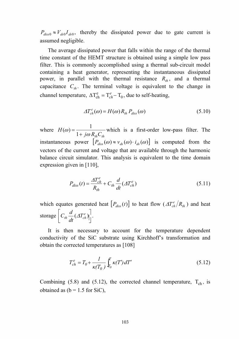
103
,000 dsdsdiss IVP ≈ thereby the dissipated power due to gate current is assumed negligible.
The average dissipated power that falls within the range of the thermal time constant of the HEMT structure is obtained using a simple low pass filter. This is commonly accomplished using a thermal sub-circuit model containing a heat generator, representing the instantaneous dissipated power, in parallel with the thermal resistance thR , and a thermal capacitance thC . The terminal voltage is equivalent to the change in channel temperature, 0
ech TT∆T −= e
ch , due to self-heating,
)()()( ωωω∆ dissthe
ch PRHT = (5.10)
where ththCRj
Hω
ω+
=1
1)( which is a first-order low-pass filter. The
instantaneous power [ ])()()( ωωω dsdsdiss ivP ⋅≈ is computed from the vectors of the current and voltage that are available through the harmonic balance circuit simulator. This analysis is equivalent to the time domain expression given in [110],
)()( echth
th
ech
diss TdtdC
RTtP ∆∆
+= (5.11)
which equates generated heat [ ])(tPdiss to heat flow ( the
ch RT∆ ) and heat
storage ⎥⎦⎤
⎢⎣⎡ )( e
chth TdtdC ∆ .
It is then necessary to account for the temperature dependent conductivity of the SiC substrate using Kirchhoff’s transformation and obtain the corrected temperatures as [108]
Td)Tκ()κ(T
1TTT
T0
0e
ch0
′′+= ∫ (5.12)
Combining (5.8) and (5.12), the corrected channel temperature, chT , is obtained as (b = 1.5 for SiC),

104
b−
⎟⎟⎠
⎞⎜⎜⎝
⎛ +=
11
b0
0ech
ch T)T b b)T-(1 T (5.13)
In the implemented large-signal model (see Fig. 5.7), this channel temperature is iteratively computed during the model simulation process. For a given drain current computed by (5.6), chT is calculated using (5.10) and (5.13) which is then used to get a new drain current and so on until the procedure converges.
The next section discusses the determination of the thermal resistance of the HEMT structure required in (5.10) to compute estimated channel temperature, e
chT .
5.3.3.1 Thermal Resistance
One possibility to estimate the thermal resistance of a FET structure is based on analytical expressions [111]. The method defines two regions for an AlGaN/GaN HEMT structure as shown in Fig. 5.6 and derived the following expression for the total (i.e. epitaxial layers and substrate) thermal resistance of the FET.
⎟⎟⎟⎟⎟⎟
⎠
⎞
⎜⎜⎜⎜⎜⎜
⎝
⎛
⎟⎟⎠
⎞⎜⎜⎝
⎛⎟⎠⎞
⎜⎝⎛−⎟
⎠⎞
⎜⎝⎛
⎟⎟
⎠
⎞
⎜⎜
⎝
⎛⎟⎟⎠
⎞⎜⎜⎝
⎛−⎟⎟
⎠
⎞⎜⎜⎝
⎛
+
⎟⎟⎟⎟⎟⎟
⎠
⎞
⎜⎜⎜⎜⎜⎜
⎝
⎛
⎟⎟
⎠
⎞
⎜⎜
⎝
⎛⎟⎠⎞
⎜⎝⎛−⎟
⎠⎞
⎜⎝⎛+
⎟⎟⎠
⎞⎜⎜⎝
⎛
+
⎟⎟⎠
⎞⎜⎜⎝
⎛=
21
2
2
2
12
2
21
21
1
24
2
41
221
21
41
st
sWh
tt
tWh
lnsk
st
sWf
tWf
lnkW
Ltln
kWR
G
G
SiC
G
G
SiCG
GGaNGtotal
ρ
πρ
π
π
ρ
ρπ
ππ
(5.14)

where the geometrical dimensions t1, t2, s, LG, and WG, are as shown in Fig. 5.6. The definition of the parameter ρ and the functions )(f ⋅ and )(h ⋅ can be found in [111]. kGaN and kSiC are the thermal conductivities of the GaN epitaxial layers and the SiC substrate at room temperature (see Fig. 5.5).
The dimensions assumed for the 8 x 125 µm GaN HEMT on SiC substrate are listed in Table 5.1 for determination of Rth using (5.14). The geometric parameters are usually not easy to get, as they are highly proprietary to the foundries. In any case, this method results in a calculated thermal resistance of thR = 13.68 °C/W. Note that this is the thermal resistance for total gate width of the HEMT whereas the analytical equation in (5.14) is for a unit gate width (i.e. N/RR totalth = ). Obviously, the dissipated power per unit gate width should be considered to calculate the temperature increase using (5.10) if totalR instead of thR is used.
Fig. 5.6: GaN
desiGaNand
Table 5.1: H
LG [µm] W
0.5 1
* Based on
105
HEMT structure and dimensions for Rtotal calculation (after [111]). The gnated dimensions are: surface area of heat source under gate LG x WG, thickness t1, substrate thickness t2, gate-to-gate spacing (gate pitch) s, number of fingers N.
Dimensions and calculated thermal resistance for an 8 x 125 µm GaN EMT.
G [µm] s [µm] N tGaN [µm] tSiC [µm] Rth [°C/W]
Rth*
[°C/W] 25 50 8 2.8 380 13.68 12.06
reference [112], which is considers the SiC substrate only.
G
G
G
S
S
DGaN
SiCSubstrate
t1
t2
z

106
This closed form expression is a better alternative to numerical methods, which are not suitable for practical use. It is also claimed that the method is accurate within 1% - 2% of the numerical methods. However, the technique is not valid for all kinds of FET layouts. For example, the AlGaN/GaN HEMTs are assumed to have at least two fingers on both sides of the center finger in order to justify an adiabatic boundary condition in lateral direction assumed in deriving the analytical expression. Hence, the expression may not be accurate for two-gate finger HEMTs.
The other option to determine the thermal resistance of a FET is based on the dispersive drain current model discussed in previous sections and static DC measurement data. Once the I(V) model has been developed and implemented in nonlinear simulator, it can be used to simulate the static DC characteristics. Under static DC conditions, the contributions of Gf and
Df in (5.6) are zero and the static DC drain current DCDSDS I)t(i = reduces
to [88],
( ) ( )[ ]*cc
*thDSGS
DSGSISODS
DCDS
TTPPR)V,V(f
)V,V(I I
−+−+
=
0000
00
θ
(5.15)
Here, the only unknown parameter is the thermal resistance, which can then be iteratively optimized by comparing measured and simulated DC characteristics. The application of this technique to a 2 x 250 µm GaN HEMT gives thR = 16.5 °C/W. This method is a good alternative to the analytical function discussed above, as the latter is valid only for FETs with large number gate fingers. Moreover, the scarce device geometric data is not necessary when using this second option. In fact, the calculated thermal resistance using (5.14) is thR = 35 °C/W, which is clearly overestimated for this two gate finger HEMT. For FETs with only two gate fingers, there is considerable lateral heat diffusion. Hence, the transistor operates cooler (i.e. low thermal resistance) than HEMTs with larger number of gate fingers for the same dissipated power density per unit gate width.
The thermal modeling of the transistor is now complete with determination of the thermal resistance as described here and the measured thermal time constant presented in Chapter 4. The thermal capacitance is calculated from ththth CR=τ and the simple thermal sub-circuit (see Fig. 5.7) can easily be integrated within the large-signal model in the nonlinear circuit simulator.

107
5.4 Large-Signal Model Equivalent Circuit
The techniques for deriving the most important nonlinearities of a large-signal model of a FET were covered in the proceeding sections and in the previous chapters. It is now possible to describe the complete large-signal model of the AlGaN/GaN HEMT.
The topology of the large-signal model, including the parasitic elements, is shown in Fig. 5.7. This is essentially based on the structure of the multi-bias small-signal equivalent circuit discussed in Chapter 3. The symmetric intrinsic large-signal model topology contains two charge sources in series with their corresponding charging resistances for the gate-source and gate-drain branches. It also includes the gate-source and gate-drain diode models as well as the dispersive drain-source current.
Fig. 5.7: Large-signal GaN HEMT model including a thermal sub-circuit.
The thermal sub-circuit shown here is based on the description presented in the previous two sections. The estimated channel temperature increase obtained from this sub-circuit corresponds to the one calculated using (5.10). Note also that (5.13) has also been integrated in the model

108
implementation that corrects the estimated channel temperature obtained from this thermal sub-circuit. The corrected temperature is then used to find a new value of the drain current which in turn is used to estimate the dissipated power and so on. The simulator at run-time accomplishes this iterative procedure.
5.4.1 Model Implementation
The large-signal model in Fig. 5.7 has been implemented in Agilent’s Advanced Design System, ADS®. The single valued extrinsic parameters are represented by lumped passive elements whereas the nonlinear intrinsic model values are read from a look-up table. These nonlinear model parameters as function of an orthogonal set of gate and drain intrinsic voltages are made available in one of standard file formats.
The nonlinear model implementation is based on Symbolically Defined Devices (SDD) feature in ADS®. The SDD is an equation-based component that enables us to define nonlinear components without the use of source codes. Arbitrary relationships between any of its port voltages, port currents and their derivatives can be defined. A 12-port SDD shown in Fig. 5.8 is used to implement the intrinsic HEMT (inside the marked box) shown in Fig. 5.7. It is straightforward to compare the intrinsic HEMT in Fig. 5.7 with the port assignments in Fig. 5.8. Port 1 through 7 correspond to gsQ , gdQ , iR , gdR , dsI , gdI and ,I gs respectively. The remaining 5 ports are for auxiliary purpose only. Port 8 and 9 are used to evaluate the high frequency components of the gate and drain voltage, )Vv( GSGS 0− and )Vv( DSDS 0− in (5.6). The RC circuits on the gate ( STST CR ) and drain ( DLTDLT CR ) side define the charge trap time constants. These time constants are estimated from pulsed DC transient measurements as discussed in Chapter 4. Large resistance and small capacitance values are chosen in order to make the effect of the RC circuits on the large-signal model negligible. The transconductance time delay is modeled with a delayed gate voltage at port 10. The instantaneous power is calculated at port 11 and its average value at port 12. The voltage at port 12 is equivalent to the estimated channel temperature change. This should then be used to calculate the corrected temperature using (5.13). Note that port 11 is terminated with 1Ω resistor thereby making the port voltage ( 11V ) numerically equivalent to the instantaneous dissipated power. Similarly,
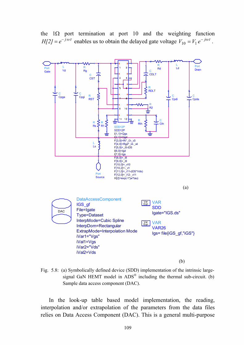
the 1Ω port termination at port 10 and the weighting function τωjeH[2] −= enables us to obtain the delayed gate voltage τjωeVV −= 110 .
(a)
Fig.
intereli
PortSource
LLs
RRs
RRST
CCST
PortDrain
CCpda
LLd
CCpdi
RRdPort
Gate
CCpga
LLg
CCpgi
RRg
RR1
RRDLT
CCDLT
RR2
SDD12PSDD12P
H[2]=exp(-1*jw*tau)F[12,0]=_i12-_v11F[11,0]=_i11-(iDS*Vds)F[10,2]=-_v1F[10,0]=_v10F[9,0]=_i9F[8,0]=_i8I[7,0]=IgsI[6,0]=IgdF[5,0]=_i5-iDSF[4,0]=Rgd*_i4-_v4F[3,0]=Ri*_i3-_v3I[2,1]=QgdI[1,1]=Qgs
CCth
RRth
VAREqnVar
DataAccessComponent
109
(b)
5.8: (a) Symbolically defined device (SDD) implementation of the intrinsic large-signal GaN HEMT model in ADS® including the thermal sub-circuit. (b) Sample data access component (DAC).
In the look-up table based model implementation, the reading, rpolation and/or extrapolation of the parameters from the data files es on Data Access Component (DAC). This is a general multi-purpose
VARVAR26Igs= fileiGS_gf,"iGS"
EqnVar
SDDIgate="IGS.ds"
IGS_gf
iVal2=VdsiVar2="Vds"iVal1=VgsiVar1="Vgs"ExtrapMode=Interpolation ModeInterpDom=RectangularInterpMode=Cubic SplineType=DatasetFile=IgateDAC

110
file reader in ADS®. A sample DAC for reading the gate current (see Fig. 5.4) from a file as function of the intrinsic gate and drain voltages is shown in Fig. 5.8(b). The file name containing the nonlinear parameter data, the dependent variable (the nonlinear parameter), the independent variables
gsV( and )Vds and their values, the interpolation and extrapolation modes have to be specified. Similar DACs are employed to read the other large-signal model parameters from the look-up table in a file.
However, one limitation of the DAC in the current ADS® versions is that the interpolation and extrapolation modes cannot be specified differently (e.g. spline interpolation and linear extrapolation). It is known that spline-interpolations are accurate within measurement region but may not extrapolate in a realistic way [68]. Hence simulation results at high power levels may be unphysical for large-signal model implementation of table-based models where processed measurement data is for limited voltage ranges.
5.4.2 Model Verification
Large-signal model verification is one of the last and important steps in modeling process. The model verification should, generally, include small-signal as well as large-signal power levels and under different bias conditions. The large-signal model test may include single-tone and two-tone (or complex modulated signal such as WCDMA).
The number and type of large-signal model tests depends on the purpose of the model developed for. As mentioned in Chapter 1, a large-signal model for a linear power amplifier design should obviously be validated for intermodulation distortion, which includes model simulation convergence and accuracy.
As in all other cases, large-signal measurements with single-tone, two-tone or modulated signal excitations should be carried with a well thought setup. The impedance environment to the device must be clearly known not only at the fundamental but also at harmonics and baseband frequencies. The same impedances at their corresponding frequency bands can then be presented to the large-signal model in the simulation process.
The large-signal models developed in this research work have been checked for accuracy and convergence under different input excitations

111
including single tone, multi-tone and transient simulations as detailed in the following sections.
5.4.2.1 Static and Pulsed I(V) Characteristics
The I(V) characteristics of FET are important in both the modeling process and during model validation. They represent the major nonlinearity of a FET and should therefore be tested. Since the large-signal model is based on pulsed DC I(V) characteristics which is implemented in a look-up table, the pulsed DC simulations for the datasets used in the modeling process are expected to be accurate. Therefore, model validation for the pulsed DC I(V) characteristics should be using different measurement datasets.
The static DC and pulsed DC simulations and the corresponding measured characteristics are compared in Fig. 5.9. Both the static and pulsed DC simulated characteristics compare well with measurement. The static DC test verifies the accuracy of the thermal resistance and the necessary temperature correction applied as per (5.13). The simulated channel temperature increase ( chT∆ ) corresponding to the static DC simulation is shown in Fig. 5.9(b). For each DC bias point, the corrected channel temperature increase ( chT∆ ) for the temperature dependent thermal conductivity of the substrate shows significant increase over estimated temperature ( e
chT∆ ) at high power levels, as expected.
The comparison of the pulsed DC simulation and measurement data from a class-AB bias point of (-3V, 30V) is a test for dispersive large-signal model. The bias dependent self-heating and trap effects have been modeled well and this is reflected in the agreement of the model and measurement under this exemplary bias condition. Note that the pulsed DC gate current model and its verification for a 0.5 mm AlGaN/GaN HEMT was presented in Fig. 5.4.

112
(a)
(b)
(c)
Fig. 5.9: Simulation (lines) and measured data comparison for a 2 x 250 µm GaN HEMT: (a) static DC and (c) pulsed DC from quiescent bias point (-3V, 30V). Channel temperature increase with bias points is shown in (b) where estimated dissth
ech PRT =∆ (cross) and chT∆ (lines) given by equation (5.13).
VGS = +1V (top), 0.5V step in (a) and (c).
4 8 12 16 20 24 280 32
50
100
150
200
250
300
350
400
0
450
VDS (V)
iD
S (
mA
)
5 10 15 20 25 30 35 40 45 50 550 60
50
100
150
200
250
300
350
400
0
450
vDS (V)
iDS
(m
A)
4 8 12 16 20 24 28 320 36
50
100
150
0
200
VDS (V)
VGS = 1V
∆Tch
and∆
T (
C)
e cho
∆T ech
0V
-1V
-2V
-3V
∆T ch

113
5.4.2.2 S-Parameters
Sample S-parameter simulations of the dispersive large-signal model as compared to measured data for active and pinch-off bias points are shown in Fig. 5.10. In general, the large-signal model has reproduced the small-signal behavior of the device quite good. Specifically, the small-signal gain ( 21S ) and the kink effect [113] in 22S are well predicted.
Noting here that the large-signal model derivation is based on CW S-parameters and pulsed I(V) measurements, the S-parameters simulation and measurement comparison will not be as good as the small-signal model verification shown Fig. 3.17. The different measurement conditions in the pulsed I(V) and S-parameter measurements (e.g. probe tip positions) are manifested in the small discrepancy between the measured data and simulation. This is, for example, seen in a small phase shift of 22S between measurement and simulation.
(a) (b)
Fig. 5.10: Large-signal model S-parameter verification of 8 x 125 µm GaN HEMT. The bias points (a) (VGS = -1.5V, VDS = 15V) is in saturation and (b) (VGS = -5V, VDS = 15V) in pinchoff region.
5.4.2.3 Large-Signal Waveforms
On wafer large-signal waveform measurements [114] enables us to get the large-signal response of the device directly at its gate and drain terminals.
5xS12
freq (0.5 to 20 GHz)
S11
0.05xS21
S22
S12
freq (0.5 to 20 GHz)
S11
-S21
-S22

114
This makes it possible for direct model verification at the device level instead of widely used indirect verifications using circuit designs (e. g. a power amplifier). This is an advantage since for the indirect method, the additional network making up the circuit (e.g. matching network) around the device complicates the model validation procedure.
The results in Fig. 5.11(a) show simulation and measurement results for two input power levels of a 1 mm AlGaN/GaN HEMT. The developed dispersive large-signal model simulation compares with measurement even for drive levels well into compression. There is a slight discrepancy when device is driven into gate-forward conditions (low drain voltage and high current regions) due to the gate diode current model. For this particular large-signal model, the usual diode current equation of a Schottky contact is used instead of the one described in section 5.3.2, due to lack of pulsed gate current measurement data similar to the one shown in Fig. 5.4.
Fig. 5.11: Large-signal measurement (circles) = 10 dBm and 22 dBm. C
GHzf,VVDS 215 == . (a) Drain showing extrapolation inaccuracy HEMT in 50Ω environment.
0.2 0.4 0.6 0.80.0 1.0
5
10
15
20
25
0
30
5
10
15
20
25
0
30
Time, nsec
VD
S [
V]
0.2 0.4 0.6 0.80.0 1.0
5
10
15
20
25
0
30
5
10
15
20
25
0
30
Time, nsec
VD
S [
V]
(a)
0.2 0.4 0.0.0
5
10
15
20
25
0
30
Time, nsec
VD
S [V
]
0.2 0.4 0.0.0
5
10
15
20
25
0
30
Time, nsec
VD
S [V
]
0.60.6
and simulation (lines) waveforms for Pin lass-AB bias: VGS = -3.2V and
voltage and current. (b) As in (a) but (see text). Device: 8 x 125 µm GaN
6 0.8 1.0
5
10
15
20
25
0
30
6 0.8 1.0
5
10
15
20
25
0
30
(b)
Time, nsec
IDS
[A]
0.2 0.4 0.6 0.8 1.0 1.2 1.4 1.6 1.80.0 2.0
0.1
0.2
0.3
0.4
0.5
0.0
Time, nsec
IDS
[A]
0.2 0.4 0.6 0.8 1.0 1.2 1.4 1.6 1.80.0 2.0
0.1
0.2
0.3
0.4
0.5
0.0

115
The reproduced wave shape at high input power level indicates that the nonlinear table based data also models accurately the higher order derivatives of the nonlinear parameters. As described by (4.1) and (4.2) for the most important two nonlinear elements, the higher order derivatives of the nonlinear elements becomes significant as the drive level increases and the device is driven into pinchoff and gate forward regions. Therefore, the correct simulation of higher order harmonics is reflected in the shape match between simulation and measurement shown here.
The importance of nonlinear parameters data interpolation for denser grid and extrapolation for greater voltage ranges (see Fig. 5.3) has been discussed in section 5.3.1. This is important before the lookup table implementation of the model parameters in a nonlinear simulator. With this procedure, good simulation results are produced such as those shown in Fig. 5.11(a).
The problem of unrealistic extrapolation in a nonlinear simulator is illustrated in Fig. 5.11(b). The processed nonlinear dispersive drain source current model parameters (see Fig. 5.2) used in this case were not extrapolated to larger gate bias range in the pinchoff region before their implementation in the nonlinear simulator. In fact, bias range of these nonlinear parameters were limited to gate voltage of VGS = -4.5V instead of the VGS = -7V shown in Fig. 5.2 and Fig. 5.3. During large-signal model simulation and at large input signal levels, the device is driven into deep pinchoff region (low Ids and high Vds) and the nonlinear data must be extrapolated. Hence, the discrepancy between simulation and measured waveform seen at high power levels is due to inaccurately extrapolated data. In this case, cubic-spline extrapolation mode of the simulator is producing wrong extrapolated data values of the dispersive drain current model parameters. As mentioned above, one solution to the problem is to process the data for larger bias ranges and denser grid voltages [115] as shown in Fig. 5.3 for a sample nonlinear parameter data. The nonlinear large-signal model parameters data are, therefore, checked before their implementation in a circuit simulator.
5.4.2.4 Intermodulation Distortion
Two-tone test is the most widely used method of evaluating the linearity of devices and amplifiers. It is a representative of a non-constant envelope signal with peak-to-average power ratio of 6 dB (or peak-to-average

voltage ratio of 3 dB). And for large-signal models, intermodulation distortion is a major test since the nonlinear model elements and their higher order derivatives must be accurate.
Fig. 5.12: Simu
exciVDS
Two-tone tfor multi-toneparameters areunder multi-tomeasurement dand extrapolati
The relativlevels is due to
0 5 10 15-5 20
-40
-20
0
20
-60
40
Pin (dBm)
Pou
t at f
1 an
d IM
D3L
(dB
m)
40)
116
lated (lines) and measured output power and IMD3 under two-tone tation at f = 2.1445 GHz and ∆f = 100 kHz and Bias: VGS = -2.7V and = 24V (Class AB). An 8 x 125 µm GaN HEMT in 50Ω environment.
est sample results shown in Fig. 5.12 verify model validity simulation. This demonstrates that the nonlinear model continuously differentiable ensuring model convergence ne excitations. Specifically, subtle problems such as noisy ata in pinchoff region, if not corrected, cause interpolation on failures and eventually model convergence errors.
ely larger discrepancy seen in IMD3 at low input power two main reasons. Firstly, interpolation of data can exhibit
0 5 10 15-5 20
-40
-20
0
20
-60
Pin (dBm)
Pou
t at f
1 an
d IM
D3U
(dB
m

117
oscillating nature between data points. Making the data available for denser grid voltages can ease the problem. Secondly, at these low input power levels and for biases near pinch-off region, the numerical calculation of the derivatives of the drain current data is impractical as its nonlinearity is lost within numerical differentiation [115].

119
Chapter 6
Conclusion and Further Work
Linearity and efficiency are the most important design parameters for high power amplifiers intended in wireless communication applications. These divergent parameters are the focus points for power amplifier designers that aim to improve PA efficiency for a desired linearity level or vice versa. And reliable large-signal models of the power transistor(s) are required for a convenient and cost effective power amplifier design process.
In this thesis, a dispersive large-signal model for AlGaN/GaN HEMTs has been described. Dispersion effects due to self-heating and charge trapping are significant in high power transistors such as the technology immature AlGaN/GaN HEMTs. These effects have been characterized using pulsed I(V) and transient measurements. The dispersive large-signal model was developed based on these measurements and CW S-parameter data. The large-signal model is able to predict the devices nonlinearities including intermodulation distortions.
The following paragraphs give a brief summary of the research work. The last part of this chapter outlines the general future trend in the characterization and modeling of larger power FETs.
6.1 Key Research Results
This thesis started with the outlining of the motivation for large-signal modeling of high power FETs. The main aim remains to be the need for large-signal models that are able to predict linearity of the device accurately. The availability of such models facilitates the design and tuning of HPAs using these transistors. And the need for a thorough analysis of

120
the linearity of a HPA is the consequence of the spectral efficient modulation techniques used in mobile communication systems as detailed in Chapter 1. The operation of the HPA under non-constant envelope modulated signal necessitates large back-off operation, which in turn leads to low operating power efficiency. Different techniques are employed to operate the HPA at its highest possible efficiency but satisfying the linearity specifications at the same time. If the designed HPA does not fulfill the ACPR specification for a desired operating efficiency, linearization techniques are usually applied to improve its linearity. The amplifier circuit simulation needs also baseband impedance tuning to minimize memory effects before the application of linearization techniques such as a DPD. These procedures require extensive simulation work and a reliable large-signal model is indispensable. Similarly, other complex efficiency enhancing HPA design techniques such as Doherty amplifier need an accurate large-signal model.
The large-signal modeling process starts with small-signal modeling of the device. This requires that the bias independent extrinsic parameters be extracted first. The commonly used equivalent circuit model topology is still applicable for low power FETs but has to be modified for the larger gate periphery power transistors with greater number of gate fingers due to the more complex device layout. Moreover, the extrinsic model elements extraction method described in Chapter 3 emphasizes the need to make a thorough analysis of measured cold-FET S-parameter data and a step-by-step procedure in extracting these extrinsic model parameters. These steps include the comparison of the simplified equivalent circuits of the device under these cold FET bias conditions and measurement data. The method adopted here does not require S-parameter measurements at gate-forward bias conditions for a HEMT, which if conducted may damage the device. The procedure described has resulted in the bias-dependent intrinsic parameters extraction that have typical characteristics with smooth transition between pinch-off and active bias regions.
While a conventional intrinsic small-signal topology has been adopted in this thesis, the Top-down modeling approach intended for solving model consistency problem has also been revised. The application of this Top-down modeling procedure to the AlGaN/GaN HEMT power devices shows model topology mismatch. The implementation of the bias-dependent nonlinear capacitances, instead of charge models, is in future one viable possibility in addressing model inconsistency.

121
Pulsed I(V) measurements for the characterization of dispersion effects in the conduction currents of FETs have been discussed extensively. These measurements showed that the pulsed I(V) characteristics are function of the average bias voltages, channel temperature of the device, and the instantaneous terminal voltages. Dynamic I(V) characteristics measured under controlled device channel temperature and as function of systematically selected quiescent bias points enabled the separate characterization of the thermal and trapping effects. The pulsed I(V) measurement data were then used to derive the dispersive drain current model.
The need to use pulsed I(V) characteristics for the drain current model of power FETs instead of DC and standard S-parameter was illustrated using measurements results. The work of other researchers, which support this line of argument, has also been discussed. Their experimental work showed that the swing range of the RF loadlines match with the pulsed I(V) characteristics taken from the same quiescent operating bias points.
For the dispersive drain current model derivation itself, different options were discussed. These depend on the required set of pulsed I(V) measurements and the complexity of the derived model. The empirical dispersive drain current model adopted in this thesis requires a minimum of four sets of pulsed I(V) datasets only. The functional forms of the derived dispersive drain current model parameters explain well the different experimental pulsed I(V) datasets variations with bias voltage. These drain current model parameters were interpolated for denser grid and extrapolated for greater voltage ranges before their implementation in nonlinear simulator. This was aimed to avoid interpolation and unphysical extrapolation problems in the nonlinear simulator, unphysical simulation results and model convergence problems.
The gate forward diode current models were also derived from pulsed I(V) measurements for reasons detailed in Chapter 5. This step improves model accuracy at high input power levels, which may drive the transistor into gate-forward conditions. Moreover, table-based model implementation was used as the gate-forward diode currents of AlGaN/GaN HEMTs considered are function of both gate and drain voltages and hence the usual Schottky diode equation models do not apply.
A more complete thermal modeling of the device structure was considered so that the model can also be simulated for different ambient temperatures. This involves the determination of the thermal resistance and

122
the thermal time constant of the device structure. Two different methods of determining the thermal resistance were discussed. Drain current transient measurements were conducted to obtain the thermal time constant. The results of these procedures were used to get the channel temperature using the thermal sub-circuit of the large-signal model. The temperature dependence of the thermal conductivity of the device structure has also been considered and included in the large-signal model implementation. Similarly, drain current transient measurement procedures were discussed for estimating the time constants related to trapping effects.
The large-signal modeling process was completed with the model implementation in a nonlinear circuit simulator (ADS®).
Successful model verification under different excitation signals has been completed as discussed in Chapter 5. The model verification was conducted at different modeling stages. The S-parameter simulation of the small-signal and the large-signal models showed good comparisons to measurement data. These tests confirm the accuracy of the small-signal model as well as the consistency of the large-signal model.
Transient simulation setup, which usually causes model convergence problems, is used to simulate the pulsed I(V) characteristics. The results confirm that the large-signal model predicts well the drain current under pulse excitations. The common large-signal model convergence problem under transient simulation has been avoided. This is mainly due to the well-behaved extracted nonlinear large-signal model parameters.
Model verifications under single and two-tone excitations are the most relevant tests as far the large-signal model is concerned. Single tone simulation results showed that, with proper large-signal data processing, the device output nonlinearities well into compression can be simulated accurately. More importantly, IMD model verification also gave accurate results for a two-tone excitation. This indicates again that the large-signal model parameters are continuously differentiable, higher order derivatives are accurate and model convergence is insured.
6.2 Future Characterization and Modeling of Power FETs
Measurement based large-signal modeling techniques will remain as the most practical approach for power FETs modeling in the future. The

123
challenge in modeling of FETs with increasingly larger size and greater power handling capacity should also be tackled by using measurement data whenever possible. A proper measurement data is a better basis for an accurate large-signal modeling procedure than other methods (e.g. scaling) as it quite difficult to predict the complex physical process within the device. Specifically, table-based large-signal models, which are technology independent and accurate, are likely to be in common use. Obviously, some of the problems in table-based model implementation should be solved. These may be either through robust interpolations and extrapolation techniques and/or the use of combined analytical and table-based data (hybrid model).
However, successful measurement based large-signal modeling of power FETs requires addressing a number of challenging problems. In general, these include reliable and relevant measurement data acquisitions, physically appropriate equivalent circuit model topologies, correct model parameters extraction procedures and model implementations. Many research works have been made on each of these issues and much work still remains as the technology of new devices with increasing power and frequency of operations are evolving.
Accurate measurement data acquisitions for model derivation (e.g. pulsed S-parameters, pulsed DC) and for model verification (e.g. large-signal waveform, IMD, ACPR) become progressively more difficult with increasing size of the transistors. The impedances of the power FETs become smaller with increasing device size while the dissipated power and hence self-heating increases. Moreover, these large-sized FETs have to be mounted in fixtures for measurements instead of RF probing systems. A complex parasitic model topology or distributed modeling is required for a more complex structure of large sized FETs. Furthermore, the modeling of non-uniform self-heating across sections of the gate fingers should also be implemented instead of the commonly used average channel temperature model.
As emphasized in this thesis, even though each of the large-signal model nonlinear elements influences the outcome of a given nonlinear simulation, the modeling of the drain source current of a FET is the most important. It represents the major non-linearity in a transistor and research works in the past have concentrated to produce its accurate model. The main challenge in the modeling of this drain current is the extensively discussed dispersion phenomenon. In this regard, pulsed I(V) measurement

124
systems with increasing pulsed current and voltage capabilities are being developed. Currently, commercial systems with current and voltage ranges of about 10A and 200V respectively are being made available.
However, regarding pulsed S-parameter for increasingly larger gate-width FETs, the device’s impedance becomes too low and unsuitable for measurements at high frequencies. Therefore, in this case model scaling becomes the viable approach.

125
Appendix A
Pulsed DC System Test
The starting point for the following investigation is the differences observed in the pulsed I(V) measurement characteristics obtained using two instrument models (DiVA D265 and D265EP form Accent Technologies). A sample plot is shown below from a )( V0VV,0V 0SD0SG == quiescent bias condition for a 2 x 250 µm GaN HEMT. The same on wafer measurement conditions was used in both cases. Hence, the differences observed were not influenced by other factors outside the instrument. The differences between these drain current characteristics are significant that can influence the device modeling procedure.
Fig. A1: Pulsed I(V) characteristics of a 2 x 250 µm GaN HEMT using DiVA D265 and D265EP (solid lines) models under the same measurement conditions. Quiescent bias VV,VV DSGS 00 00 == with 1 µs pulse width and at 1 ms pulse repetition frequency.
0 5 10 15 20 25 30 35 40 45 500-5
vDS (V)
0
50
100
150
200
250
300
350
400
450
500
550
600
650
0
-50
iD (m
A)
LimitsvGS=-5(V)vGS=-4.5(V)
vGS=-4(V)
vGS=-3.5(V)
vGS=-3(V)
vGS=-2.5(V)
vGS=-2(V)
vGS=-1.5(V)
vGS=-1(V)
vGS=-0.5(V)
vGS=0(V)
vGS=0.5(V)
vGS=1(V)
Limits
vGS=-5(V)vGS=-4.5(V)vGS=-4(V)
vGS=-3.5(V)
vGS=-3(V)
vGS=-2.5(V)
vGS=-2(V)
vGS=-1.5(V)
vGS=-1(V)
vGS=-0.5(V)
vGS=0(V)
vGS=0.5(V)
vGS=1(V)

126
In order to investigate the reasons for these differences; it is necessary first to make simple non-linearity tests [33] on the instruments by measuring a linear component – a resistor. This will serve as simplified calibration test of the instruments. The test resistor is connected to the gate or drain port and its currents are measured for a preset increment of the corresponding gate or drain voltages. A 49.3Ω resistor was used and the results of the tests are summarized as follows.
a) Gate Ports – The 49.3Ω load connected to the gate port. The voltage sweeps are -1V to 1V (0.1V step) for the gate voltage and 0V to 3V for the drain voltage. The small gate voltage increment setting is necessary to see the gate current variations with a fine resolution.
For small gate voltage increment setting, the gate current spacing is not uniform for DiVA D265 model as shown in Fig. A2(a). The gate currents should have been uniformly spaced with a 2 mA (≈ 0.1V/50Ω) interval. For GaN HEMTs, the 0.1V gate-voltage interval may correspond over 10 mA drain current variation (as seen in Fig. A1) and hence this uneven gate voltage setting can cause error in the pulsed I(V) measurements. But the results for the DiVA D265EP model shown in Fig. A2(b) are uniformly spaced. The manufacturer has also produced similar characteristics for this particular model.
The problem is partly attributed to the non-linearity introduced by the analog-to-digital converter (ADC) used in the instrument models [33]. The old models use 12-bit A-D converters while the new models use 14-bit A-D converters and hence more accurate.
Since the drain current measured in a FET is very sensitive to the gate voltage, the pulsed DC I(V) measurement using the D265 model may not be reliable. The difference seen in the pulsed I(V) measurements (Fig. A1) for the 0.5 mm GaN HEMT may be explained by these uneven and incorrect gate voltage increment settings.

Fig. A2: MInfr
25
iG (m
A)
127
(a)
(b)
easured gate current curves using DiVA D265 (a) and D265EP (b) models. struments settings: Low resolution, 1 µs pulse width, 1 ms pulse repetition equency, and 64 averaging. Quiescent bias VV,VV DSGS 00 00 == .
0 0.2 0.4 0.6 0.8 1 1.2 1.4 1.6 1.8 2 2.2 2.4 2.6 2.8 3 3.2
vDS (V)
0
5
10
15
20
0
-5
-10
-15
-20
-25
iG (m
A)
0 0.2 0.4 0.6 0.8 1 1.2 1.4 1.6 1.8 2 2.2 2.4 2.6 2.8 30-0.2
vDS (V)
0
5
10
15
20
25
0
-5
-10
-15
-20
-25
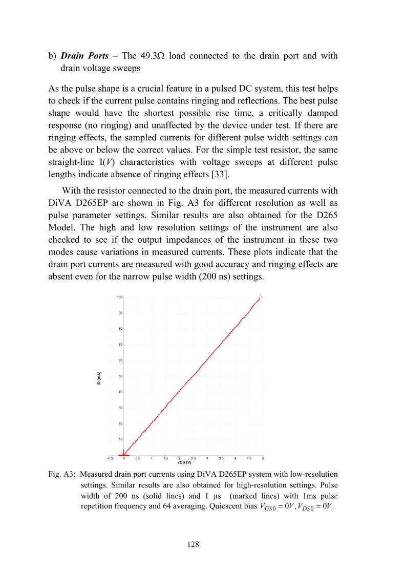
128
b) Drain Ports – The 49.3Ω load connected to the drain port and with drain voltage sweeps
As the pulse shape is a crucial feature in a pulsed DC system, this test helps to check if the current pulse contains ringing and reflections. The best pulse shape would have the shortest possible rise time, a critically damped response (no ringing) and unaffected by the device under test. If there are ringing effects, the sampled currents for different pulse width settings can be above or below the correct values. For the simple test resistor, the same straight-line I(V) characteristics with voltage sweeps at different pulse lengths indicate absence of ringing effects [33].
With the resistor connected to the drain port, the measured currents with DiVA D265EP are shown in Fig. A3 for different resolution as well as pulse parameter settings. Similar results are also obtained for the D265 Model. The high and low resolution settings of the instrument are also checked to see if the output impedances of the instrument in these two modes cause variations in measured currents. These plots indicate that the drain port currents are measured with good accuracy and ringing effects are absent even for the narrow pulse width (200 ns) settings.
Fig. A3: Measured drain port currents using DiVA D265EP system with low-resolution settings. Similar results are also obtained for high-resolution settings. Pulse width of 200 ns (solid lines) and 1 µs (marked lines) with 1ms pulse repetition frequency and 64 averaging. Quiescent bias .VV,VV DSGS 00 00 ==
0 0.5 1 1.5 2 2.5 3 3.5 4 4.5 50-0.5vDS (V)
0
10
20
30
40
50
60
70
80
90
100
iD (m
A)

129
Appendix B
Device Stability in Pulsed I(V) Measurements
The pulsed I(V) characterization of AlGaN/GaN HEMTs for dispersive drain current model derivation described in Chapter 4 requires biasing the device at selected quiescent bias points. These include bias points below pinchoff and in the active region. However, pulsed I(V) measurements from some active quiescent bias points, where gain is high, may lead to device instability.
Stability problems in power FETs are common phenomenon due to the multi-finger layout to attain large gate-periphery. These parallel-connected active devices form many closed loops and cause odd mode oscillations [116]. The symmetry in the device layout makes the possibility of such oscillations suitable.
Due to the high power density of AlGaN/GaN HEMTs, there is also thermal unbalance between inner and outer gate fingers within a large chip. Therefore, this thermally induced electrical unbalance can cause unbalanced-mode loop oscillations [117].
(a)
0 2 4 6 8 10 12 14 16 18 20 22 24 26 28 300-2
vDS (V)
0
50
100
150
200
250
300
350
400
450
500
550
600
650
700
0
-50
iD (m
A)
LimitsvGS=-3(V)vGS=-2.9(V)vGS=-2.8(V)vGS=-2.7(V)vGS=-2.6(V)vGS=-2.5(V)vGS=-1.5(V)vGS=-1.4(V)
vGS=-1.3(V)
vGS=-1.2(V)
vGS=-1.1(V)
vGS=-1(V)
vGS=-0.9(V)
vGS=-0.8(V)
vGS=-0.7(V)
vGS=-0.6(V)
vGS=-0.5(V)
vGS=-0.4(V)
vGS=-0.3(V)
vGS=-0.2(V)
vGS=-0.1(V)
vGS=0(V)

130
(b)
Fig. B1: Stability problems in pulsed I(V) characteristics of a 2 mm AlGaN/GaN on Si HEMT: without (a) and with stabilizing gate resistance (b). The quiescent bias points in the active region are marked with ‘+’.
The techniques used to suppress device oscillations during pulsed I(V) measurements include using series gate resistance and/or shunt resistance across drain-source. But using gate resistance is a better choice, as the gate current is much smaller. Similarly, at the device processing level, partitioning of the gate-feed structure and insertion of isolation resistors [117] (or branched gate feeds [116]) have been devised.
The pulsed I(V) characteristics, from quiescent bias point marked with ‘+’ in Fig. B1(a), for a 2 mm GaN HEMT shows device instability. Improved pulsed I(V) characteristic is shown in Fig. B1(b) for the same device when series gate resistance of 10Ω was used.
0 5 10 15 20 25 30 35 40vDS (V)
0
100
200
300
400
500
600
700
800
iD (m
A)
LimitsvGS=-3(V)vGS=-2.9(V)vGS=-2.8(V)vGS=-2.7(V)vGS=-2.6(V)vGS=-2.5(V)vGS=-2.4(V)
vGS=-1.2(V)vGS=-1.1(V)
vGS=-1(V)
vGS=-0.9(V)
vGS=-0.8(V)
vGS=-0.7(V)
vGS=-0.6(V)
vGS=-0.5(V)
vGS=-0.4(V)
vGS=-0.3(V)
vGS=-0.2(V)
vGS=-0.1(V)
vGS=0(V)
vGS=0.1(V)
vGS=0.2(V)
vGS=0.3(V)
vGS=0.4(V)
vGS=0.5(V)
vGS=0.6(V)
vGS=0.7(V)
vGS=0.8(V)
vGS=0.9(V)
vGS=1(V)

131
References
[1] E. T. Heyen, “Secure Mobile Solutions – Poised for Profitable Growth,” 3GSM Presentation, Infineon, pp. 11, Feb. 2004.
[2] W. Nagy, “Linearity Characteristics of Microwave-Power GaN HEMTs,” IEEE Trans. Microwave Theory Tech., vol. 51, pp. 660-664, Feb. 2003.
[3] Y.-F. Wu et al., “30-W/mm GaN HEMTs by Field Plate Optimization,” IEEE Electron Device Letters, vol. 25, pp. 117-119, March 2004.
[4] K. K. Chu et al., “9.4-W/mm Power Density AlGaN-GaN HEMTs on Free-Standing GaN Substrates,” IEEE Electron Device Letters, vol. 25, pp. 596-598, Sept. 2004.
[5] J. W. Johnson et al., “12 W/mm AlGaN-GaN HFETs on Silicon Substrates,” IEEE Electron Device Letters, vol. 25, pp. 459-461, July 2004.
[6] A. Chini et al., “12 W/mm Power Density AlGaN-GaN HEMTs on Sapphire Substrates,” Electronics Letters, vol. 40, pp. 73-74, Jan. 2004.
[7] A. Wakejima et al., “370 W Output Power GaN-FET Amplifier for W-CDMA Cellular Base Stations,” Electronics Letters, vol. 41, pp. 1371-1373, Dec. 2005.
[8] M. Kanamura et al., “An Over 100W n-GaN/n-AlGaN/GaN MIS-HEMT Power Amplifier for Wireless Base Station Applications,” IEEE Electron Devices Meeting, IEDM Tech. Dig., pp. 572-575, 2005.
[9] R. Therrien et al., “A 36 mm GaN-on-Si HFET Producing 368W at 60V with 70% Drain Efficiency” IEEE Electron Devices Meeting, IEDM Tech. Dig., pp. 568-571, 2005.
[10] K. Joshin, T. Kikkawa, H. Hayashi, T. Maniwa, S. Yokokawa, M. Yokayama, N. Adachi, and M. Takikawa, “A 174W High-Efficiency GaN HEMT Power Amplifier for W-CDMA Base Station Applications,” IEEE Electron Devices Meeting, IEDM Tech. Dig., pp. 983-985, Dec. 2003.
[11] Ph. Bouysse et al., “New Trends in Characterization and Modeling of High Power Devices,” Gallium Arsenide Applications Symposium, GaAs 2001, pp. 24-28, Sept. 2001, London, UK.
[12] J. Vuolevi, Analysis, Measurement and Cancellation of the Bandwidth and Amplitude Dependence of Intermodulation Distortion in RF Power Amplifiers, Doctoral Thesis, Department of Electrical Engineering, University of Oulu, Finland, Nov. 2001.
[13] R. Borges, J. Brown, A. Hanson, S. Singhal, A. Vescan, and P. Williams, “GaN HFETs on Silicon Target Wireless infrastructure Market,” Comput. Semicond., pp. 22–24, Aug. 2003.
[14] C. Weitzel, “Will GaAs Survive for Wireless PA’s??,” in Proceedings of CS-MANTECH, pp. 11-14, 2005.
[15] D. Grinder et al., “Manufacturable GaN HEMT RF Power Technology for Wireless Infrastructure Applications,” in Proceedings of CS-MANTECH, 2004.
[16] P. H. Ladbrooke, MMIC Design: GaAs FETs and HEMTs, Artech House, Inc., Boston, 1989.

132
[17] J. M. Golio, ed., RF and Microwave Semiconductor Device Handbook, CRC press, 2003.
[18] R. J. Trew, “Wide Bandgap Semiconductor Transistors for Microwave Power Amplifiers,” IEEE Microwave Magazine, vol. 1, pp. 46–54, March 2000.
[19] L. F. Eastman and U. K. Mishra, “The Toughest,” IEEE Spectrum, pp. 28-33, May 2002.
[20] R. Steins, New Process Approaches to Metalorganic Vapor Phase Epitaxy of III-nitrides for High Power HEMTs, Doctoral Thesis, Rheinisch-Westfälische Technische Hochschule Aachen, Fakultät für Elektrotechnik und Informationstechnik, Aachen, 2006.
[21] P. Javorka, Fabrication and Characterization of AlGaN/GaN High Electron Mobility Transistors, Doctoral Thesis, Rheinisch-Westfälische Technische Hochschule Aachen, Fakultät für Elektrotechnik und Informationstechnik, Aachen, 2004.
[22] O. Ambacher et al., “Two-dimensional Electron Gases Induced by Spontaneous and Piezoelectric Polarization Charges in N- and Ga-face AlGaN/GaN Heterostructures,” J. Appl. Phy., vol. 48, no. 6, pp. 3222-3233, March 1999.
[23] E. Sarigiannidou et al., “Comparison of Structural Quality in Ga-face and N-face polarity GaN/AlN Multiple-Quantum-Well Structures,” Semicond. Sci. Technol., vol. 21, pp. 612-618, 2006.
[24] Z. Y. Fan et al., “Delta-doped AlGaN/GaN Heterostructure Field-Effect Transistors with Incorporation of AlN Epilayers,” Mat. Res. Soc. Symp. Proc., Materials Research Society, vol. 798, Y10.23.1-Y10.23.5, 2004.
[25] P. M. Asbeck et al., “Piezoelectric Charge Densities in AlGaN/GaN HFETs,” Electronics Letters, vol. 33, pp. 1230–1231, 1997.
[26] S. C. Binari et al., ”Trapping Effects and Microwave Power Performance in AlGaN/GaN HEMTs,” IEEE Trans. Electron Devices, vol. 48, no. 3, pp. 465-470, March 2001.
[27] M. Marso et al., “Influence of carrier supply doping on the RF properties of AlGaN/GaN/SiC high-electron-mobility transistors,” Phys. stat. sol. (c), vol. 2, No. 7, pp. 2611-2614, 2005.
[28] V. Tilak et al., “Influence of Barrier Thickness on the High-Power Performance of AlGaN/GaN HEMTs,” IEEE Trans. Electron devices, vol. 48, no. 3, pp. 504-506, Nov. 2001.
[29] T. Kikkawa el al., “Recent Progress of Highly Reliable GaN-HEMT for Mass Production,” in Proceedings of CS-MANTECH, pp. 171-174, April 2006.
[30] J. Würfl, “GaN - Hochfrequenzelektronik,” Workshop GaN-Elektronik, Bonn, April 2002.
[31] R. Lossy et al., “Large Area AlGaN/GaN HEMTS Grown on Insulating Silicon Carbide Substrates,” Phys. stat. sol. (a) 194, No. 2, pp. 460-463, 2002.
[32] G. Menghesso et al., “Surface-Related Drain Current Dispersion effects in AlGaN/GaN HEMTs,” IEEE Trans. Electron Devices, vol. 51, no. 10, pp. 1554-1561, Oct. 2004.

133
[33] P. H. Ladbrooke, Pulsed I(V) Measurement of Semiconductor Devices with Applications, Accent Optical Technologies, Inc., 2004.
[34] Y.-F. Wu et al., “High-Gain Microwave GaN HEMTs with Source-Terminated Field-Plates,” IEEE Int. Electron Devices Meeting (IEDM) Tech. Dig., pp. 1078-1079, 2004.
[35] Y. Ando et al., “12W/mm Recessed Gate AlGaN/GaN Heterojunction Field-Plate FET,” IEEE Int. Electron Devices Meeting (IEDM) Tech. Dig., pp. 565-566, 2003.
[36] L. Shen et al., “High-Power Polarization-Engineered GaN/AlGaN/GaN HEMTs Without Surface Passivation,” IEEE Electron Device Letters, vol. 25, no. 1, pp. 7-9, Jan. 2004.
[37] A. Koudymov et al., “Mechanism of Current Collapse Removal in Field-Plated Nitride HFETs,” IEEE Electron Device Letters, vol. 26, no. 10, pp. 704-706, Oct. 2005.
[38] F. Yamaki et al., “Leakage Current Screening for AlGaN/GaN HEMT Mass-Production,” in Proceedings of CS-MANTECH, pp. 95-98, May 2007.
[39] J. Lee et al., “Post-Annealing Effects on Device Performance of AlGaN/GaN HFETs,” Solid-State Electronics, vol. 48, pp. 1855-1859, 2004.
[40] R. Frensley, “Power Limiting Breakdown Effects in GaAs MESFETs,” IEEE Trans. Electron Devices, vol. ED-28, pp. 962-970, August 1981.
[41] R. Williams, Modern GaAs Processing Methods, © 1990 Artech House Inc. Norwood.
[42] J. M. Golio, Microwave MESFETs and HEMTs, © 1991 Artech House Inc. Norwood, 1991.
[43] E. M. Chumbes et al., “AlGaN/GaN high Electron Mobility Transistors on Si(111) Substrates,” IEEE Trans. Electron Devices, vol. 48, no. 3, pp. 420-425, March 2001.
[44] J. P. Teyssier et al., “A Pulsed S-parameters Measurement Setup for the Non-linear Characterization of FETs and Bipolar Power Transistors,” 23th European Microwave Conf., pp. 489-493, Sept. 1993.
[45] A. Parker et al., “Determining Timing for Isothermal Pulsed-Bias S-Parameter Measurements,” IEEE MTT-S Int. Microwave Symp. Dig., pp. 1707-1710, 1996.
[46] M. Berroth and R. Bosch, “High-Frequency Equivalent Circuit of GaAs FETs for Large-Signal Applications,” IEEE Trans. Microwave Theory Tech., vol. 39, pp. 224-229, Feb. 1991.
[47] H. Kondoh, “An Accurate FET Modeling from Measured S-parameters,” IEEE MTT-S Int. Microwave Symp. Dig., pp. 377-380, 1986.
[48] J. W. Bandler and Q. J. Zhang, “An Automatic Decomposition Technique for Device Modeling and Large Circuit Design,” IEEE MTT-S Int. Microwave Symp. Dig., pp. 709-712, 1987.
[49] F. Lin and G. Kompa, “FET Model Parameter Extraction Based on Optimization with Multiplane Data-Fitting and Bidirectional Search - A New Concept,” IEEE Trans. Microwave Theory Tech., vol. 42, pp. 1114-1120, July 1994.

134
[50] W. N. Mwema, A Reliable Optimization-based Model Parameter Extraction Approach for GaAs-based Field-Effect Transistors using Measurement-correlated Parameter Starting Values, Doctoral Thesis, Department of High Frequency Engineering, University of Kassel, Germany, 2002.
[51] G. Dambrine et al., “A New Method for Determining the FET Small-Signal Equivalent Circuit,” IEEE Trans. Microwave Theory Tech., vol. 36, pp. 1151-1159, July 1988.
[52] P. M. White et al., “Improved Equivalent Circuit for Determination of MESFET and HEMT Parasitic Capacitances from “Cold-FET” Measurements,” IEEE Microwave and Guided Wave Letters, vol. 3, pp. 453-454, Dec. 1993.
[53] J. Wood and D. Root, “Bias-Dependent Linear Scalable Millimeter-Wave FET Model,” IEEE Trans. Microwave Theory Tech., vol. 48, pp. 2352-2360, Dec. 2000.
[54] R. Tayrani et al., “A New and Reliable Direct Parasitic Extraction Method for MESFETs and HEMTs,” 23th European Microwave Conf., pp. 451–453, Sept. 1993.
[55] C. Camacho-Peñalosa et al., “On Negative Drain-to-source Capacitances in Microwave FET-type Devices,” Proc. 8th Int. Symp. Microwave and Optical Technologies (ISMOT’01), pp. 115-118, June 2001.
[56] G. Kompa and M. Novotny, “Frequency-dependent Measurement Error Analysis and Refined FET Model Parameter Extraction Including Bias-dependent Series Resistors,” Int. IEEE Workshop on Experimentally Based FET Device Modeling & Related Nonlinear Circuit Design, Kassel University, Department of High Frequency Engineering, pp. 6.1-6.16, July 1997.
[57] N. Rorsman et al., “Accurate Small-Signal Modeling of HFETs for Millimeter-Wave Applications,” IEEE Trans. Microwave Theory Tech., vol. 44, pp. 432-437, March 1996.
[58] R. Quay et al., “Nonlinear Electronic Transport and Device Performance of HEMTs,” IEEE Trans. Electron Devices, vol. 48, no. 2, pp. 210-217, Feb. 2001.
[59] J. Wood and D. Root, “A Symmetric and Thermally De-embedded Nonlinear FET Model for Wireless and Microwave Applications,” IEEE MTT-S Int. Microwave Symp. Dig., pp. 35-38, 2004.
[60] R. Anholt, Electrical and Thermal Characterization of MESFETs, HEMTs, and HBTs, Artech House, Boston, 1995.
[61] W.R. Curtice, “A MESFET Model for Use in the Design of GaAs Integrated Circuits,” IEEE Trans. Microwave Theory Tech., vol. 28, pp. 448-456, May 1980.
[62] Y. Tajima, B. Wrona, and K. Mishima, “GaAs FET Large-Signal Model and Its Application to Circuit Designs,” IEEE Trans. on Electron Devices, vol. 28, pp. 171-175, February 1981.
[63] A. Materka and T. Kacprzak, “Computer Calculation of Large-Signal GaAs FET Amplifier Characteristics,” IEEE Trans. Microwave Theory Tech., vol. 33, pp. 129-135, February 1985.

135
[64] H. Statz et al., “GaAs FET Device and Circuit Simulation in SPICE,” IEEE Trans. on Electron Devices, vol. 34, pp. 160-169, February 1987.
[65] I. Angelov et al., “A New Empirical Nonlinear Model for HEMT and MESFET Devices,” IEEE Trans. Microwave Theory Tech., vol. 40, pp. 2258-2266, Dec. 1992.
[66] Y. Tajima, ”Progress in RF Device Modeling: From MESFETs to GaN pHEMTS,” The Annual RF & Microwave Solutions Update, pp. 40-44, July 2006.
[67] D. E. Root, S. Fan, and J. Meyer, "Technology-Independent Large-Signal FET Models: A Measurement-Based Approach to Active Device Modeling," Proceedings of 15th ARMMS Conf., Sept. 1991.
[68] J. Wood and D. Root, “‘Agilent-Angelov’ III-V FET Model,” Technical Presentation in Device Modeling Seminar, Japan, Oct. 2005.
[69] V. Cuoco et al., “The ‘Smoothie’ Data Base Model for Correct Modeling of Non-linear Distortion in FET Devices,” IEEE MTT-S Int. Microwave Symp. Dig., pp. 2149-2152, 2002.
[70] J. Xu et al., “Neural-Based Dynamic Modeling of Nonlinear Microwave Circuits,” IEEE Trans. Microwave Theory Tech., vol. 50, pp. 2769-2780, Dec. 2002.
[71] S. A. Maas, “How to Model Intermodulation Distortion,” IEEE MTT-S Int. Microwave Symp. Dig., pp. 149-151, 1991.
[72] J. C. Pedro and J. Perez, “Accurate Simulation of GaAs MESFET’s Intermodulation Distortion Using a New Drain-Source Current Model,” IEEE Trans. Microwave Theory Tech., vol. 42, pp. 25-33, Jan. 1994.
[73] S. A. Maas, “Amplifiers and Oscillators: The Landscape in 2007,” Microwave Journal, pp. 24-44, April 2007.
[74] J. Brinkhoff and A. Parker, “Effect of Baseband Impedance on FET Intermodulation,“ IEEE Trans. Microwave Theory Tech., vol. 51, pp. 1045-1051, March 2003.
[75] J. F. Sevic et al., “A Novel Envelope Termination Load-Pull Method for ACPR Optimization of RF/Microwave Power Amplifier,“ IEEE MTT-S Int. Microwave Symp. Dig., pp. 723-726, 1998.
[76] J. Cha et al., “Optimum Design of Predistortion RF Power Amplifier for Multicarrier WCDMA Applications,” IEEE Trans. Microwave Theory Tech., vol. 52, pp. 655-663, Feb. 2004.
[77] I. Schmale, Entwicklung eines konsistenten elektrothermischen Großsignalmodells für Feldeffekttransistoren als Grundlage für den zuverlässigen Entwurf monolithischer Frequenzverdoppler, Doctoral Thesis, Department of High Frequency Engineering, University of Kassel, Kassel, Germany, Sept. 1999.

136
[78] D. E. Root and B. Hughes, “Principles of Nonlinear Active Device Modeling for Circuit Simulation,” Proc. 32nd ARFTG Conf., Tempe, AZ, pp. 3-26, Dec. 1988.
[79] S. Piotrowicz et al., “A Simplified Approach to Determine a Small Signal Equivalent Circuit up to 60 GHz,” Int. IEEE Workshop on Experimentally Based FET Device Modeling and Related Nonlinear Circuit Design, University of Kassel, Germany, pp. 3.1-3.8, July 1997.
[80] F. Filicori et al., “A 'Backgating' Model Including Self-Heating for III-V FETs," IEEE Gallium Arsenide and Related III/V Compounds Application Symp., pp. 462-467, Amsterdam 1998.
[81] K. Jeon, Y. Kwon, and S. Hong, “A Frequency Dispersion Model of GaAs MESFET for Large-signal Applications,” IEEE Microwave and Guided Wave Letters, vol. 7, no. 3, pp. 78-80, March 1997.
[82] X. Hu et al., “Si3N4/AlGaN/GaN-Metal-Insulator-Semiconductor Heterostructure Field-Effect Transistors,” Appl. Phy. Lett., vol. 79, pp. 2832- 2834, Oct. 2001.
[83] P. McGovern et al., “Experimental Investigation of DC-RF Dispersion in AlGaN/GaN HFET’s Using Pulsed I-V and Time-Domain Waveform Measurements,” in Proceedings of CS-MANTECH, April 2005.
[84] J. Park et al., “Thermal Modeling and Measurement of AlGaN-GaN HFETs Built on Sapphire and SiC Substrates,” IEEE Trans. Electron Devices, vol. 51, no. 11, pp. 1753-1759, Nov. 2004.
[85] A. Santarelli et al., “Equivalent-Voltage Description of Low-Frequency Dispersive Effects in Large-Signal FET Models,” Proc. of GaAs 2001, Sept. 2001, London, UK.
[86] K. Koh et al., “A Large-Signal FET Model Including Thermal and Trap Effects with Pulsed I-V Measurements,” IEEE MTT-S Int. Microwave Symp. Dig., pp. 467-470, 2003.
[87] D. Siriex et al., “Characterization and Modeling of Nonlinear Trapping Effects in Power SiC MESFETs,” IEEE MTT-S Int. Microwave Symp. Dig., vol. 2, pp. 765-768, 2000.
[88] F. Filicori et al., “Empirical Modeling of Low-Frequency Dispersive Effects due to Traps and Thermal Phenomena in III-V FETs,” IEEE Trans. Microwave Theory Tech., vol. 43, pp. 2972-2981, Dec. 1995.
[89] A. F. M. Anwar et al., “Temperature Dependent Transport Properties in GaN, AlxGa1-xN, and InxGa1-xN Semiconductors,” IEEE Trans. Electron Devices, vol. 48, no. 3, pp. 567-572, March 2001.
[90] G. Kompa, “Modeling of Dispersive Microwave FET Devices Using a Quasi-Static Approach,” Int. Journal of Microwave and Millimeter Wave CAE, vol. 5, no. 3, pp. 173-194, 1995.
[91] C. Camacho-Penalosa and C. S. Aitchison, “Modeling Frequency Dependence of Output Impedance of a Microwave MESFET at Low Frequencies,” Electronic Letters, vol. 21, pp. 528-529, 1985.

137
[92] J. M. Golio et al., “Frequency-Dependent Electrical Characteristics of GaAs MESFETs,” IEEE Trans. Electron Devices, vol. 37, no. 5, pp. 1217-1227, May 1990.
[93] J. Staudinger, M. C. de Baca and R. Vaitkus, “An Examination of Several Large Signal Capacitance Models to Predict GaAs HEMT Linear Power Amplifier Performance,” IEEE Radio and Wireless Conference Proceedings, pp. 343-346, Aug. 1998.
[94] D. E. Root, “Nonlinear Charge Modeling for FET Large-Signal Simulation and Its Importance for IP3 and ACPR in Communication Circuits,” Proc. IEEE Midwest Symposium on Circuit and Systems, vol. 2, pp. 768–772, 2001.
[95] W. Struble et al., “A New Small Signal MESFET and HEMT Model Compatible With Large Signal Modeling,” IEEE MTT-S Int. Microwave Symp. Dig., pp. 1567-1570, 1994.
[96] J.-W. Lee and K. J. Webb, “A Temperature-Dependent Nonlinear Analytic Model for AlGaN-GaN HEMTs on SiC,” IEEE Trans. Microwave Theory Tech., vol. 52, pp. 2-9, Jan. 2004.
[97] C. J. Wei et al., “Completely Consistent ‘No-Charge’ pHEMT Model Including DC/RF Dispersion,” IEEE MTT-S Int. Microwave Symp. Dig., pp. 2133-2136, 2002.
[98] F. Follmann et al., “Consistent Large Signal Implementation of Capacitances Driven by Two Steering Voltages for FET Modeling,” 35th European Microwave Conf., pp. 1149–1151, Oct. 2005.
[99] I. Schmale and G. Kompa, “A Physics-based Non-linear FET Modeling Including Dispersion and High Gate-forward Currents,” Int. IEEE Workshop on Experimentally Based FET Device Modeling & Related Nonlinear Circuit Design, pp. 27.1-27.7, University of Kassel, 1997.
[100] D. E. Root, “A Measurement-Based FET Model Improves CAE Accuracy,” Microwave Journal, pp. 126-139, Sept. 1991.
[101] J. M. Collantes et al., “A New Large-Signal Model Based on Pulse Measurement Techniques for RF Power MOSFET,” IEEE MTT-S Int. Microwave Symp. Dig., pp. 1553-1556, 1995.
[102] K. Fujii, “An Improved GaAs MESFET Model for the Pulsed I-V Measurement,” IEEE MTT-S Int. Microwave Symp. Dig., pp. 615-618, 1995.
[103] A. K. Jastrzebski, “Characterization and Modeling of Temperature and Dispersion Effects in Power MESFETs,” 24th European Microwave Conference, pp. 1319-1324, 1994.
[104] K. Fujii et al., “Accurate Modeling for Drain Breakdown Current of GaAs MESFETs,” IEEE Trans. Microwave Theory Tech., vol. 47, pp. 516-518, April 1999.
[105] D. Denis, C. M. Snowden and I. C. Hunter, “Design of Power FETs Based on Coupled Electro-Thermal-Electromagnetic Modeling,” IEEE MTT-S Int. Microwave Symp. Dig., pp. 461-464, 2005.
[106] F. Bonani and G. Ghione, “On the Application of the Kirchhoff Transformation to the Steady-State Thermal Analysis of Semiconductor Devices with

138
Temperature-Dependent and Piecewise Inhomogeneous Thermal Conductivity,” Solid-State Electronics, vol. 38, no. 7, pp. 1409-1412, 1995.
[107] D. Morelli et al., “Carrier Concentration Dependence of the Thermal Conductivity of Silicon Carbides,” Inst. Phys. Conf. Ser., vol. 137, pp. 313-315, 1993.
[108] W. B. Joyce, “Thermal Resistance of Heat Sinks with Temperature-Dependent Conductivity,” Solid-State Electronics, vol. 18, no. 3, pp. 321-322, 1975.
[109] R. Gaska et al., “Self-Heating in High-Power AlGaN-GaN HFETs,” IEEE Electron Device Letters, vol. 19, pp. 89-91, March 1998.
[110] I. Schmale and G. Kompa, “Integration of Thermal Effects into Table-Based Large-Signal FET Model,” 28th European Microwave Conference, pp. 102-107, Oct. 1998.
[111] A. M. Darwish et al., “Thermal Resistance Calculation of AlGaN-GaN Devices,” IEEE Trans. Microwave Theory Tech., vol. 52, pp. 2611-2619, Nov. 2004.
[112] H. F. Cooke, “Precise Technique Finds FET Thermal Resistance,” Microwave & RF, pp. 85-87, August 1986.
[113] S. –S. Lu et al., “The Origin of the Kink Phenomenon of Transistor scattering parameter S22,” IEEE Trans. Microwave Theory Tech., vol. 49, pp. 333-340, Feb. 2001.
[114] F. van Raay and G. Kompa, “A 40 GHz Large-Signal Double-Reflectometer Waveform Measurement System Designed for Load-Pull Applications,” 26th European Microwave Conference, pp. 657-661, 1996.
[115] E. S. Mengistu and G. Kompa, “A Large-Signal Model of GaN HEMTs for Linear High Power Amplifier Design,” 36th European Microwave Conference, pp. 292-295, 2006.
[116] S. Goto et al, “Stability Analysis and Layout Design of an Internally Stabilized Multi-Finger FET for High-Power Base Station Amplifiers, ” IEEE MTT-S Int. Microwave Symp. Dig., pp. 229-232, 2003.
[117] K. Yamanaka et al, “S and C band Over 100W GaN HEMT 1-chip High Power Amplifiers with Cell Division Configuration,” 13th GAAS® Symp., pp. 241-244, 2005.
[118] A. Kricke, private communication, Fachgebiet Technische Elektronik, Universität Kassel, Sep. 2007.


