Page 1
APPROVED:
Hyoung Soo Kim, Major Professor Hualiang Zhang, Committee Member Gayatri Mehta, Committee Member Shengli Fu, Committee Member and
Chair of the Department of Electrical Engineering
Kuruvilla John, Associate Dean of the College of Engineering
Costas Tsatsoulis, Dean of the College of Engineering
Mark Wardell, Dean of the Toulouse Graduate School
RELIABILITY OF ELECTRONICS
Larry E. Wickstrom
Thesis Prepared for the Degree of
MASTER OF SCIENCE
UNIVERSITY OF NORTH TEXAS
December 2014
Page 2
Wickstrom, Larry E. Reliability of Electronics. Master of Science (Electrical
Engineering), December 2014, 51 pp., 16 figures, bibliography, 10 titles.
The purpose of this research is not to research new technology but how to
improve existing technology and understand how the manufacturing process works.
Reliability engineering falls under the category of quality control and uses predictions
through statistical measurements and life testing to figure out if a specific manufacturing
technique will meet customer satisfaction. The research also answers choice of
materials and choice of manufacturing process to provide a device that will not only
meet but exceed customer demand. Reliability engineering is one of the final testing
phases of any new product development or redesign.
Page 3
ii
Copyright 2014
by
Larry E. Wickstrom
Page 4
ACKNOWLEDGEMENTS
Over the past three years I have enjoyed working with Prof. Hyoung Soo Kim as
my advisor and I would like to thank him for all his guidance and support over the
course of my Graduate Studies at the University of North Texas. I would also like to
thank Prof’s Shengli Fu, Hualiang Zhang, and Gayatri Mehta for taking part as members
of my thesis committee and for having me in their classes.
iii
Page 5
TABLE OF CONTENTS
ACKNOWLEDGEMENTS ............................................................................................... iii
LIST OF FIGURES .......................................................................................................... v
CHAPTER 1 INTRODUCTION ........................................................................................ 1
CHAPTER 2 DISCRETE COMPONENTS ...................................................................... 7
CHAPTER 3 PARASITIC EFFECTS ON ELECTRONICS ............................................ 12
CHAPTER 4 COMPONENT RELIABILITY .................................................................... 22
CHAPTER 5 MATERIALS USED IN SEMICONDUCTORS .......................................... 38
CHAPTER 6 DIGITAL TECHNOLOGY ........................................................................ 45
BIBLIOGRAPHY ........................................................................................................... 51
iv
Page 6
LIST OF FIGURES
Figure 3.1 Leakage over time .................................................................................... 15
Figure 3.2 Leakage current over extended periods ................................................... 15
Figure 3.3 Leakage current over time and temperature ............................................ 16
Figure 3.4 Plexiglas after breakdown voltage limit was applied and reached ............ 17
Figure 3.5 Illustration of the hydraulic analogy .......................................................... 18
Figure 3.6 Ideal vs. noisy waveforms ........................................................................ 20
Figure 3.7 High pass and low pass circuit examples ................................................. 21
Figure 3.8 Rectified AC waveform ............................................................................. 22
Figure 4.1 Capacitor types and typical values ........................................................... 28
Figure 4.2 Simple parallel plate capacitor design ...................................................... 29
Figure 4.3 Multi-layer ceramic chip capacitor cross section ...................................... 30
Figure 4.4 Defects of chip capacitors due to high temp or high wattage ................... 30
Figure 4.5 Internal components of an electrolytic capacitor ...................................... 34
Figure 4.6 Capacitance over temperature ................................................................. 36
Figure 4.7 Examples of failed electrolytic capacitors ................................................. 37
Figure 4.8 Electrolytic capacitor lifespan over temperature ....................................... 38
v
Page 7
CHAPTER 1
INTRODUCTION
Why do electronic devices behave differently when running at full capacity or in
abnormal environmental conditions?
The purpose of this study is to look at common knowledge about electronics and
quantify it with data and in detailed explanations. This area of research mostly covers
reliability or quality assurance (QA) engineering topics. I chose these topics because
this has been an important part of my jobs in industry over the past decade. Another
very important topic covered is the parts designed for specific applications that require
heavy stress, load, or extreme environmental conditions.
So far, silicon has been the main base material for semiconductor devices and
has been an industry standard since the invention of the transistor as well as other solid
state electronics. This is because silicon is a pure element and does not present the
flaws and issues that compound base materials like gallium arsenide (GaAs) do. Other
materials and elements can be introduced, or doped, into silicon without affecting its
material or crystal lattice structure. Silicon with these added materials presents many
problems that need to be addressed in order to prevent usage failures.
The upcoming issue with silicon is that its theoretical switching distance limit is
about to be reached. Physicists have claimed that 10nm is the theoretical limit that a
charge can be transferred from point to point, making 5nm lithography on silicon the
lowest known possible transistor line size. At this point, 22nm technology, and soon
14nm, will be readily available to the public. This is why other materials, like GaAs, are
being researched with faster switching potential and smaller transistor sizes. Not only
1
Page 8
are different materials being looked into but also new switching methods and transistor
shapes on new materials and existing silicon are also being researched because the
5nm limit is well known and new solutions are always being found.
Another piece of common knowledge is Ohm’s Law: I = V/R, everyone in the
engineering field knows of this and its mathematical properties. However there is a
major difference between an ideal mathematical situation and a real world situation.
Some devices focus on current values and some on voltage values but the resistance is
the constant that is dialed in to affect one or the other (Power (W) is an effect of I*V and
is included in this) in its operation. However resistance will change under different
conditions affecting the other components of the desired result.
A semiconductor is what the name says, it is neither a full conductor or insulator.
It performs according to the materials introduced and the charges applied. Every
material, even full metal conductors like copper, have resistance. These materials are
affected by heat, stress, and wear. As it is well known when materials heat up they
expand and the reverse for cooling and when materials expand the resistance also goes
up. Now when you look at a semiconductor feature say from 25C to 85C in temp it does
not expand that much maybe a few nanometers or microns depending on the feature
size, right? Now when you have a chip that has millions or billions or transistors all
expanding and contracting based on current flow or environment then it becomes a big
deal.
Switching speeds and amount of current are one of the major sources for heat in
chips. This added with heat buildup from processing and outside environmental heat or
cold can add to complications in design. This is where a specific design or
2
Page 9
recommended usage rating comes from. Most consumer grade products are rated for
0C to 85C in that range but other uses will require either a different or wider range. This
is where the choice of materials, design structure, and design parameters play a large
role.
The purpose of this research is to quantify common knowledge. As stated before
most consumer grade products have a specific operating temperature and humidity
rating. The reason the range is limited, compared to others, for consumer use is for
reasons of cost and device yield in fabrication. Commercial, industrial, or automotive
requirements are much stricter. In this the cost per device goes up. The same chip rated
for consumer grade can cost much more per chip with wider requirement needs. In the
case for automotive, safety and reliability is the largest concern and special precautions
must be taken to insure higher quality and operating range.
As for cost, I am sure the readers have heard about microchips ranging in the
five to seven figure cost range and think to themselves: “How is this possible when I can
pick up an Intel CPU for $100 at Fry’s electronics?” The reason is that the same chip is
required to have either: a much lower margin of error during test, a customer specific
addition or application, or require an operating range so extreme that the average
consumer cannot comprehend it. Let’s take a chip that is needed for satellite, in outer
space the temperature can range from absolute zero (-273C) to much higher temps
along with unblocked radiation. It is very difficult to test these conditions and when
tested, only a small percentage of chips will survive probe, final, or field testing.
All the added outside effects can alter the operation of any chip more so in
analog devices than others. Analog technology requires precision for precision values is
3
Page 10
how analog processing works. Analog is a continuous signal sent through any medium
most by wire or by air. The signal needs to be read properly which is where the noise
and interference factors come in. Before digital technology came along analog
processing required a lot of filtering for error correction without the aid of digital
processing. This was usually in the form of a lot of resistors, capacitors, inductors, and
other discrete devices. Hence the reason why high tech was so expensive pre-dating
digital (take inflation into consideration).
To obtain perfect point to point analog transmission with no errors became more
expensive the further the distance was. This is why most consumer products (I’m
thinking 1980s and before here) allowed a certain amount of error to occur to keep
costs down. For those who remember how important TV signal reception was before
cable TV came in will know how imperfect an over the air transmission was, especially
for those who lived far enough away from the station antenna. The static showed the
error I am speaking of, anything from bad weather to white noise could interfere with the
point to point transmission over distance. This on top of the fact that most consumer
grade parts did not last nearly as long as they did now due to heat, usage, and high
energy requirements lead to the desire for digital technology.
Digital technology became main stream in the consumer market in the 1990s.
Even though digital technology was around much longer and beginning to creep into the
market earlier, the mid1990s is when digital technology really took off. Digital is what the
word represents: the use of digits for calculations. Digital technology makes use of
discrete values, mostly in the form of binary numbers representing a 1 or 0. In
semiconductors the 1 and 0 values are represented by a set voltage, usually ground is
4
Page 11
the 0 and the supply voltage is the 1. Digital offers a solution compared to analog in
terms of margin of error and error correcting. A voltage range can be set to represent a
high or low value eliminating the need for a precision value. Calculating binary values
helps make error correcting much easier and cheaper since the need for discrete
components required for analog filtering and processing is greatly reduced.
Digital processing has improved greatly over the last decade. Digital filtering and
processing are two techniques have improved. The improvements come at a cost,
higher clock speeds and constant re-designs are required to meet the demand. TDP or
thermal design power has been an issue in processing for some time. Since lithography
sizes are decreasing more transistors are capable of fitting in modern CPUs this means
more switching operations per second are taking place hence higher power
consumption. One benefit of smaller transistor size is lower power consumption per
transistor but with the multiplied count of transistors the natural lower power
consumption is not enough. Voltage settings have also decreased to compensate for
the overall wattage within but this required major changes in transistor design to be
used at lower levels. At one point in time 5 volts was the standard for digital switching;
now we are as low as 1-1.5V. Smaller transistor sizes and lower power usage also
introduce more design complications but this is discussed later on. To sum up the TDP
issue a CPU that now uses 1-1.5V consumes a total of 70-150 watts on standard
desktop applications to give an idea on how much goes on in modern CPUs.
While digital technology offers a more accurate and cost effective solution in
some cases it is not a replacement for analog technology. With wireless technology
becoming more widespread the demand for analog technology surged back. Digital DC
5
Page 12
voltage levels cannot be transmitted over the air, it requires a discrete or continuous
wave to do it which is why analog is required. However it is possible to send a specific
analog signal with a digital representation over the air. This is one example of why both
technologies are needed and how they are used together. There are also other ways
multiple technologies can help complement one another. There are more examples in
the sections that follow.
6
Page 13
CHAPTER 2
DISCRETE COMPONENTS
A major part of analog and digital technology is the use of discrete components.
In design we often think of the mathematical representation of these components and
the effects that they will produce. In practice other design methods are added to insure
device reliability and component lifespan.
Resistance is always present in any discrete component or material, though the
resistance is dependent on the operation of the component and materials used. The
basic carbon resistor and copper wire are good examples to start out with because they
are used in just about every electronic device and the resistance is relatively simple to
understand and it is not affected by as many factors. Even though the readers are likely
to know this, wires are used to conduct electrical current and resistors are used to
restrict the flow of electrical current.
Temperature dependence is one of the factors that affects the value of resistance
and can affect device performance depending on the accuracy required. In most clean
rooms, server rooms, laboratories, etc the environment is temperature controlled for
this very reason. Room temperature is usually defined as 20 or 25 degrees Celsius
which is 68 to 77 Fahrenheit. Most controlled environments I have been in use 70F or
20C as room temperature since it is a common standard for calculations.
Every material used has a resistance and temperature coefficient, in wire copper
is commonly used and in resistors carbon is used as stated before. Assuming we have
materials with no impurities the electrical resistance of a wire is:
7
Page 14
R = ρL/A
R = Resistance (Ω), ρ = Resistivity Coefficient (Ωm), L = Length of Wire (m), A = Cross
section area of wire (m2)
Take 10 gauge wire which is the largest that will be commonly seen the cross
section of the area is 2.59mm (5.26mm2), 1 meter of wire, and a coefficient for copper is
1.724 * 10-8.
R = (1.724*10-8 * 1m)/(5.26mm2 * 10-6 m2/mm2) = 3.277 * 10-3 Ω over 1m of 10
gauge wire.
For 1m of 20 gauge which is commonly used in electronics (most cases smaller):
R = (1.724*10-8 * 1m)/(0.518mm2 * 10-6 m2/mm2) = 33.281 * 10-3 Ω over 1m of 20
gauge wire.
Even though the resistance is not high over copper wire this shows that 20 gauge
has 10x the resistance of 10 gauge wire over the same distance. This directly affects
the maximum ampere rating for wire for power transmission, 10 gauge has a 15A rating
and 20 gauge has a 1.5A rating. However there is a trade off in the terms of maximum
frequency where 10 gauge can transmit 2600Hz and 20 gauge can transmit 26kHz
which is why smaller gauge wire is desired in electronics but distance must always be
accounted for. (Source: American Wire Gauge Standard.)
Over temperature these ratings change. It is not only important to know for
reasons of environment but also when wattage is transmitted over any discrete
component the temperature of it will go up. Since carbon resistors are set by the
manufacturer I will not go into specifics of the dimensions of the carbon film to set
resistance. Copper wire will also change in resistance over temperature, this is the
8
Page 15
exact reason why max ampere rating for wire is much lower than its full potential, 15
amps going over a 10 gauge wire will make it very hot.
Every material has a temperature coefficient that shows the change in resistance
over temperature. I will use the 1m of 20 gauge of copper wire and a 50 Ω carbon
resistor to show how temperature can affect their mathematical representation.
ΔR = α*ΔT
ΔR is the change in resistance, α is the temperature coefficient, and ΔT is the
change in temperature
1m of 20 gauge wire = 33.281 mΩ: (Copper’s coefficient is 4.29*10-3)
We will assume 20C as our starting point and show the resistance value at 85C.
ΔR = (4.29*10-3)*(85-20) = 0.27885, R = R0*(1+ ΔR), R @ 85C = 42.561mΩ, this
is 25% increase in resistance.
For a 50 Ω Carbon resistor:
ΔR = (-4.8*10-4)*(85-20) = -0.0312, R = R0*(1+ ΔR), R @ 85C = 48.44Ω, this is
3% decrease in resistance.
Some applications require precision values for various reasons and the values
represented demonstrate why application dictates design and materials. Though most
electronics will never see temperatures of 85C it is usually the maximum specified
temperature for a lot of applications. In the case of precision electronics, especially in
analog technology, these deviations in value need to be controlled or have an allowed
tolerance for error. Even though some components can be manufactured to within
0.00001% of the specified value or better, environment and use can alter precision no
matter what, this is very important when it comes to electronic reliability because
9
Page 16
hundreds to millions of components can be used in an electronic system and any one
system can affect the others.
An inductor is another form of a discrete component. The purpose of inductors
range from radio frequency (RF) chokes, power supply rectification, and power
transformers (the process of converting AC to DC electricity). An inductor simply is a
wire wrapped around a magnet combining conduction and magnetic flux. An inductor
does not have a direct current resistance level in ohms but contributes to system
impedance, impedance is a set resistance based on frequency.
Inductors gain in impedance levels when the frequency increases; this is why
they are used as radio frequency (RF) chokes because they can reject certain
frequencies based on design, though inductors are generally used to reject higher
frequencies. Inductors are also used in power supplies to control the flow of electricity
and help prevent any undesired effects such as ripple current. Inductors are generally
used in analog circuits for the purpose of blocking AC or signal energy and allowing DC
to pass. Inductors are a robust component but are not immune to deviations as wires
and resistors are. Environment and current flow affect the values on the device, take the
wire deviation mentioned above along with changes in magnetic flux over temp
humidity, etc. a tolerance needs to be stated for practical design in precision electronics
or power supplies.
When it comes to wires, resistors, and inductors they have a long life span due to
being a solid material and studies in reliability generally focus on handling power and
accuracy and in the case of inductors the life of the magnetic flux. Since all three of
10
Page 17
those components allow DC current to pass controlling and rating power usage is
important as to not destroy them or shorten their lifespan.
Capacitors are another form of discrete component but unlike the previous
components mentioned capacitors are very volatile component and can fail for a wide
variety of reasons. The study of reliability of passive and discrete components has the
most focus on capacitors.
A Capacitor is a component that stores a charge and discharges in set intervals
at specified voltages and in some cases specified frequencies and polarities. The
impedance rating for a capacitor goes down at higher frequencies, the only difference is
that it goes down at a non-linear rate. At 0Hz which is the operating frequency of DC
current its resistance is supposed to be infinite, in other words a DC block. However this
is only an ideal situation, not a real one.
There are many designs of capacitors but the simplest one to explain is the
parallel plate capacitor. It is two conducting plates separated by dielectric material. A
dielectric is an insulator designed for a specific purpose which is usually rated to allow
electrical fields to move in a certain manner. A common example of a dielectric is seen
in coaxial cables, the purpose of that dielectric is to confine the signal energy to the
solid core of the cable to prevent signal loss and to separate the core from the shield
outside of it. As stated dielectrics can be designed to pass a certain charge or reject it,
this is what separates a dielectric from what most people perceive to be a common
insulator.
11
Page 18
CHAPTER 3
PARASITIC EFFECTS ON ELECTRONICS
In design and learning concepts of electronics we learn them by understanding
the ideal situations. In the real world there are many parasitic effects or limitations that
do not allow ideal or designed specifications to work. Additional testing and design is
required to achieved a desired effect.
Some of the issues that surround overall device reliability and accuracy are:
• Leakage current
• Noise
• Ripple Current
• Temperature
• Environmental effects
• Design
Leakage current is one of the most common issues in electronics. It is very
undesirable for many reasons. One reason is that in circuit design there are points in
the circuit where DC current is unwanted, this is one reason why capacitors are used as
DC blocks. Another reason is that in some circuit designs, an op-amp is one example,
no current is to enter or leave it to properly amplify the signal energy introduced.
Leakage current can also shorten battery life, batteries have a set usage rating and will
remain active even when the device is turned off. When current is allowed to leak
through various components the charge in the battery will find a route to ground even
when the device is turned off, hence leakage. Though the effects of leakage current are
minimal in the short run and will not immediately cause failure, in the long run and in the
12
Page 19
terms of device reliability it is a very important issue, especially when devices are
specified to last for at least 10 years or more.
As mentioned before capacitors are one of the most volatile discrete or passive
components in circuit design. This is because of the dielectric materials needed to
insulate DC current but allow signal energy to pass. When DC current passes through a
dielectric it causes the composition of each dielectric section to deteriorate over time.
Dielectrics are not only used in capacitors but also in semiconductors and any other
application where DC current and Signal Energy needs to be controlled.
There has always been the myth that when you leave the power on in any given
system it lasts longer and performs better, to most people this sounds like a myth but it
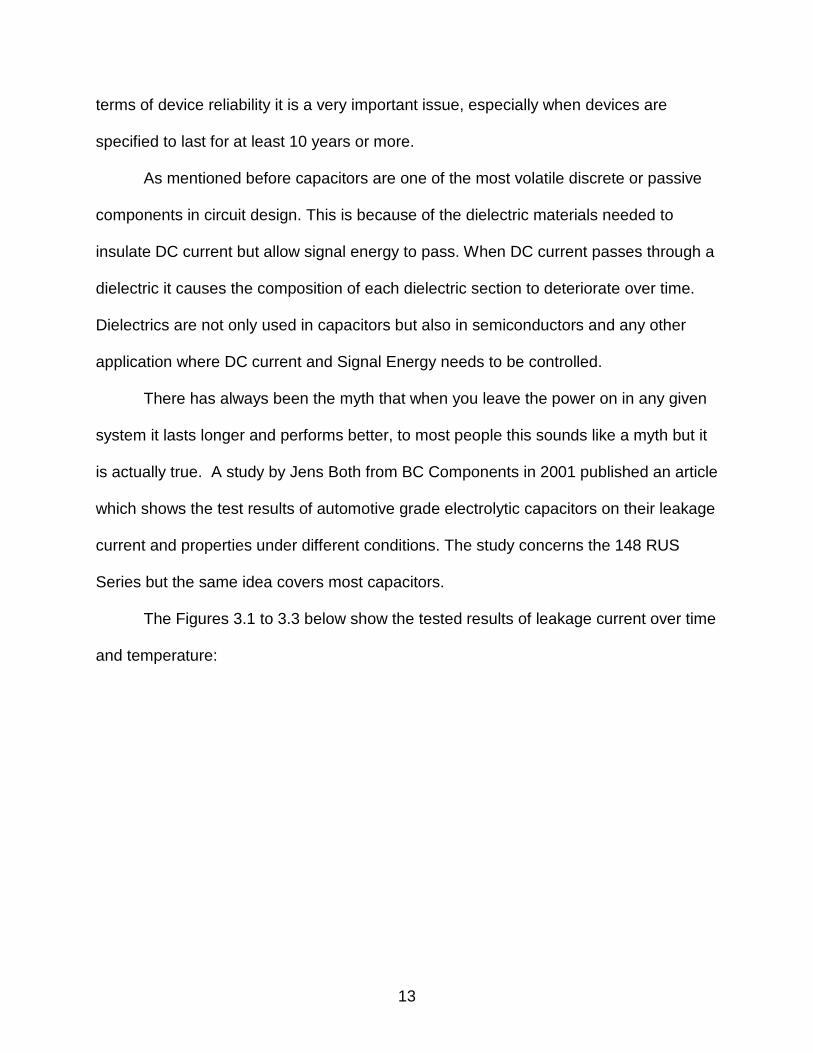
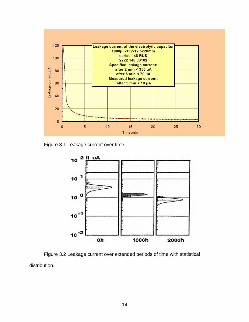
is actually true. A study by Jens Both from BC Components in 2001 published an article
which shows the test results of automotive grade electrolytic capacitors on their leakage
current and properties under different conditions. The study concerns the 148 RUS
Series but the same idea covers most capacitors.
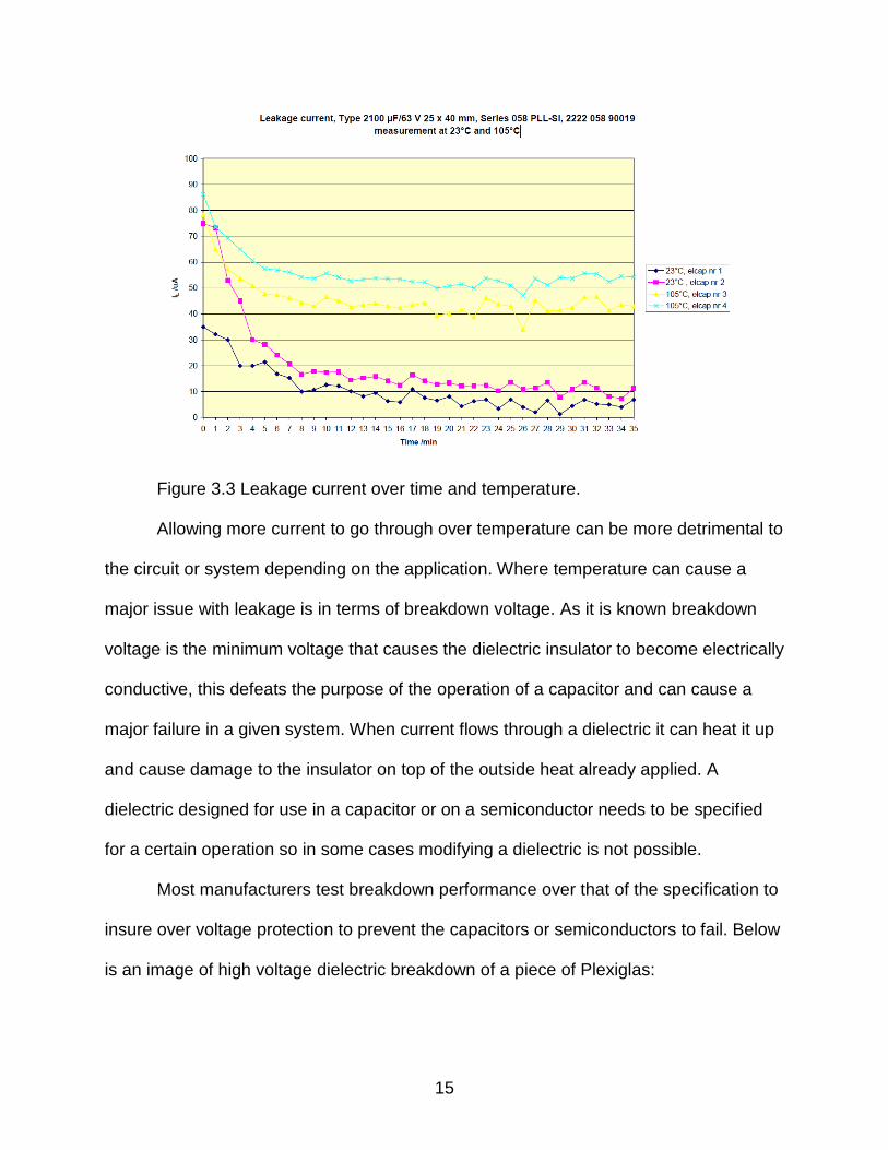
The Figures 3.1 to 3.3 below show the tested results of leakage current over time
and temperature:
13
Page 20
Figure 3.1 Leakage current over time.
Figure 3.2 Leakage current over extended periods of time with statistical
distribution.
14
Page 21
Figure 3.3 Leakage current over time and temperature.
Allowing more current to go through over temperature can be more detrimental to
the circuit or system depending on the application. Where temperature can cause a
major issue with leakage is in terms of breakdown voltage. As it is known breakdown
voltage is the minimum voltage that causes the dielectric insulator to become electrically
conductive, this defeats the purpose of the operation of a capacitor and can cause a
major failure in a given system. When current flows through a dielectric it can heat it up
and cause damage to the insulator on top of the outside heat already applied. A
dielectric designed for use in a capacitor or on a semiconductor needs to be specified
for a certain operation so in some cases modifying a dielectric is not possible.
Most manufacturers test breakdown performance over that of the specification to
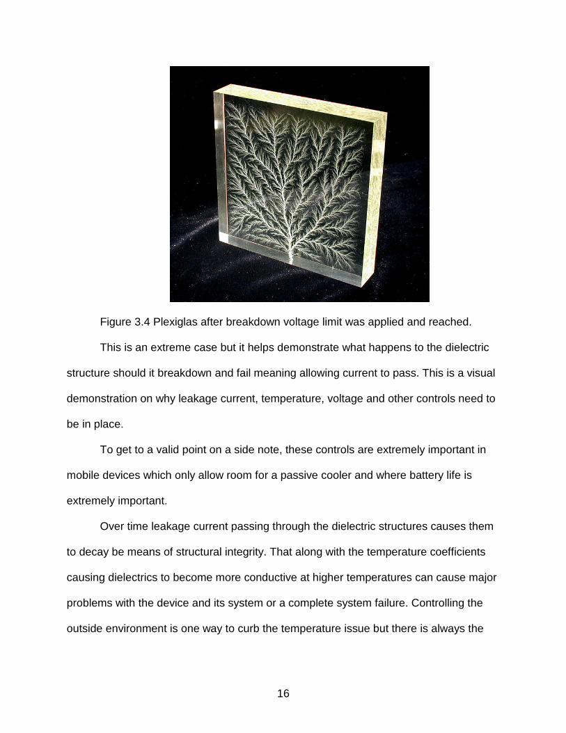
insure over voltage protection to prevent the capacitors or semiconductors to fail. Below
is an image of high voltage dielectric breakdown of a piece of Plexiglas:
15
Page 22
Figure 3.4 Plexiglas after breakdown voltage limit was applied and reached.
This is an extreme case but it helps demonstrate what happens to the dielectric
structure should it breakdown and fail meaning allowing current to pass. This is a visual
demonstration on why leakage current, temperature, voltage and other controls need to
be in place.
To get to a valid point on a side note, these controls are extremely important in
mobile devices which only allow room for a passive cooler and where battery life is
extremely important.
Over time leakage current passing through the dielectric structures causes them
to decay be means of structural integrity. That along with the temperature coefficients
causing dielectrics to become more conductive at higher temperatures can cause major
problems with the device and its system or a complete system failure. Controlling the
outside environment is one way to curb the temperature issue but there is always the
16
Page 23
actual temperature of any given component and in a sealed imbedded system like a
smart phone these issues must be accounted for.
As it is commonly known when any material is repeatedly heated and cooled its
structure decays. This along with voltage applied can further weaken any capacitor.
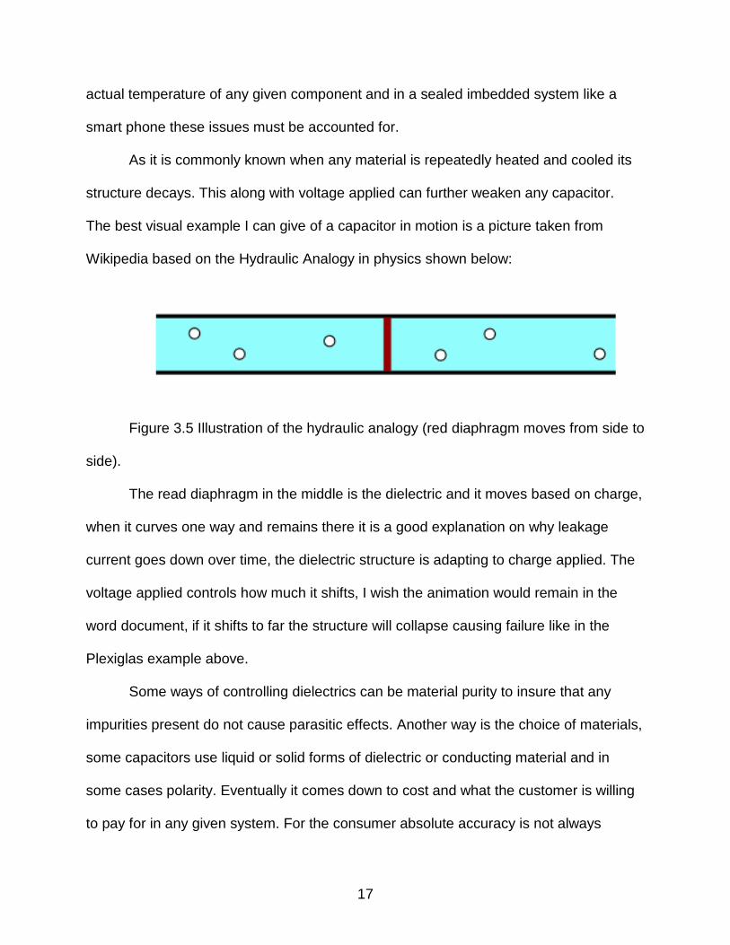
The best visual example I can give of a capacitor in motion is a picture taken from
Wikipedia based on the Hydraulic Analogy in physics shown below:
Figure 3.5 Illustration of the hydraulic analogy (red diaphragm moves from side to
side).
The read diaphragm in the middle is the dielectric and it moves based on charge,
when it curves one way and remains there it is a good explanation on why leakage
current goes down over time, the dielectric structure is adapting to charge applied. The
voltage applied controls how much it shifts, I wish the animation would remain in the
word document, if it shifts to far the structure will collapse causing failure like in the
Plexiglas example above.
Some ways of controlling dielectrics can be material purity to insure that any
impurities present do not cause parasitic effects. Another way is the choice of materials,
some capacitors use liquid or solid forms of dielectric or conducting material and in
some cases polarity. Eventually it comes down to cost and what the customer is willing
to pay for in any given system. For the consumer absolute accuracy is not always
17
Page 24
required and the life expectancy for a consumer device can be 5 years in contrast to
corporate or government usage where they want a 20 year or more life span. This is
where cost and choice of materials can be an issue.
Signal noise is a major issue in both wired and wireless technology, this is why
many capacitors, inductors, etc are used for input and output circuits. As stated above it
is important to have controls on the components and devices itself but how do you
make it where you can accept a wide frequency range? In a lot of circuit designs I have
seen over the years there are usually 5-10 capacitors, and in some cases a few
inductors, in use to filter out unwanted frequency ranges. They are usually different
capacitor values attached from the input or output line in parallel to ground to reject
higher frequencies.
Why reject higher frequencies? In the case of signal noise, when noise is
introduced into the signal for various known reasons, and some unknown, they are
usually much higher frequencies introduced to the desired frequency and as stated
before capacitors allow for passing of higher frequencies. Depending on the application
signal noise can cause a lot of error to an application and in the case of today’s high
speed data requirements it can be a major issue.
18
Page 25
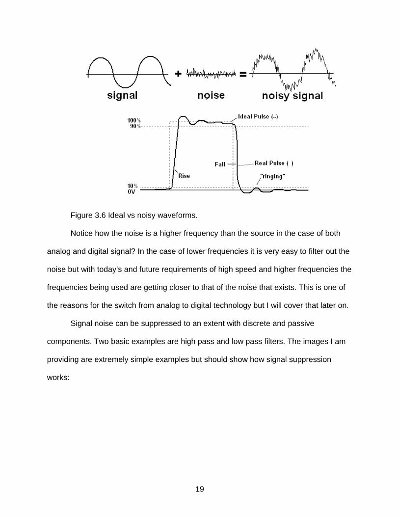
Figure 3.6 Ideal vs noisy waveforms.
Notice how the noise is a higher frequency than the source in the case of both
analog and digital signal? In the case of lower frequencies it is very easy to filter out the
noise but with today’s and future requirements of high speed and higher frequencies the
frequencies being used are getting closer to that of the noise that exists. This is one of
the reasons for the switch from analog to digital technology but I will cover that later on.
Signal noise can be suppressed to an extent with discrete and passive
components. Two basic examples are high pass and low pass filters. The images I am
providing are extremely simple examples but should show how signal suppression
works:
19
Page 26
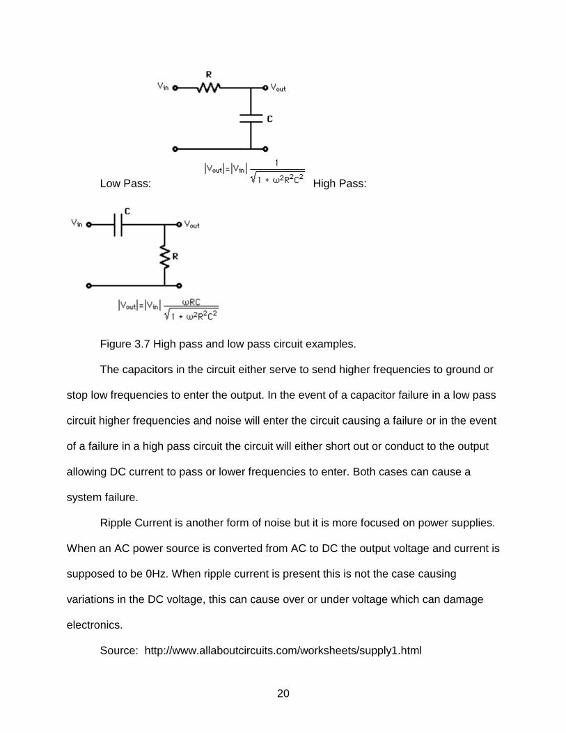
Low Pass: High Pass:
Figure 3.7 High pass and low pass circuit examples.
The capacitors in the circuit either serve to send higher frequencies to ground or
stop low frequencies to enter the output. In the event of a capacitor failure in a low pass
circuit higher frequencies and noise will enter the circuit causing a failure or in the event
of a failure in a high pass circuit the circuit will either short out or conduct to the output
allowing DC current to pass or lower frequencies to enter. Both cases can cause a
system failure.
Ripple Current is another form of noise but it is more focused on power supplies.
When an AC power source is converted from AC to DC the output voltage and current is
supposed to be 0Hz. When ripple current is present this is not the case causing
variations in the DC voltage, this can cause over or under voltage which can damage
electronics.
Source: http://www.allaboutcircuits.com/worksheets/supply1.html
20
Page 27
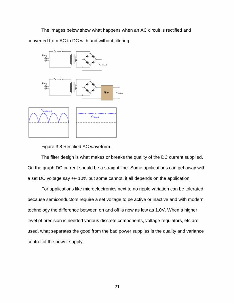
The images below show what happens when an AC circuit is rectified and
converted from AC to DC with and without filtering:
Figure 3.8 Rectified AC waveform.
The filter design is what makes or breaks the quality of the DC current supplied.
On the graph DC current should be a straight line. Some applications can get away with
a set DC voltage say +/- 10% but some cannot, it all depends on the application.
For applications like microelectronics next to no ripple variation can be tolerated
because semiconductors require a set voltage to be active or inactive and with modern
technology the difference between on and off is now as low as 1.0V. When a higher
level of precision is needed various discrete components, voltage regulators, etc are
used, what separates the good from the bad power supplies is the quality and variance
control of the power supply.
21
Page 28
CHAPTER 4
COMPONENT RELIABILITY
Reliability falls under the realm of Quality Control, the question is how do you
make a device more reliable or guarantee a lifespan? This usually falls under production
engineering once a design of a new component or device is complete. A design in itself
may work under simulation or controlled circumstances but it does not necessarily work
as intended out in the field for the intended customer.
In terms of hard data most companies or other agencies will not release any of
their important testing or re-design results and consider anything that gives them the
edge over their competitors a trade secret and protect it under law. It is not difficult to
figure out how a device or component works but it is not easy to figure out how a
manufacturer made it possible. The only thing that can be explained from the outside in
a research capacity is explaining methods to help increase lifespan, specification
control, and reliability.
The first step in component quality is the choice of materials. As stated before I
chose copper wire and carbon resistors to show temperature coefficients but those
materials are not always desired for every application. The reason why I chose them is
because they are common and inexpensive. That leads to the next question, why not
choose the best material for everything? This is because the best materials may cost
more than the customer is willing to pay and may have parasitic properties under certain
circumstances. The price for any material will change over time, increased demand or a
shortage can cause increased prices.
22
Page 29
The choice of materials for wires in the electricity and electronics realm is
basically common sense but I want to take some common examples of the known best
conductors to explain why someone would choose one over the other.
As far as resistors go every manufacturer has a specified resistance level,
resistance variance (tolerance), and wattage. Most modern electronics are run on a
printed circuit board PCB and therefore require a small resistor is needed in the design
hence chip resistors are used. By way of design the best way to help insure that a
resistor does not fail is by not exceeding 50% of the rated wattage. Why not use a
device at its max rated wattage? Because running any electronic device at max capacity
will shorten its life span by either a material breakdown or degradation of material
structure. Manufacturers over watt the device at test to guarantee safety, drift, and life
testing for any given component or device but just because it can pass a test doesn’t
mean that it should be used at max levels at all times. Also various studies have shown
from power supplies, discrete components, etc that electronics in general has peak
efficiency at 50% load.
Most chip resistors use thick film, thin film, or resistance chains inside the chip
package, the name alone can give an idea what they might be used for. In a published
article by Panasonic, a known manufacturer http://industrial.panasonic.com/www-
data/pdf/AOA0000/AOA0000PE36.pdf (found here), they explain some uses of their
resistors and methods of attempting to force a failure and shorten its lifespan.
Application of thin film resistors is more widely used in electronic systems, this is
because they present less noise and can provide higher accuracy. Thick film resistors
are more used in power supply applications. This is because they can allow a higher
23
Page 30
amount of wattage to pass and can be used for low resistance levels. Chain resistors
are a bit harder to explain because chain resistors are used in a network inside the
package either in series, parallel, or both.
The choice of resistor depends on application but in the realm of electronics
(excluding power supplies) thin film is the most ideal. In all the failure scenarios
presented in the article the thin films resistors have an end result of an open circuit, this
is important because if designed correctly an open point in the circuit will cause the
system to stop and shut down. In the case of thick film an open circuit is not the only
failure scenarios create an open situation making predicting reliability very difficult. The
resistance value of thick film resistors can change with overvolting or a large enough
surge in power. A change in resistance value can cause a major failure in a system
because any given design is dependent on knowing the possible range of all
components used for resistance, noise, and power rating. When an overvolt or overwatt
situation occurs it is unknown on what the specification of a thick film resistor will be.
That and allowing current to pass can cause degradation to any given system. The
study is focusing on electronics so I will focus on thin film resistors
The choice of materials is another way to insure component reliability and
accuracy. In the case of thin film resistors Nichrome (NiCr), which is about 80% nickel
and 20% Chromium, is a common material used. Nichrome is commonly used due to its
reliability, low noise, easy control, and relatively low cost. Accuracy is controlled in a few
forms, as described earlier temperature can affect resistance values, Nichrome has a
coefficient of 0.0004 on average in pure material form. As we know insulators have a
negative temperature coefficient and conductors have a positive one. Nichrome has
24
Page 31
been widely used for over 100 years because of its properties of temperature stability
and oxidation resistance, this makes it an ideal choice for use in electronics.
For a 50Ohm Nichrome Resistor at 20C, the resistance at 85C would be
51.3Ohms, that’s a 2.6% variance, which doesn’t seem like much but in
microelectronics it can be a lot. Another way is to cut the resistor to a desired value, this
can be done by laser trimming, by micro machining the resistor to value, or by controlled
depositing of the material.
A second material worth mentioning is Sichrome (SiCr), this material is less
documented because these resistors are usually made on a wafer through material
deposition. There is little data about SiCr because every manufactuer has a different
method of making the resistors and have multiple patents concerning it. The TCR of
Sichrome is roughly -0.0004, in combination with Nichrome in a chain formation this can
make an ideal situation with offsetting temperature coefficients. This is commonly done
with semiconductors and discrete components made through wafer processing or other
silicon manufacturing methods.
Since a wafer is pure silicon, chromium can be introduced to it to create SiCr.
Through manufacturing methods the TCR, size, resistance level, etc can be easily
controlled. One example would be:
US Patent: US 6171922 B1, found here: http://www.google.com/patents/US6171922,
published in 2001 and filed by National Semiconductor. This explains a process of
controlling the TCR through wafer fabrication processing. There are many other patents
out there like it, since SiCr can be made through chemical deposition many companies
and organizations do not reveal the data of SiCr resistors. There are few physical tables
25
Page 32
out there about it because it can be varied by process control, the idea is to either keep
it close to 0 or use it to offset the TCR of all other materials used.
Resistor manufacturing is a challenge in itself but it is easier to control than other
components. Size, material purity, material choice, material behavior, and process
technique are even more critical when it comes to capacitors.
In semiconductors and microelectronics, resistors and capacitors are the most
commonly used discrete components, especially inside an IC. Diodes, transistors, etc
are also main building blocks but I will be getting to those soon.
There are three commonly used capacitor types used in electronics: ceramic,
film, and electrolytic. Ceramic and film capacitors are generally non-polarized and
easier to produce, both of these are solid materials and are easier to manufacture and
control. Electrolytic capacitors can come in solid and non-solid form, the capacitors are
desired in cases where polarity is needed and where a high capacitance level is
needed. The picture below shows the capacitance and voltage where types of
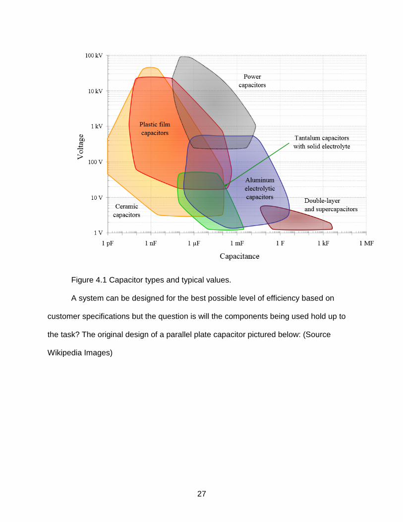
capacitors are needed: (Source: Wikipedia Images)
26
Page 33
Figure 4.1 Capacitor types and typical values.
A system can be designed for the best possible level of efficiency based on
customer specifications but the question is will the components being used hold up to
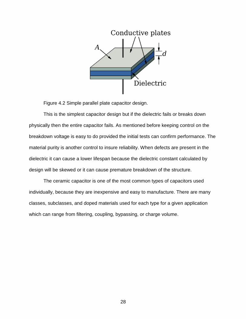
the task? The original design of a parallel plate capacitor pictured below: (Source
Wikipedia Images)
27
Page 34
Figure 4.2 Simple parallel plate capacitor design.
This is the simplest capacitor design but if the dielectric fails or breaks down
physically then the entire capacitor fails. As mentioned before keeping control on the
breakdown voltage is easy to do provided the initial tests can confirm performance. The
material purity is another control to insure reliability. When defects are present in the
dielectric it can cause a lower lifespan because the dielectric constant calculated by
design will be skewed or it can cause premature breakdown of the structure.
The ceramic capacitor is one of the most common types of capacitors used
individually, because they are inexpensive and easy to manufacture. There are many
classes, subclasses, and doped materials used for each type for a given application
which can range from filtering, coupling, bypassing, or charge volume.
28
Page 35
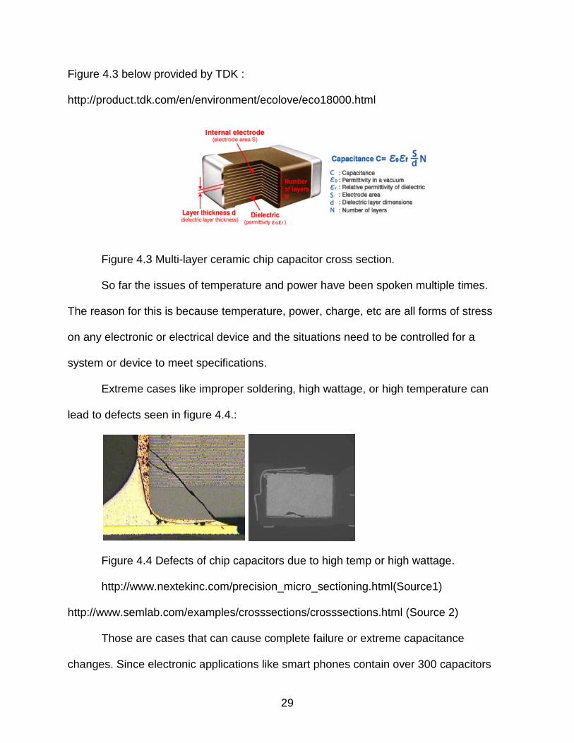
Figure 4.3 below provided by TDK :
http://product.tdk.com/en/environment/ecolove/eco18000.html
Figure 4.3 Multi-layer ceramic chip capacitor cross section.
So far the issues of temperature and power have been spoken multiple times.
The reason for this is because temperature, power, charge, etc are all forms of stress
on any electronic or electrical device and the situations need to be controlled for a
system or device to meet specifications.
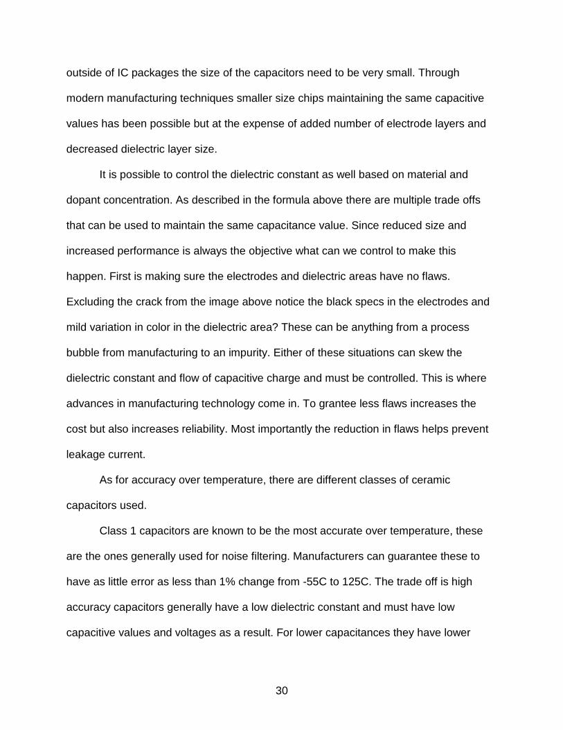
Extreme cases like improper soldering, high wattage, or high temperature can
lead to defects seen in figure 4.4.:
Figure 4.4 Defects of chip capacitors due to high temp or high wattage.
http://www.nextekinc.com/precision_micro_sectioning.html(Source1)
http://www.semlab.com/examples/crosssections/crosssections.html (Source 2)
Those are cases that can cause complete failure or extreme capacitance
changes. Since electronic applications like smart phones contain over 300 capacitors
29
Page 36
outside of IC packages the size of the capacitors need to be very small. Through
modern manufacturing techniques smaller size chips maintaining the same capacitive
values has been possible but at the expense of added number of electrode layers and
decreased dielectric layer size.
It is possible to control the dielectric constant as well based on material and
dopant concentration. As described in the formula above there are multiple trade offs
that can be used to maintain the same capacitance value. Since reduced size and
increased performance is always the objective what can we control to make this
happen. First is making sure the electrodes and dielectric areas have no flaws.
Excluding the crack from the image above notice the black specs in the electrodes and
mild variation in color in the dielectric area? These can be anything from a process
bubble from manufacturing to an impurity. Either of these situations can skew the
dielectric constant and flow of capacitive charge and must be controlled. This is where
advances in manufacturing technology come in. To grantee less flaws increases the
cost but also increases reliability. Most importantly the reduction in flaws helps prevent
leakage current.
As for accuracy over temperature, there are different classes of ceramic
capacitors used.
Class 1 capacitors are known to be the most accurate over temperature, these
are the ones generally used for noise filtering. Manufacturers can guarantee these to
have as little error as less than 1% change from -55C to 125C. The trade off is high
accuracy capacitors generally have a low dielectric constant and must have low
capacitive values and voltages as a result. For lower capacitances they have lower
30
Page 37
impedances at much higher frequencies so for high speed and frequency applications
these are an ideal choice. For low frequency and high voltage applications the opposite
is true, this is where class 2 MLCC’s come in. Though they cannot maintain the same
accuracy over the same range they can maintain between 10-15% accuracy over the
same temperature range and have a higher dielectric constant, making them easier to
manufacture and cheaper for the customer. The choice of which to use when is up to
the designer.
Film capacitors are another type, where these are important is that they not only
exist in exterior packages but are also used in fabrication on IC chips if a capacitor is
needed inside the package.
A bit of feed forward, IC chips generally have transistors, diodes, film capacitors,
and film resistors inside the package. This can be done because in wafer processing
multiple layers of metal conductors, dielectrics, and doped silicon are used and those
devices can be created on wafer easily if needed on the IC. Inductors, relays, polarized
electrolytic capacitors etc are generally placed outside the package because of the
practicality and properties of their use. Research is being done this day to print
inductors in an IC and package and relays in an IC via MEMS but these are still in
infancy and are possible now but expensive and hard to come by.
Film capacitors are known for their high levels of accuracy both in tolerance and
over temp. Tolerance can be achieved by means of wafer fabrication, laser trimming, or
processing techniques. Like Class 1 capacitors they usually maintain a low dielectric
constant and have lower capacitance values.
31
Page 38
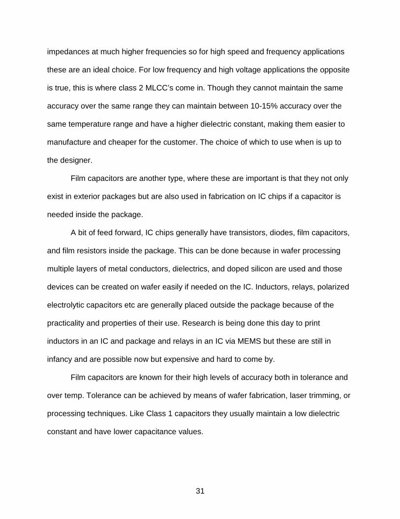
Where attention is usually paid in terms of reliability is in electrolytic capacitors.
As the name presents the dielectric is a liquid electrolyte. These capacitors are known
to have the largest drift over temperature, highest current leakage, and high variance in
capacitive value. Where these capacitors are highly needed is in applications that
require high capacitance values and polarity, usually power supplies, high signal
energy, and points where the polarity of the charge is important. There are other
designs in the mix that do not use a liquid dielectric for the same purpose but they are a
work in progress since they cannot yet match the performance or capacitance of
electrolytics.
Figure 4.5 Internal components of an electrolytic capacitor. Source: (Wikipedia
images)
32
Page 39
Where the reliability of a capacitor matters the most is in the dielectric, over time
the liquid will breakdown in its electrical properties. Controlling temperature is a must for
these, if the temperature gets too low major current leakage will occur, the liquid will
contract causing the encasement to fail (seal break), the aluminum foil can break, or the
capacitor will completely shut down. In cases of high temperature the liquid will
evaporate causing a possible point of conduction (short), the fluid will expand enough to
break the seal of the case, or complete failure of the component. An excessive amount
of current, voltage, or wattage can also cause the high temperature fails even if there is
temperature control. These capacitors have the shortest lifespan due to usage and the
nature of the materials.
The process behind the aluminum fail is also very important. Usually the fail is
roughed up on the inside a certain way (manufacturers will not reveal how) before the
liquid and paper are inserted, this is to give the charge a direction and control the flow of
the charge between the anode and cathode foil.
A reliability article published by Panasonic here:
http://industrial.panasonic.com/www-data/pdf/ABA0000/ABA0000TE4.pdf shows
various failure modes.
Multiple manufacturers and studies have shows that the ideal temperature for
electrolytic capacitors to run is at 40C (104F) this is because it is the optimal
temperature for the electrolytic fluids to pass a charge, control leakage, and maintain
stability. When current runs through any device it will heat up so keeping the capacitors
at room temperature is not practical, In terms of cooling it is much easier to cool to 40C
than 23C.
33
Page 40
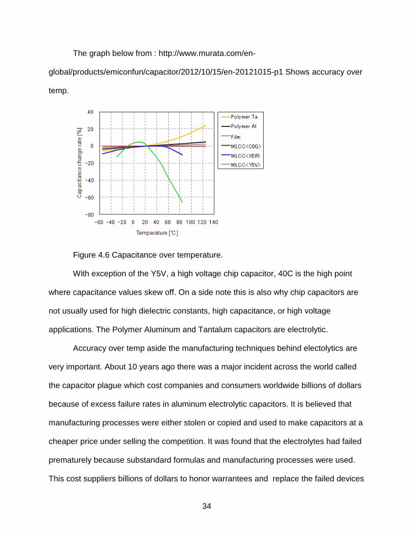
The graph below from : http://www.murata.com/en-
global/products/emiconfun/capacitor/2012/10/15/en-20121015-p1 Shows accuracy over
temp.
Figure 4.6 Capacitance over temperature.
With exception of the Y5V, a high voltage chip capacitor, 40C is the high point
where capacitance values skew off. On a side note this is also why chip capacitors are
not usually used for high dielectric constants, high capacitance, or high voltage
applications. The Polymer Aluminum and Tantalum capacitors are electrolytic.
Accuracy over temp aside the manufacturing techniques behind electolytics are
very important. About 10 years ago there was a major incident across the world called
the capacitor plague which cost companies and consumers worldwide billions of dollars
because of excess failure rates in aluminum electrolytic capacitors. It is believed that
manufacturing processes were either stolen or copied and used to make capacitors at a
cheaper price under selling the competition. It was found that the electrolytes had failed
prematurely because substandard formulas and manufacturing processes were used.
This cost suppliers billions of dollars to honor warrantees and replace the failed devices
34
Page 41
and systems to their customers. The formula for the electrolytes and the foil is a very
closely guarded trade secret it is not as easy as copying a method to create a reliable
component.
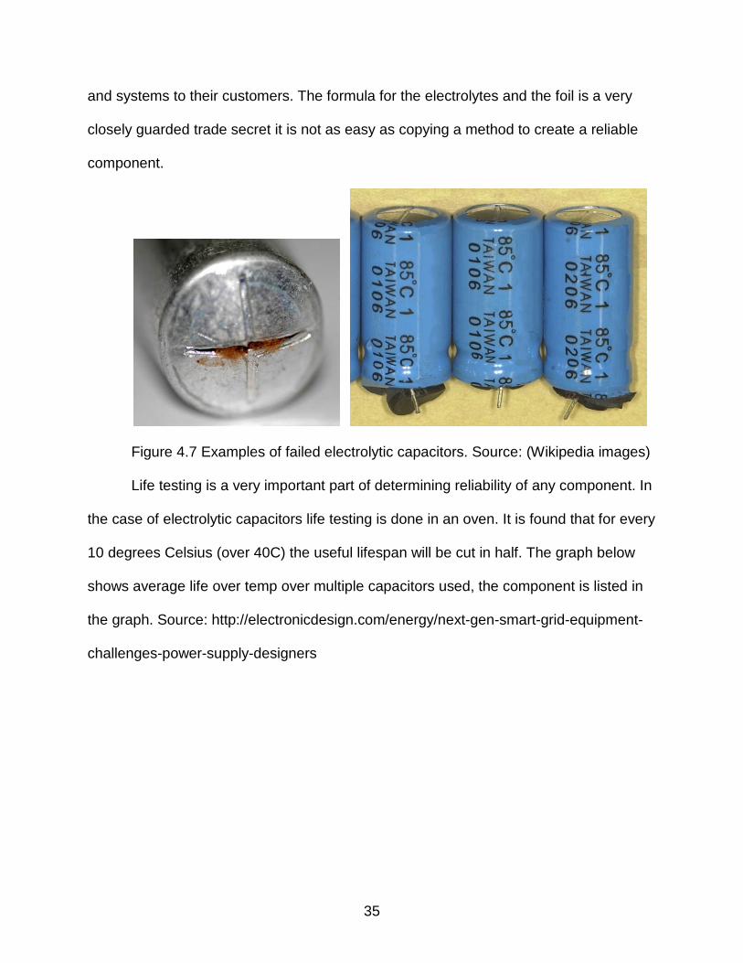
Figure 4.7 Examples of failed electrolytic capacitors. Source: (Wikipedia images)
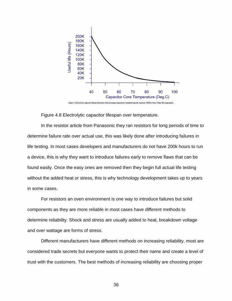
Life testing is a very important part of determining reliability of any component. In
the case of electrolytic capacitors life testing is done in an oven. It is found that for every
10 degrees Celsius (over 40C) the useful lifespan will be cut in half. The graph below
shows average life over temp over multiple capacitors used, the component is listed in
the graph. Source: http://electronicdesign.com/energy/next-gen-smart-grid-equipment-
challenges-power-supply-designers
35
Page 42
Figure 4.8 Electrolytic capacitor lifespan over temperature.
In the resistor article from Panasonic they ran resistors for long periods of time to
determine failure rate over actual use, this was likely done after introducing failures in
life testing. In most cases developers and manufacturers do not have 200k hours to run
a device, this is why they want to introduce failures early to remove flaws that can be
found easily. Once the easy ones are removed then they begin full actual life testing
without the added heat or stress, this is why technology development takes up to years
in some cases.
For resistors an oven environment is one way to introduce failures but solid
components as they are more reliable in most cases have different methods to
determine reliability. Shock and stress are usually added to heat, breakdown voltage
and over wattage are forms of stress.
Different manufacturers have different methods on increasing reliability, most are
considered trade secrets but everyone wants to protect their name and create a level of
trust with the customers. The best methods of increasing reliability are choosing proper
36
Page 43
materials, proper design, and high levels of quality control by introducing failures and
correcting the errors, none of these are cheap. As none of these are highly discussed in
the classroom or a design environment reliability is very important to a company and the
customer and is a major field in the realm of engineering, even at the level of discrete
components.
37
Page 44
CHAPTER 5
MATERIALS USED IN SEMICONDUCTORS
In the process of semiconductor manufacturing the most common base material
used is Silicon (Si), there are multiple reasons why. The first reason for this that it is in
the (IV) fourth element group and it is in the middle ground of being either an insulator
or conductor. This makes it an ideal candidate for semiconductor usage. By itself it
does not act as a conductor or insulator until it is mixed, or doped with the correct
materials. It is also the most desired material because it is commonly found, exists
naturally, maintains a solid element structure, oxidizes naturally, and is the cheapest to
produce. What is used is a refined version of the pure element, the silicon used in
semiconductors is extracted from sand and other silicate deposits found on the earth.
To make silicon work as a semiconductor it has to be doped with other materials to
pass a charge. Boron and phosphorus are two common materials used, they come
from the III and V valence groups respectively and make use of silicon’s electrical band
gap to pass a charge.
Gallium arsenide (GaAs) is the second most commonly used base
semiconductor material, it is known as a III-V compound material according to its points
on the periodic table of elements. GaAs offers a few advantages over silicon which
make it desirable in some cases. The first is that it has a much higher electron mobility
than silicon which allows for very high switching speeds and can function at frequencies
well over 250GHz. GaAs is also not as sensitive to heat as silicon is, this allows it to
operate at temperature ranges outside that of common silicon devices helping to
improve device reliability in certain cases.
38
Page 45
As there is much more information about the materials used in semiconductors I
would like to get into what can cause non-ideal effects that have to be accounted for in
designing semiconductor devices for improved reliability and or non-ideal conditions.
Ohm’s law as we all know is one of the most basic laws in any realm of electronics
whether it be electrical, electronic, or in any other form. As heat and pressure go up so
does resistance and since a semiconductor device has an output function based on
either input voltage or current the desired affect can be altered by a change in
resistance.
Semiconductor device physics act differently than basic electronics but the idea
of a change in resistance remains the same under non-ideal operating conditions.
Electron mobility is how quickly an electron can move which directly affects device
performance. This is one of the measurements used in semiconductor design and
determines semiconductor device capability.
Since a semiconductor is what it says it is made of resistive materials which lean
either toward an insulator or conductor, meaning all materials are essentially resistive.
Doping and Ion Implantation introduce certain materials which direct the flow of
electrons to reach the desired switching operations. Boron as a p-type and Phosphorus
as an n-type, among a few examples, can be introduced to create a desired operation.
N-type transistors are known for a higher device mobility but in many cases P-type
transistors are needed to complement the N-types for many applications including
digital logic and other push-pull networks. This requires a worst case scenario in design
to compensate for the P-type mobility rating.
39
Page 46
On top of implanting P and N type materials for transistor structure thin film
resistors are also added into many designs for any given purpose. These resistors are
doped material as well but act more like a conventional resistor. The doping or
implanting concentration also is a factor in device mobility, more isn’t always better in
most cases but to compensate for device reliability and consistent accuracy in the
specified operating range a desired target value needs to be found for the material
concentration. Expanding and contacting of materials over temperature happen at the
atomic level thus altering the device characteristics, resistance, and electron mobility.
Higher concentrations of materials can lead to less mobility due to the lack of electrons
or electron holes and the same is true in reverse so a balance has to be applied in any
design case. I will go further into detail later in the report.
The insulating layer which is grown either with a natural silicon oxide, or with an
artificial insulating layer which is the case with most other semiconductor materials and
in some cases silicon, has an effect on how the device runs. Dielectrics also play a part
in some devices for many of them block the flow of DC current. If the insulating layers or
dielectrics are not in proper order then current leakage can occur. Recently since digital
manufacturers have been producing lithography sizes lower then 65nm it has become a
major issue. This is because at that size the insulating layers are only a few atoms thick.
Current leakage can affect the potential gain for any transistor based device, because
theoretically an ideal device has no current entering or leaving the op-amps or other
devices in use inside of an IC, but the real world is not ideal. Since an already accepted
amount of leakage happens it has to be controlled, this is why the insulating layers or
40
Page 47
dielectrics are so important. When temperature increases so does the current leakage,
this is one of many paracitic effects that must be accounted for in design.
When it comes to design and intent for use the purpose of the device must be
established. In terms of operating temperature and other device specifications. The
consumer operating range is generally from 0C to 85C, in most cases narrower than
that, where say the military standard (that we know of) is usually between -55C and
125C and military spec expects the range to be guaranteed for worst case scenarios.
The difference in temp for consumer range is 85C and in many cases lower than that, I
am choosing consumer and military since they are the two common operating ranges
that have the greatest difference. The narrower spec is easier to work with and design
for which is why consumer grade parts are cheaper, where the military grade parts have
a range of 180C and must be guaranteed. That is over double and in some cases triple
the range that a part is expected to perform to its guaranteed specification, I haven’t
even touched ranges outside of that yet.
The band gap of all materials used on a device after it is finished has a lot to do
with its performance range. Band gap is usually associated more with solid state
physics than with electronics but I will give the brief version of it for now. Silicon has a
band gap of 1.1 eV (electron volts) where Gallium Arsenide has a gap of 1.4 eV. This is
the material difference between the valence and conduction band of the material. That
0.3eV actually makes a big difference, it not only allows GaAs to run at 100x the
frequency with the same amount of heat but GaAs is less sensitive to thermal effects
than Si is. Conductors have a lower band gap where insulators have one that is much
higher, semiconductors range from 0.6 to 4.0eV roughly. A band gap has to exist for a
41
Page 48
switching operation to take place which is what an IC device usually does. As far as
which one is ideal there is no one answer but for extreme temperature devices, i.e. drill
bit sensors or satellite IC’s. A band gap of 1.7eV or higher is desired for extremely high
temperatures or devices that require a very large operating range, there are a few
choices to choose from in this range but it is not commonly revealed which ones are
used for which application.
Aside from the choice of the material itself, Si actually has a wide range of
applications; some manufacturers prefer a more expensive component to insure higher
quality or some have a process capable of refining a common material well enough to
provide the same results for less cost. There are many factors which can insure a more
reliable part that does not require a material change. For some device designs the
difference between a consumer part and military part is a matter of material purity,
device packaging, environmental isolation, and picking the parts that test closest to the
middle of the device specification, a process called binning which I will describe along
the way. I can also include other factors like humidify, pressure, and shock into the
equation, which I will, but I am starting with temperature since it is the most prevalent in
any environment and directly or indirectly affects the other factors.
As stated before where material choice, doping, and the concentration can affect
electron mobility this is a best case scenario. Parasitic sub particles and contamination
also contribute to the degradation of electron mobility. You can always have a group of
chips at test with dead center response but if any forms of contamination or other device
flaws are present it can cause problems further down the road. One thing about
manufacturing is that it always has to be done in hopes of making a profit. Every
42
Page 49
manufacturer wants to make the best parts on the market with zero impurities and have
peak efficiency, some get close to that consistently. However the average consumer is
always on a budget where the military is part of the government and money is less of an
object for them and they have more of it (Politics aside). In the case of manufacturing, to
guarantee that parts meet much tougher requirements the cost goes up.
In most automotive, military, or extreme industrial applications a devices
reliability can be the difference between a satisfied customer or a major failure that has
safety risks. This is why some customers demand zero defects and perfect reliability
over a very wide operating range. What makes high standards so expensive is that
there are always defects and chips that do not perform to said standards. From sawing
the ingot to final chip packaging maybe one in every ten devices at every processing
point meet the requirements. On top of that more qualified individuals are required to
work on and inspect each processing point further driving the cost up where before
some of those points did not require as much attention.
Packaging of the device can also play a major factor in device reliability and
performance. The majority of devices seen in the market have plastic molding around
the chip, this is because it is the cheapest form of packaging and the majority of
consumer use will never need anything beyond that. For heavy environmental
conditions a ceramic package may be required. The advantage to a ceramic package is
that it is capable of dissipating heat better and can be hermetically sealed to prevent
moisture or anything else from entering and affecting the die. When die age or go under
stress the protective nitride layer on top of the die can deteriorate or crack, allowing
moisture or air to touch the components of the die. When this happens the oxidation on
43
Page 50
the die will continue to expand again thus altering the resistance and overall device
performance. This is one of many reasons to understand what a device is going to be
used for or its requirements. A sealed package can keep outside interference out and
being ceramic will protect it more and help dissipate heat but ceramic casing is not
cheap and the seal also has to be tested which will lead to more chips failing a specific
test in line where plastic is cheaper, faster, doesn’t require further reliability testing
beyond the electrical device test.
Another common packaging method to control device conditions is that seen on
computer CPU’s to have active or passive cooling through a metal heat dissipater.
These methods are usually required on CPU’s and other devices that either have a
large amount of transistors, a very fast switching operation, or devices that run a high
amount of current through them.
44
Page 51
CHAPTER 6
DIGITAL TECHNOLOGY
Digital technology is the process if calculating discrete numbers in the form of
voltage levels or in any other form of a discrete number. The technology and the idea
has been around for many years, Morse code is an example, but became very popular
in the 1980’s and especially the 1990’s. It was around that time frame where discrete
voltage levels in the form of a binary 1 or 0 were able to be calculated fast enough on a
semiconductor device to produce results to rival and in some cases surpass previously
used analog technology.
The factors involved in the emergence of digital technology were cost, reliability,
and repeatability. Cost is always a factor in any form of technology. When the transistor
was first invented they were very expensive. Factor in all the transistors required to
make the logic gates and all the logic gates required to do simple addition and
subtraction the cost built up very fast. This is why digital technology did not take off right
away.
Repeatability was one of the primary reasons why digital technology was desired
for multiple applications. Over time the condition of any device will degrade, especially if
used enough. Since analog technology was based on precision values degradation was
a major issue. When used in a wireless application any noise from point to point can
always cause degradation, which there always is when transmitting over the air. The
most common form of storage for analog at the time was magnetic tapes in one form or
another. When used enough either being read, written, or re-written the tape would
wear or the metallic substance would fade causing degradation in the data stored.
45
Page 52
If you can remember large stereo amps with a large amount of capacitors and
inductors, over the air TV transmissions prior to 2009, and VHS tapes you can
remember how degraded the video and audio quality was from either being used over
time or received over a long distance. This is where digital technology offers a solution.
Digital signal processing is the modern solution for the old analog filters. Where
signal filters used to be a combination of various components, now lines of code can be
written to filter undesired noise out of a received signal. This is first done by sampling an
analog signal and converting it to discrete levels and from there process through a
digital filter, basically a program meant to simulate the effects of the components
previously used. Since discrete components can wear and decay over time causing
undesirable effects in the precision values required digital filters are a solution for this
problem requiring CPU power using discrete numbers eliminating the need for precision
values.
Reliability was a major factor in the need for digital technology. Since error and
decay as previously mentioned was a major issue with analog technology digital offered
a solution to these issues. Since digital uses numbers represented in binary,
mathematic calculations and computations can be used to compensate for error. Since
the voltage levels required representing either a 1 or 0 do not need to be precise and
grant room for error decay and slip in precision levels do not factor in to digital
technology as much.
A digital signal is really an analog signal shaped to switch from a specified high
or low voltage level instantaneously. The switching speed was a major factor on why
digital technology took decades to become mainstream. Using TTL (Transistor-
46
Page 53
Transistor) Logic as an example a high voltage level representing a 1 can be anywhere
from 2.2 to 5 Volts over a 5 Volt Supply and a low level can be anywhere from 0/GND to
0.8V, this is how the precision value problem was solved.
As digital has replaced analog technology in many forms the technology still
presents multiple issues that must be accounted for in any design. As mentioned
before previous digital technologies used 5 Volts as a supply but that has decreased
over time, now we are using supplies ranging in the 0.9 to 1.2 Volt range. The clock
cycles, switching speeds, and transistor count are the top contributors to power
consumption. Power consumption plays a major role in device reliability from reasons to
structure integrity to device performance.
When the Intel 8086 was first released in 1978 this was considered a major
breakthrough chip as it was the first chip to use the x86 architecture which is still used
today. At the time it was considered top of the line, this chip used a supply voltage of 5
Volts, had a transistor count of 29,000, had a lithography size of 3 um, and had a clock
cycle of 5MHz. Fast forward to today and lets compare to Intel’s core i7-3770, I am
using the Ivy Bridge core i7 made in 2012 because the design is now final where the
Haswell/Broadwell is still not finished in its design process. The core i7-3770 has a
supply voltage of 1.1V, transistor count of 1.4 billion, lithography size of 22nm, and a
clock cycle of 3.4GHz.
Why is this important when it comes to device reliability? Thermal design power
(TDP) is a major factor that can contribute to the lifespan of a CPU and contribute to its
performance or lack thereof. With the previously mentioned CPU’s in mind, power
consumption jumped from 1.5-2 Watts used in the 8086 to 77W used in the i7. What
47
Page 54
makes the TDP even more important is that the 77W required is run through a die that
is 160mm^2, which is roughly about ¼ the size of a postage stamp.
When lithography sizes are reduced more transistors were able to be packed in
the same space as before. Another advantage of this is that the transistors required less
power because with shorter distances from point to point (typically drain to source, etc)
less current was required to move a charge. This is excellent for saving power but
smaller sizes usually mean the feature is less robust, this is where design comes into
play.
The load-strength tradeoff is key to device reliability and device lifespan, I am
using design techniques for a CPU because it is the one component of a computer that
is the most volatile and requires the most attention (Only High end GPU’s can be a
possible exception).
With smaller features comes the potential for more to be placed in the same
area, however smaller features are not capable of as much load as before (using the
same materials and same design concept), this is why in design supply voltage and
current usage must be accounted for. Even though less power is required for a smaller
feature, if more are placed together in the same space previously used heat can build
up faster with more activity. Since the heat buildup from the TDP affects the entire chip
certain trade offs must be recognized.
Clock speed is also a major factor behind TDP, it is the fastest part of the CPU
and sets the intervals of switching for the rest of the CPU. The higher the switching
speed the more overall friction is created within the CPU therefore increasing the load
and overall TDP. Some methods of curbing this was to decrease the supply voltage,
48
Page 55
with the feature sizes decreasing lowering the supply voltage was not a major issue but
did require some compensation via design. Finding an optimal clock speed is also a
way to increase the lifespan by decreasing the load and TDP. In most portable devices
under clocking and under volting the CPU is a popular idea because there is little room
for heat dissipation and in some cases none. Examples of these ideas would be laptops
and smartphones.
About 10 years ago clock speeds kept jumping and power usage was going up
along with it. The feature size and supply voltage did help curb power consumption
and device reliability but around 2006 CPU power consumption was getting near the
100W mark for the desktop PC. The solution to this issue was multi-core CPU
applications. What multi-core does is it has multiple Logical CPU’s on the same die
that share a common clock and can divide the work load between them. The issue is
that the software needs to be written or re-written to make use of the new architecture,
this is the point when 64-bit operating systems and programs came into play.
Even though technology is obsolete in a matter of a few years, or even a few
months, the solution among the consumer population is to replace their CPU or the
entire computer should the CPU fail or if it does not meet their specification needs.
However replacing hardware does not fit the need of everyone, especially governments
and private industry. For some specific applications a specific set of hardware must be
used, this condition usually applies to applications that require absolute reliability and
consistency. Since a specific application must go through rigorous testing to be qualified
to fit a specific need replacing hardware may not be an option, in these cases when a
component fails that same specific component must be replaced, including the CPU.
49
Page 56
Since CPU manufacturers only produce a CPU for a specific period of time customers
usually ask for a stock pile of parts and some guarantee that the part will last for a
specified duration, this is why device reliability and device lifetimes are so important.
50
Page 57
BIBLIOGRAPHY
Panasonic Industrial, Panasonic Corporation, http://na.industrial.panasonic.com/
TDK Industrial, TDK Corporation, http://www.global.tdk.com
Wikimedia commons, http://www.wikipedia.org
All About Circuits, http://www.allaboutcircuits.com
Basic Electronics Tutorials, http://www.electronics-tutorials.ws
Patrick J O’Conner, Practical Reliability Engineering 5th ed.,
John Wiley and Sons, Inc., New York City, NY, 2012
Neil Weste and David Harris, CMOS VLSI Design 4th ed.,
Addison-Wesley, Boston, MA, 2011
John G. Proakis and Dimitris K. Manolakis, Digital Signal Processing 4th ed.,
Prentice Hall, Upper Saddle River, NJ, 2006
Behzad Razavi, Design of Analog CMOS Integrated Circuits,
The McGraw-Hill Companies, Inc., New York City, NY, 2001
David M. Pozar, Microwave Engineering 4th ed.,
John Wiley and Sons, Inc., New York City, NY, 2012
51
Web
Textbooks