17 Laser-Based Determination of Decohesion and Fracture Strength of Interfaces and Solids by Nonlinear Stress Pulses Peter Hess University of Heidelberg Germany 1. Introduction To determine the mechanical strength of films, coatings and solids the loss of adhesion or fracture must be investigated. The failure of interfaces and bulk materials is a dominant issue in microelectronics with multilayer systems and micro-electro-mechanical-system (MEMS), nano-electro-mechanical-system (NEMS) and sensor devices, based essentially on single-crystal silicon as basic material, which is considered here in detail. A versatile tool that is quite often used for strength analysis is the scratch tester, where a diamond stylus is drawn across the coated surface under increasing load to determine the critical load, or the stylus is used as an indenter. These methods are versatile, but besides being influenced by the properties of the system itself they also depend on several test parameters, such as scratching velocity and stylus properties, which affect the critical load. Owing to the complexity of the failure processes involved, in connection with strongly inhomogeneous deformation fields, it is generally very difficult to extract quantitative values of the cohesion or fracture strength (Lacombe, 2006). In fact, the most widely used testing methods, such as peel, pull, scratch, blister, indentation and beam-bending tests, usually involve plastic deformations, which are difficult to analyze (Wei & Hutchinson, 1998). Some of these quasi-static methods do not reach the strength limit of the strongest material systems or require intricate sample preparation. In this review the contact-free measurement of the strength of interfaces and bulk materials will be discussed employing pulsed lasers to launch strongly nonlinear stress pulses. In fact, quantitative information on the failure strength of materials can be obtained by laser-based excitation and detection techniques. Normally a nanosecond laser pulse is used to excite either bulk or surfaces acoustic stress waves, which develop shocks during propagation. In these laser-controlled pump-probe setups a continuous-wave (cw) laser probe is used to measure the transient surface displacement or surface velocity, providing the information on the elastic stresses achieved. The laser techniques are contact-free and normally need no artificial seed crack to induce failure because stresses of 5-10 GPa can be attained in the elastic shock pulses generated. For studying interfacial strengths usually bulk acoustic waves are used. With a laser pulse a one-dimensional (1D) compressive longitudinal wave packet is launched in a thin metal film covering the back side of the substrate. The critical failure stress of the film/substrate Source: Acoustic Waves, Book edited by: Don W. Dissanayake, ISBN 978-953-307-111-4, pp. 466, September 2010, Sciyo, Croatia, downloaded from SCIYO.COM www.intechopen.com
Transcript
17
Laser-Based Determination of Decohesion and Fracture Strength of Interfaces and Solids by Nonlinear Stress Pulses
Peter Hess University of Heidelberg
Germany
1. Introduction
To determine the mechanical strength of films, coatings and solids the loss of adhesion or fracture must be investigated. The failure of interfaces and bulk materials is a dominant issue in microelectronics with multilayer systems and micro-electro-mechanical-system (MEMS), nano-electro-mechanical-system (NEMS) and sensor devices, based essentially on single-crystal silicon as basic material, which is considered here in detail. A versatile tool that is quite often used for strength analysis is the scratch tester, where a diamond stylus is drawn across the coated surface under increasing load to determine the critical load, or the stylus is used as an indenter. These methods are versatile, but besides being influenced by the properties of the system itself they also depend on several test parameters, such as scratching velocity and stylus properties, which affect the critical load. Owing to the complexity of the failure processes involved, in connection with strongly inhomogeneous deformation fields, it is generally very difficult to extract quantitative values of the cohesion or fracture strength (Lacombe, 2006). In fact, the most widely used testing methods, such as peel, pull, scratch, blister, indentation and beam-bending tests, usually involve plastic deformations, which are difficult to analyze (Wei & Hutchinson, 1998). Some of these quasi-static methods do not reach the strength limit of the strongest material systems or require intricate sample preparation. In this review the contact-free measurement of the strength of interfaces and bulk materials will be discussed employing pulsed lasers to launch strongly nonlinear stress pulses. In fact, quantitative information on the failure strength of materials can be obtained by laser-based excitation and detection techniques. Normally a nanosecond laser pulse is used to excite either bulk or surfaces acoustic stress waves, which develop shocks during propagation. In these laser-controlled pump-probe setups a continuous-wave (cw) laser probe is used to measure the transient surface displacement or surface velocity, providing the information on the elastic stresses achieved. The laser techniques are contact-free and normally need no artificial seed crack to induce failure because stresses of 5-10 GPa can be attained in the elastic shock pulses generated. For studying interfacial strengths usually bulk acoustic waves are used. With a laser pulse a one-dimensional (1D) compressive longitudinal wave packet is launched in a thin metal film covering the back side of the substrate. The critical failure stress of the film/substrate
Source: Acoustic Waves, Book edited by: Don W. Dissanayake, ISBN 978-953-307-111-4, pp. 466, September 2010, Sciyo, Croatia, downloaded from SCIYO.COM
www.intechopen.com
Acoustic Waves
378
interface is reached by the transformation of this compressive pulse into a tensile stress pulse upon reflection at the opposite free film surface. The critical load is extracted from the surface distortions caused by pulse reflection at the film surface (see, for example, Wang et al., 2003a). Surface acoustic waves (SAWs) are employed to elucidate the fracture modes of solids by
inducing surface-breaking cracks. The elliptically polarized surface wave pulses are
generated by strongly focusing laser pulses into a line at the surface. These elastic pulses
develop shock fronts during propagation along the surface by frequency-up conversion
processes, if the shock formation length is smaller than the attenuation length of the wave.
The transient displacement or surface velocity of the elastic pulse propagating along the
surface is monitored at two locations (Lomonosov et al., 2001).
When dynamic fracture techniques with high strain rates of ≥106 s-1 are used the undesirable
inelastic deformation effects of quasi-static methods can be reduced considerably. Such high
elastic peak stresses can be generated, for example, by high velocity impact of a flyer plate,
by detonations, by particle beams or pulsed laser irradiation. The application of lasers is
preferable owing to contact-free operation and the spatial control of the impulsive load by
the laser pulse energy, pulse duration and the possibility of focusing the radiation.
In high-rate fracture experiments with nanosecond bulk waves usually the resistance to
dynamic failure or spall strength is measured. Note that this is not an intrinsic material
property because its value depends on the competition between stress growth due to wave
interactions and stress relaxation due to the formation of voids. In ductile materials
spallation is a rather complex kinetic process including nucleation, growth and coalescence
of microvoids and microcracks. For this reason, it is not an intrinsic threshold phenomenon
(Kanel, 2010). In brittle materials failure occurs by nucleation of microcracks and their
further extension. Important information has been reported on the ultimate strength of
layered systems involving different film/substrate combinations of metals, dielectrics and
semiconductors.
In dynamic fracture experiments using nanosecond SAW pulses, similar strain rates ≥106 s-1
can be realized. Owing to the strong evolution of tensile stress during pulse propagation, no
reflection of the surface pulse is needed, as in the case of bulk waves. Since in single crystals
plane SAWs propagate along a well-defined crystallographic plane and in a given direction,
they allow the investigation of the anisotropic fracture behaviour. Extensive results for the
formation of surface-breaking cracks in different geometries (crystal planes and directions)
are discussed for single-crystal silicon. The method also yields the critical fracture stress for
the selected geometries. The size dependence of strength at the nano-scale is also discussed.
2. Experimental
The quantitative investigation of spallation, delamination and fracture mechanics by laser ultrasonics is based on the efficient excitation of longitudinal, shear and surface acoustic waves by strong nanosecond (picosecond or femtosecond) laser pulses. Especially methods that apply bulk stress pulses to study mode-I, mode-II and mixed-mode failure in film systems have found widespread use in recent years. The investigation of crack formation in bulk materials by nonlinear SAWs is a relatively new field of nonlinear ultrasonics. The original bulk method is based on laser excitation of longitudinal compressive waves on
the side of the sample opposite to the film (see Fig. 1). The nanosecond pulse of a Nd:YAG
www.intechopen.com
Laser-Based Determination of Decohesion and Fracture Strength of Interfaces and Solids by Nonlinear Stress Pulses
379
Absorption layer (~0.5 µm)
Confining layer(~10 µm)
Fused silica(~mm)
Test film(~µm)
Substrate (~mm)
ns Laser
Photo-detector
cw Laser
Mirror
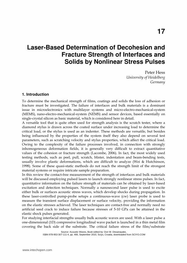
Fig. 1. Setup for tensile interfacial spallation with a pulsed laser, consisting of layers for shock formation, substrate with test film and interferometer to monitor the film surface (Gupta et al., 1990; Wang et al., 2003a).
laser is collimated at the absorbing medium to an area of about 1-3 mm diameter (Gupta et al., 1990). Usually, the elastic pulse is generated by absorption of laser radiation in a ~0.5 µm thick metal (Al) layer, which is sandwiched between the back side of the substrate and an about 10 µm thick transparent confining layer (SiO2, waterglass). Instead of an Al film as
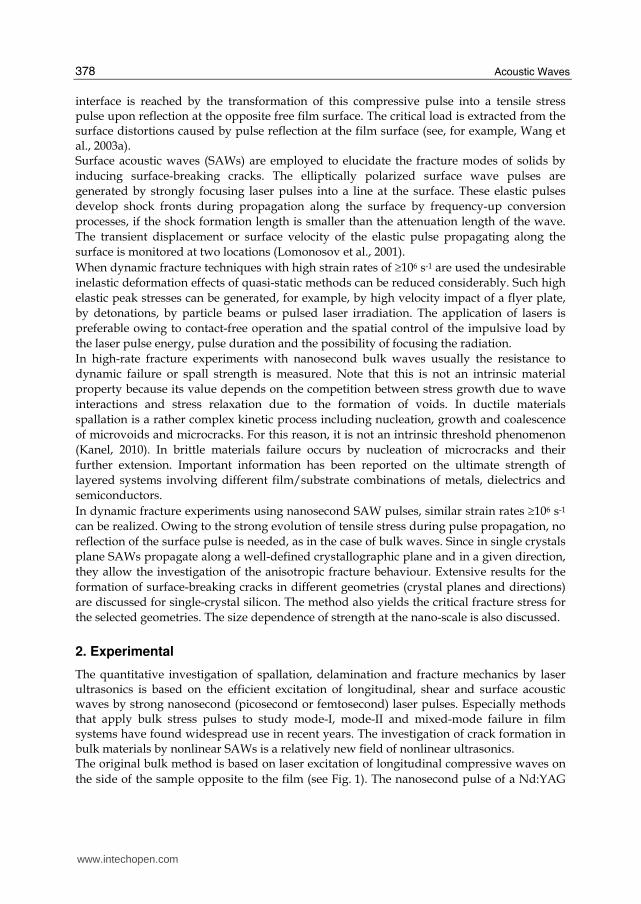
absorbing medium a 20 µm thick layer of silicone grease, containing fine MoS2 particles, has been employed to excite stress waves by laser breakdown (Ikeda et al., 2005). Tensile stress is generated when the compression pulse is reflected from the free film surface. At the surface the resulting stress is zero and reaches its maximum at a distance equal to half of the spatial pulse extension. This restricts the thickness of the films to be delaminated. The situation can be improved by modifying the profile of the stress pulse using an unusual nonlinear property of fused silica, which develops a rarefaction shock at the tail of the pulse for compressive stresses below 4 GPa, as shown in Fig. 1. (Wang et al., 2003a). In this case the tensile stress reaches its maximum at a distance of the width of the post-peak shock, making the method applicable for significantly thinner films. From measurements of the transient out-of-plane displacement or velocity of the free film surface at the epicenter by a laser interferometer, the interfacial strength is obtained for specular and diffuse surfaces using a cw laser as probe (Pronin & Gupta, 1993). Besides longitudinal stress pulses also shear pulses can be obtained by using a triangular fused silica prism for partial mode conversion of the excited longitudinal compressive wave
into a shear wave upon oblique incidence onto a surface, as illustrated in Fig. 2 (Wang et al., 2003b; Wang et al., 2004; Hu & Wang, 2006; Kitey et al., 2009). With an optimized setup, nearly complete conversion into high amplitude shear pulses, and therefore mode-II
fracture by in-plane shear stress, can be achieved at a prism angle of θ = 57.7° (Hu & Wang, 2006). In fact, controlled mixed-mode loading and the quantitative analysis of the stresses involved is possible. It is important to note that in most practical situations thin films tend to fail under mixed-mode I+II conditions. Controlled dynamic delamination of thin films has been achieved recently by insertion of a weak adhesion region below the film to be delaminated (Kandula et al., 2008a). While spallation experiments characterize the interface strength or critical stress for microvoid or microcrack initiation the delamination process can be more closely associated with the propagation of cracks.
www.intechopen.com
Acoustic Waves
380
Modeconversion
Shear Long.
Longitudinal
Confining layer
Absorption layer
ns Laser
Substrate
Film
Interferometer
L1
L2S
1
A B
Fig. 2. Setup for shear stress delamination with a pulsed laser, fused-silica prism for mode conversion and interferometer to monitor the film surface (Hu & Wang, 2006).
In only a few studies have femtosecond lasers been employed to investigate spallation of metal targets (Tamura et al., 2001). With such ultrashort laser pulses ultrafast strain rates of
≥108 s-1 may be accessible. These laser pulses with intensities in the 1015 W/cm2 range launch shock pulses with a steep unloading stress profile. The effects of femtosecond laser-driven shocks using very high laser pulse energies have been described recently based on time-resolved measurement of the surface velocity by Doppler interferometry (Cuq-Lelandais et al., 2009; de Rességuier et al., 2010). SAWs are guided waves that penetrate approximately one wavelength deep into solids.
Thus, the main part of the elastic energy stays within this depth during wave propagation
along the surface. Note that the elliptically polarized surface waves possess in-plane and
out-of-plane displacements, and thus both a longitudinal and shear component. In the
corresponding pump-probe setup a pulsed nanosecond laser is employed to launch a
nanosecond SAW pulse with finite amplitude, which is sufficiently nonlinear to develop
shocks during propagation (Lomonosov et al., 2001). A distinctive property of SAWs is their
intrinsic tensile stress and its further development during nonlinear pulse evolution. A cw
laser is used for detection of the moving surface distortions at two different surface locations
(Kolomenskii et al., 1997).
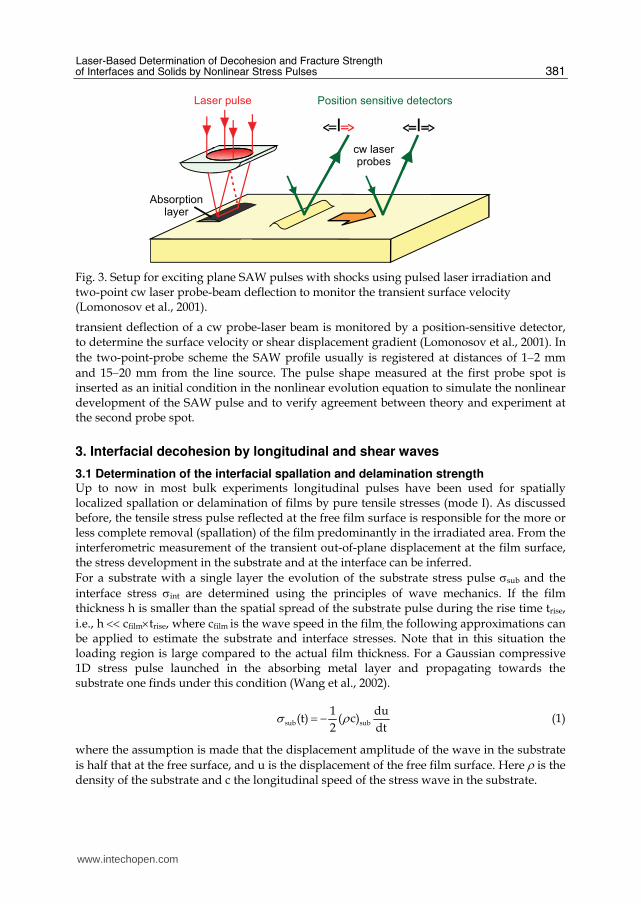
Typically, a Nd:YAG laser radiating at 1.064 µm with 30−160 mJ pulse energy and 8 ns pulse
duration was applied in single-pulse experiments. As depicted in Fig. 3, the explosive
evaporation of a thin layer of a highly absorbing carbon suspension (ink), deposited only in
the source region, is used to launch SAW pulses with sufficient amplitude for nonlinear
evolution. By sharply focusing the pump laser pulse with a cylindrical lens into a narrow
line source, a plane surface wave propagating in a well-defined crystallographic direction is
launched. If the shock formation length is smaller than the attenuation length a propagating
SAW pulse with finite amplitude develops a steep shock front. These nonlinear SAW pulses
gain amplitudes of about 100−200 nm, as compared with few nanometers for linear SAWs.
The shape of the pulse changes not only due to frequency-up conversion but in addition
frequency-down conversion processes take place, caused by the elastic nonlinearity of the
solid. The value of the absolute transient surface displacement can be detected with a
stabilized Michelson interferometer. In most experiments, however, the more versatile
www.intechopen.com
Laser-Based Determination of Decohesion and Fracture Strength of Interfaces and Solids by Nonlinear Stress Pulses
381
Position sensitive detectorsLaser pulse
cw laserprobes
Absorptionlayer
Fig. 3. Setup for exciting plane SAW pulses with shocks using pulsed laser irradiation and two-point cw laser probe-beam deflection to monitor the transient surface velocity (Lomonosov et al., 2001).
transient deflection of a cw probe-laser beam is monitored by a position-sensitive detector, to determine the surface velocity or shear displacement gradient (Lomonosov et al., 2001). In
the two-point-probe scheme the SAW profile usually is registered at distances of 1−2 mm
and 15−20 mm from the line source. The pulse shape measured at the first probe spot is inserted as an initial condition in the nonlinear evolution equation to simulate the nonlinear development of the SAW pulse and to verify agreement between theory and experiment at the second probe spot.
3. Interfacial decohesion by longitudinal and shear waves
3.1 Determination of the interfacial spallation and delamination strength Up to now in most bulk experiments longitudinal pulses have been used for spatially localized spallation or delamination of films by pure tensile stresses (mode I). As discussed before, the tensile stress pulse reflected at the free film surface is responsible for the more or less complete removal (spallation) of the film predominantly in the irradiated area. From the interferometric measurement of the transient out-of-plane displacement at the film surface, the stress development in the substrate and at the interface can be inferred.
For a substrate with a single layer the evolution of the substrate stress pulse σsub and the
interface stress σint are determined using the principles of wave mechanics. If the film thickness h is smaller than the spatial spread of the substrate pulse during the rise time trise,
i.e., h << cfilm×trise, where cfilm is the wave speed in the film, the following approximations can be applied to estimate the substrate and interface stresses. Note that in this situation the loading region is large compared to the actual film thickness. For a Gaussian compressive 1D stress pulse launched in the absorbing metal layer and propagating towards the substrate one finds under this condition (Wang et al., 2002).
sub sub
1 du(t) ( c)
2 dtσ ρ= − (1)
where the assumption is made that the displacement amplitude of the wave in the substrate
is half that at the free surface, and u is the displacement of the free film surface. Here ρ is the density of the substrate and c the longitudinal speed of the stress wave in the substrate.
www.intechopen.com
Acoustic Waves
382
The tensile stress acting at the film/substrate interface can be estimated by assuming that
the stress is given by (ρh)film multiplied by the acceleration of the free surface
2
int film 2
d u(t) ( h)
dtσ ρ= − (2)
The subscripts ‘sub’ and ‘film’ represent substrate and film properties, respectively. When the film thickness becomes comparable to the spatial extension of the rising part of the
pulse, i.e., h ≈ cfilm × riset , the following equation provides a more accurate 1D description of
the stress history at the interface, because in reality the stress loading of the interface results from the superposition of the incoming compressive wave and the reflected tensile pulse
int film film film
1(t,h) ( ) v(t h / c ) v(t h / c )
2cσ ρ= + − −⎡ ⎤⎣ ⎦ (3)
Here v is the measured surface velocity v = du/dt (Gupta et al., 2003). For small values of h/cfilm this equation transforms into Equation (2), which is analogous to Newton’s second law of motion, stating that the interface tensile strength is given by the mass density of the film times the outward acceleration of the centre of mass of the film (Wang et al., 2002). These 1D approximations provide physical insight into the relevant stress loading processes. Numerical simulations are needed to obtain a more accurate description of the three-dimensional evolution of the stress field. The treatment of the more complicated mixed-mode case, where tensile and shear stresses
act simultaneously, can be found in several publications (Wang et al., 2003b); Wang et al.,
2004; Hu & Wang, 2006; Kitey et al., 2009). In these reports the equations have been derived
that are needed to extract the interfacial adhesion strengths for mixed-mode failure and to
compare these results with those for purely tensile loading.
Here the derivation is presented for an experimental arrangement similar to the one shown
in Fig. 2, where the shear wave travels nearly perpendicular to the film surface (φ = 60° and γ
≈ 86.9°), following Hu and Wang (2006). The stress waves S1 and L2 load the film interface
with different mode-mixities at points A and B. At these points another mode conversion
takes place, when S1 and L2 reach the film surface. The out-of-plane displacements u⊥A and
u⊥B and the in-plane displacements u||A and u||B can be calculated as a function of L1, S1,
and L2 (Hu & Wang, 2006). The results indicate that the out-of-plane displacement at point B
is about 2.5 times that at point A.
From the information on the displacements the substrate and interface stresses are derived
on the basis of the 1-D approximation (Hu & Wang, 2006)
22LL
sub sub
du( c )
dtσ ρ= − ` (4)
11SS
sub s sub
du( c )
dtτ ρ= − (5)
2
X Xfilm film 2
d u( h)
dtσ ρ ⊥= − (6)
www.intechopen.com
Laser-Based Determination of Decohesion and Fracture Strength of Interfaces and Solids by Nonlinear Stress Pulses
383
2
X ll Xint film 2
d u( h)
dtτ ρ= − (7)
where the normal and shear stresses in the substrate at the points X (A or B) caused by L2
and S1 are given by 2Lsubσ and 1S
subτ , respectively (see Fig. 2). The corresponding normal and
shear interface stresses are Xintσ and X
intτ and the out-of-plane and in-plane displacements are
u⊥X and u||X, respectively. The relatively large ratio of the shear to the normal interface
stress of ~14 indicates nearly pure shear loading for this particular configuration of the silica
prism.
3.2 Results of interface spallation and delamination experiments Especially spallation experiments have been performed for a large variety of layered material systems. The controlled delamination of a film is more difficult to achieve, but has been reported recently (Kandula et al., 2008a). In the following results obtained for some characteristic systems are selected to illustrate the potential of this laser-based method to study pure and mixed-mode decohesion of thin films in layered systems.
Si/SixNy/Au system
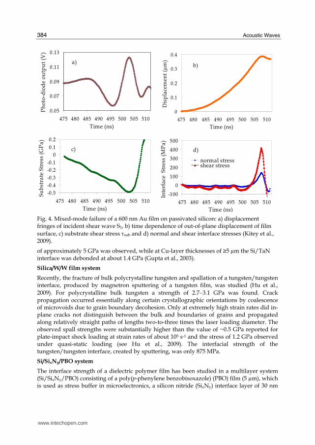
Mixed-mode failure was studied in this particular work using a silicon wafer of 730 nm thickness covered with a SixNy passivation layer (400 nm) and an Au film of thickness of 300 nm, 600 nm, or 1200 nm reported recently (Kandula et al., 2008a). The back side of the silicon substrate was bonded to a fused silica prism equipped with an Al layer (400 nm) and a confining waterglass layer. For the pure tensile strength between the Au film and passivated silicon substrate a critical stress of 245 MPa was found. Under mixed-mode conditions, delamination was observed at about 142 MPa tensile stress and about 436 MPa shear stress. Thus, by applying the shear load the tensile strength was reduced by approximately 100 MPa. The effective stress in the mixed-mode case was about 449 MPa. An interpretation of this finding in comparison with mode-I failure is that mixed-mode decohesion consumes more energy. It is important to note that the laser spallation method clearly yields mode-resolved strength values, whereas the stress fields generated by conventional scratch, peel, pull, blister and indentation tests are difficult to analyze quantitatively due to stress inhomogeneities and plastic deformations involved in these techniques. To illustrate the whole measurement and evaluation procedure of this laser technique, the
registered photo-diode signal is presented in Fig. 4a), the corresponding normal surface
displacement is shown in Fig. 4b), the substrate shear stress is displayed in Fig. 4c) and the tensile and shear stress components acting at the interface are exhibited in Fig. 4d) for a 600 nm Au film deposited on a passivated silicon substrate (Kitey et al., 2009).
Si/TaN/Cu system
In the case of very thin films, the reflected tensile pulse may overlap with the incoming compressive pulse, reducing the effective stress at the interface. In this situation it can happen that the critical fracture strength of the substrate material is first reached at a certain penetration depth of the tensile pulse into the substrate. By increasing the film thickness the incoming and reflected pulse can be separated, finally leading to film spallation. Such a behaviour has been observed for silicon covered by a bilayer of TaN/Cu. The TaN layer thickness was fixed at 20 nm, whereas the Cu layer was varied in five steps between 100 nm and 10 µm. At a Cu-layer thickness ≤1 µm, silicon fracture with an intrinsic tensile strength
www.intechopen.com
Acoustic Waves
384
a)
0.05
0.07
0.09
0.11
0.13
475 480 485 490 495 500 505 510
Time (ns)
Ph
oto
-dio
de
ou
tpu
t (V
)
b)
0
0.1
0.2
0.3
0.4
475 480 485 490 495 500 505 510
Time (ns)
Dis
pla
cem
ent
(µm
)
c)
-0.5
-0.4
-0.3
-0.2
-0.1
0
0.1
0.2
475 480 485 490 495 500 505 510
Time (ns)
Su
bst
rate
Str
ess
(GP
a)
d)
-100
0
100
200
300
400
500
475 480 485 490 495 500 505 510
Time (ns)
Inte
rfa
ce S
tres
s (M
Pa
)normal stressshear stress
Fig. 4. Mixed-mode failure of a 600 nm Au film on passivated silicon: a) displacement fringes of incident shear wave S1, b) time dependence of out-of-plane displacement of film
surface, c) substrate shear stress τsub and d) normal and shear interface stresses (Kitey et al., 2009).
of approximately 5 GPa was observed, while at Cu-layer thicknesses of ≥5 µm the Si/TaN interface was debonded at about 1.4 GPa (Gupta et al., 2003).
Silica/W/W film system
Recently, the fracture of bulk polycrystalline tungsten and spallation of a tungsten/tungsten interface, produced by magnetron sputtering of a tungsten film, was studied (Hu et al.,
2009). For polycrystalline bulk tungsten a strength of 2.7−3.1 GPa was found. Crack propagation occurred essentially along certain crystallographic orientations by coalescence of microvoids due to grain boundary decohesion. Only at extremely high strain rates did in-plane cracks not distinguish between the bulk and boundaries of grains and propagated along relatively straight paths of lengths two-to-three times the laser loading diameter. The observed spall strengths were substantially higher than the value of ~0.5 GPa reported for plate-impact shock loading at strain rates of about 105 s-1 and the stress of 1.2 GPa observed under quasi-static loading (see Hu et al., 2009). The interfacial strength of the tungsten/tungsten interface, created by sputtering, was only 875 MPa.
Si/SixNy/PBO system
The interface strength of a dielectric polymer film has been studied in a multilayer system (Si/SixNy/PBO) consisting of a poly(p-phenylene benzobisoxazole) (PBO) film (5 µm), which is used as stress buffer in microelectronics, a silicon nitride (SixNy) interface layer of 30 nm
www.intechopen.com
Laser-Based Determination of Decohesion and Fracture Strength of Interfaces and Solids by Nonlinear Stress Pulses
385
or 400 nm thickness and a silicon wafer (Kandula et al., 2008b). Stress wave propagation in this multilayer system was analyzed analytically and numerically, by neglecting the influence of the silicon nitride layer in the analysis. At strain rates of about 107 s-1 and laser
fluences of 65 mJ/mm2, compressive stresses of up to 3.5 GPa could be obtained. Such a stress is sufficient to fracture bulk silicon in certain configurations as observed already before (Wang et al., 2002). As expected, the failure of the film interface was observed at much lower laser fluences and varied strongly with the preparation, treatment and thickness of the PBO layers, yielding an upper tensile interface stress of about 0.35 GPa.
Si/neuron cell system
First experimental results and finite element simulations on the extension of the laser-induced bulk stress wave technique to the investigation of biological samples such as cell/substrate adhesion have been reported (Hu et al., 2006). In this pioneering work the noncontact detachment of neuron cells from a silicon substrate was studied. Since the time scale of the experiment is in the nanosecond range cells remain essentially undisturbed before their detachment, which is not the case with other techniques. While adhesion could be characterized only in terms of the critical Nd:YAG laser fluence, it can be expected that the method will be able to quantify the adhesion strength in the near future. The principal detachment mechanism predicted by the simulations performed is strain-driven failure resulting from the cell’s tendency to flatten and elongate along the substrate (Miller et al., 2010).
4. Fracture of anisotropic crystals by surface acoustic wave pulses
4.1 Determination of the bulk fracture strength With SAWs, strong nonlinearities and very high strains in the range of 0.01 can be realized much more easily than with bulk waves (Lomonosov et al., 2001; Lomonosov & Hess, 2002). As mentioned before, SAWs are guided waves that only penetrate approximately one wavelength deep into the solid. This particular property reduces diffraction losses as compared with acoustic bulk waves. In addition, frequency-up conversion concentrates the energy in an even smaller depth from the surface. For certain crystal geometries the displacements of SAWs are confined to the sagittal plane, defined by the in-plane propagation direction x1 and the surface normal x3. Thus, x2 is normal to the sagittal plane. To extract quantitative values of fracture strengths from experiments with laser-induced SAWs, a theoretical description of shock formation in a SAW pulse with finite amplitude during its propagation in a nonlinear elastic medium is required. A suitable nonlinear evolution equation that also takes into account dispersion of SAWs has been developed to describe solitary surface pulses in layered systems (Lomonosov et al., 2002; Eckl et al., 2004; Hess & Lomonosov, 2010). In systems without a length scale, such as single crystals, the dispersion term is not needed because SAWs are not dispersive. Therefore, in silicon, the profiles of the recorded SAW pulses were simulated by solving the following dispersionless nonlinear evolution equation
*n 0 n' n-n' n' n'-n
0 n' ´n n' n
i B nq F(n' / n)B B 2 (n / n')F * (n / n')B Bτ < < >⎡ ⎤∂ = +⎢ ⎥∂ ⎣ ⎦∑ ∑ (8)
where Bn is the n-th harmonic of the signal, τ the stretched coordinate along the direction of wave propagation, q0 the fundamental wave number and F(x) a dimensionless function. This
www.intechopen.com
Acoustic Waves
386
function describes the efficiency of frequency conversion and depends on the ratio of the second-order to third-order elastic constants of the selected geometry. For example, F(1/2) describes the efficiency of second-harmonic generation. Comparison with experiments showed that this equation provides a quantitative description of nonlinear SAW evolution (Lomonosov & Hess, 2002; Lehmann et al., 2003). Experimentally, the SAW pulse is measured at two surface spots by laser-probe-beam deflection, one 1-2 mm from the source and the other at a distance of 15−20 mm (see Fig. 3). The calibration procedure exploits the predictor-corrector method for the iterative solution of the evolution equation, which connects the Fourier components of the transient profiles measured at the first and the second probe spots. Since the distance between the two probe spots was fixed, the observed changes depend only on the initial magnitude of the absolute strain. The aim was to determine the calibration factor ‘a’, with the dimension [1/volt], in the equation u31 = a×U(t), where u31 is the surface velocity or shear displacement gradient and U(t) is the signal measured at the first probe spot. The solution with correct calibration factor should describe the profile registered at the second probe spot and allows one to estimate the absolute surface strain at any other location, e.g., where a surface crack can be
seen. The spectrum of the initial laser-excited transient was limited to about 200 MHz, mainly due to the laser pulse duration of 8 ns. The purpose was to measure the surface slope at a position close to the source, where frequency components in the gigahertz range are still negligible. As can be clearly seen in Fig. 5, the sharp spikes developed at larger propagation distances could no longer be recorded with the experimental setup. Since in a nonlinear medium like a silicon crystal both frequency-up conversion and frequency-down conversion processes take place, a lengthening of the pulse profile occurs simultaneously with shock formation. This effect is proportional to its magnitude, and therefore the pulse length can be used as a sensitive measure of the nonlinear increase of strain. In particular, when the shock fronts become steeper this quantity can be determined quite accurately (Lomonosov & Hess, 2002; Kozhushko & Hess 2007).
60 80 100 120 140 160
-0.2
-0.1
0.0
0.1
0.2
second spot (meas.)
a = 0.11 (1/V) (sim.)
Pro
be
sig
nal
(v
olt
)
Time (ns)
first spot (meas.)
Fig. 5. Typical pulse shapes measured at the first and second probe spots in silicon. Comparison of the latter experimental profile with the predicted shape with spikes explains the calibration procedure of fitting the length of the pulse (Kozhushko & Hess, 2007).
www.intechopen.com
Laser-Based Determination of Decohesion and Fracture Strength of Interfaces and Solids by Nonlinear Stress Pulses
387
4.2 Results for mode-resolved fracture strength of silicon Up to now there is no generally accepted microscopic theory of brittle fracture of materials, because only simulations are possible on the molecular level. Certainly, dynamic fracture consists of two stages, namely nucleation and subsequent propagation of the crack tip. In the experiments considered here, fracture was induced by intrinsic surface nucleation with SAWs propagating along defined geometries. For some special geometries the shocked SAW
pulse introduced not only a single crack but a whole field of about 50−100 µm long cracks by repetitively fracturing the crystal after a certain additional propagation distance along the surface that was sufficient to restore the shocks. Previous fracture experiments indicate that the {111} plane is the weakest cleavage plane in silicon. Failure usually occurred perpendicular to the SAW propagation direction and extended along one of the Si{111} cleavage planes into the bulk. There are three orthogonal pairs of stress components defining three fracture modes, namely tensile or opening σ11, in-plane shear or sliding σ31 and out-of-plane shear or tearing σ21, briefly called fracture modes I, II and III, respectively. By assuming that the {111} plane is the weakest cleavage plane of silicon, geometries were chosen where the intersection line of the {111} cleavage plane with the free surface was normal to the wave vector of the plane SAW pulse. The four basic cleavage planes provide a set of possible orientations. We studied the geometries Si(112)[111], Si(111)[112], Si(223)[334] and Si(221)[114], which are a subset of the general set of geometries (m m n)[n n 2m], where the particle displacements are confined to the sagittal plane, and therefore only the σ11
opening stress component has a non-zero value at the surface (Kozhushko & Hess, 2008). Note that in the coordinate system associated with tilted cleavage planes the initial σ11 stress can be represented by simultaneously acting orthogonal components, which are associated with a tensile mode and an in-plane shearing mode. The orientation of the family of {111}
cleavage planes, which are normal to the sagittal plane, is displayed in Fig. 6. In all these cases, the initial σ11 opening stress can be represented by two orthogonal components with their ratio defined by the tilt angle of the cleavage plane with respect to the surface normal.
Fig. 6. Crystallographic configurations of the Si{111} cleavage planes normal to the sagittal section, e.g., for the subset of the (m m n)[n n 2m] geometries (Kozhushko & Hess, 2007).
www.intechopen.com
Acoustic Waves
388
In the following discussion results are presented for the low-index planes Si(112), Si(111), Si(223), Si(221) and Si(110) and SAW propagation in selected directions, described in more detail previously (Lomonosov & Hess, 2002; Kozhushko et al., 2007; Kozhushko & Hess, 2007; Kozhushko & Hess, 2008; Kozhushko & Hess, 2010)
Silicon (112) plane
Initiation of impulsive fracture by nonlinear SAW pulses in the Si(112)< 111 > geometry
revealed that SAW pulses propagating in the < 111 > direction induced fracture at
significantly lower laser pulse energies, and thus at lower SAW strains, than the mirror-
symmetric wave propagating in the opposite <11 1 > direction. This surprising effect is a
consequence of differences in the elastic nonlinearity of the two propagation directions.
The easy-cracking configuration was used for fracture experiments with low laser pulse
energies of 30−40 mJ. An optical microscope image of the induced crack field of a typical fractured surface is presented in Fig. 7. The vertical line at the right-hand side is the imprint of the laser-generated line source. The position of the first probe spot was approximately 0.5 mm from the source. With further propagation the finite SAW pulse developed the critical stress needed for fracture. At a distance of about 1 mm from the source the first crack can be seen. For crack nucleation and formation of the crack faces a certain amount of energy is needed. The resulting loss in pulse energy mainly reduces the high frequency part of the SAW pulse spectrum. The crack field extending further to the left-hand side is the result of repetitive fracture processes, occurring due to repetitive recovery of the shock fronts during propagation after each fracture event.
On the surface the cracks extended into the < 110 > direction, perpendicular to the SAW
propagation direction and sagittal plane, with a length of up to 50 µm, controlled by the
length of the SAW pulse in the nanosecond range. As expected, failure occurred along the
intersection line of the surface with the {11 1 } cleavage plane (see Fig. 6). The resulting peak
value of the σ11 stress at the surface is associated with the tensile strength of the material for
nucleation of cracks at the surface. A series of experiments yielded about 4.5 GPa for the
critical opening stress of silicon at the surface in this particular geometry. Note that here
only normal stress acts on the {11 1 } cleavage plane, which is perpendicular to the surface
for this particular geometry, and consequently the nucleation of cracks can be considered as
a pure mode-I process (Kozhushko & Hess, 2007).
Fig. 7. Optical microscope image of the Si(112) surface after propagation of a single
nonlinear SAW pulse in the < 111 > direction from the source on the right side to the left
(Kozhushko & Hess, 2007).
www.intechopen.com
Laser-Based Determination of Decohesion and Fracture Strength of Interfaces and Solids by Nonlinear Stress Pulses
389
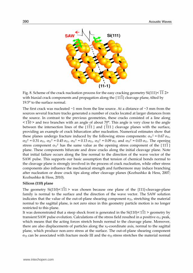
Silicon (111) plane
For this geometry we also made the observation that counterpropagating nonlinear SAW
pulses, moving in opposite directions, e.g., in the < 11 2> and <11 2 > directions on the
Si(111) plane, develop completely different nonlinear pulse shapes. In the easy-cracking
geometry Si(111) < 112 > the tensile fracture strength was in the range of about 4 GPa. The
surface-nucleated cracks propagated into the bulk along the {11 1 } cleavage plane, which is
inclined by 19.5° to the normal of the free surface (see Fig. 6). According to the boundary
conditions for SAWs, only the tensile opening stress σ11 is nonzero at the surface in the
initial coordinate system.
This tensile stress of σ11 = 4 GPa can be represented by a set of orthogonal components in the
coordinate system associated with the tilted cleavage plane { 111} . The stresses in the new
coordinate system are calculated by applying the transformation rule σij = AikAjlσkl, where
Aik is the corresponding rotation matrix around x2. As in the initial coordinate system only
σ11 has a non-zero value at the surface, we find the tensile stresses σ11T(t) = cos2ϕσ11(t) and
σ33T (t) = sin2ϕσ11(t), and the shearing stress components σ13T(t) = σ31T = −(1/2)sin2ϕσ11(t),
where x1T is normal to the { 111 } cleavage plane and ϕ is the angle of rotation around x2. In
the following estimate the time dependence will be omitted. The amplitudes of the
calculated stress components were reduced according to the transformation law. The mean
value of the predicted σ11 stress at the first fracture point is 4.0 GPa. The value of σ11T is
equal to 3.6 GPa and can be considered as an estimate of the fracture strength of silicon in
this special geometry (Kozhushko et al., 2007; Lomonosov & Hess, 2008).
In fact, a combination of mode I (tensile opening) and mode II (in-plane shearing or sliding)
processes is expected to control this fracture geometry. The resulting stress components for
a biaxial fracture mechanism in the tilted coordinate system are σ11T = 3.6 GPa and σ31T = –1.3
GPa. In addition, a smaller contribution from the component σ33T = 0.4 GPa has to be taken
into account in a rigorous treatment. Fig. 8 illustrates the ‘biaxial’ fracture components with
respect to the {11 1 } cleavage plane for this geometry (Kozhushko & Hess, 2010).
Silicon (223) plane
A very small tilt of the cleavage plane from the surface normal of 8° (see Fig. 6) generates a
σ31T component acting as sliding mode of fracture along the {11 1 } cleavage plane with a
value of σ31T = −0.14 σ11. Since fracture is a dynamic process, even such a relatively small
shear stress may play an important role during crack extension. The other components are
σ11T = 0.98 σ11 and σ33T = 0.02 σ11. A series of such experiments resulted in a critical fracture
strength of only σ11 ≈ 3.0 GPa in this geometry, the lowest critical opening stress found for
the investigated geometries (Kozhushko & Hess, 2010).
Silicon (221) plane
In this fracture geometry the tilt of the cleavage plane is 35.3° to the surface normal (see Fig.
6). A laser pulse energy of about 70 mJ had to be applied to achieve fracture in the easy
cracking direction, namely the Si(221)< 11 4> geometry. As the stress acting normal to the
{ 111} cleavage plane is reduced to 2/3 of the initial σ11 stress at the surface, all components
can be easily obtained as described above as σ11T = 0.67 σ11, σ31T = −0.48 σ11 and σ33T = 0.33 σ11.
It is noteworthy that nearly half of the initial tensile stress of σ11 = 3.5 GPa is transformed to
an in-plane-shearing action in this case.
www.intechopen.com
Acoustic Waves
390
{11-1}
Si(111)SAW
Fig. 8. Scheme of the crack nucleation process for the easy cracking geometry Si(111)< 11 2>
with biaxial crack components and propagation along the { 111} cleavage plane, tilted by
19.5° to the surface normal.
The first crack was nucleated ~1 mm from the line source. At a distance of ~3 mm from the
sources several fracture tracks generated a number of cracks located at larger distances from
the source. In contrast to the previous geometries, these cracks consisted of a line along
< 110 > and two branches with an angle of about 70°. This angle is very close to the angle
between the intersection lines of the { 111 } and { 111 } cleavage planes with the surface,
providing an example of crack bifurcation after nucleation. Numerical estimates show that
these planes undergo fracture induced by the following stress components: σ11T = 0.67 σ11,
stress component σ11T has the same value as the opening stress component of the { 111 }
plane. These components bifurcate and draw cracks along the initial cleavage plane. Note
that initial failure occurs along the line normal to the direction of the wave vector of the
SAW pulse. This supports our basic assumption that tension of chemical bonds normal to
the cleavage plane is strongly involved in the process of crack nucleation, while other stress
components also influence the mechanical strength and furthermore may induce branching
after nucleation or draw crack tips along other cleavage planes (Kozhushko & Hess, 2007;
Kozhushko & Hess, 2010).
Silicon (110) plane
The geometry Si(110)< 111 > was chosen because one plane of the {111}-cleavage-plane
family is normal to the surface and the direction of the wave vector. The SAW solution
indicates that the value of the out-of-plane shearing component σ21, stretching the material
normal to the sagittal plane, is not zero since in this geometry particle motion is no longer
restricted to this plane.
It was demonstrated that a steep shock front is generated in the Si(110)< 111 > geometry by
transient SAW pulse evolution. Calculations of the stress field resulted in a positive σ11 peak,
which means that the acting forces stretch bonds normal to the cleavage plane. Moreover,
there are also displacements of particles along the x2-coordinate axis, normal to the sagittal
plane, which produce non-zero stress at the surface. The out-of-plane shearing component
σ21 can be associated with fracture mode III and the σ22 stress stretches the material normal
www.intechopen.com
Laser-Based Determination of Decohesion and Fracture Strength of Interfaces and Solids by Nonlinear Stress Pulses
391
to the sagittal plane. These contributions, however, are relatively small, since the analysis
yields σ11/σ21 ≈ 15 and σ11/σ22 ≈ 7 for the peak stress components at the surface.
Dynamic fracture under the predominant action of biaxial stresses in the Si(110)< 111 >
geometry was studied to further examine a more complicated mixed case. There is no
difference for nonlinear pulse evolution of counterpropagating SAWs in this particular
geometry. Fracture could be achieved only by increasing the laser pulse energy up to about
150 mJ and no extensive crack field could be observed. The average value found for the
initial critical tensile stress σ11 was about 7 GPa. The transformation of the coordinate system
of the SAW solution to the fracture geometry gives the following estimates of the peak stress
components for the second plane normal to the free surface, namely { 111 }, in comparison
with the initial { 111 } cleavage plane: σ11T = 0.2 σ11, σ21T = 0.22 σ11 and σ22T = 0.95 σ11. These
components are strong enough to branch the nucleated crack (Kozhushko & Hess, 2007;
Kozhushko & Hess, 2010).
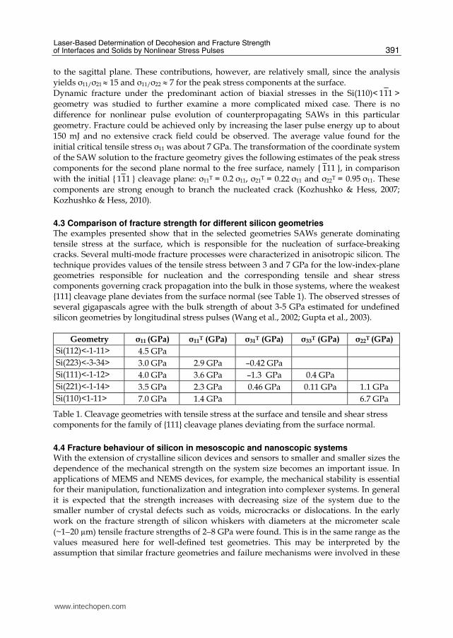
4.3 Comparison of fracture strength for different silicon geometries The examples presented show that in the selected geometries SAWs generate dominating tensile stress at the surface, which is responsible for the nucleation of surface-breaking cracks. Several multi-mode fracture processes were characterized in anisotropic silicon. The technique provides values of the tensile stress between 3 and 7 GPa for the low-index-plane geometries responsible for nucleation and the corresponding tensile and shear stress components governing crack propagation into the bulk in those systems, where the weakest {111} cleavage plane deviates from the surface normal (see Table 1). The observed stresses of several gigapascals agree with the bulk strength of about 3-5 GPa estimated for undefined silicon geometries by longitudinal stress pulses (Wang et al., 2002; Gupta et al., 2003).
Table 1. Cleavage geometries with tensile stress at the surface and tensile and shear stress components for the family of {111} cleavage planes deviating from the surface normal.
4.4 Fracture behaviour of silicon in mesoscopic and nanoscopic systems With the extension of crystalline silicon devices and sensors to smaller and smaller sizes the dependence of the mechanical strength on the system size becomes an important issue. In applications of MEMS and NEMS devices, for example, the mechanical stability is essential for their manipulation, functionalization and integration into complexer systems. In general it is expected that the strength increases with decreasing size of the system due to the smaller number of crystal defects such as voids, microcracks or dislocations. In the early work on the fracture strength of silicon whiskers with diameters at the micrometer scale
(~1−20 µm) tensile fracture strengths of 2−8 GPa were found. This is in the same range as the values measured here for well-defined test geometries. This may be interpreted by the assumption that similar fracture geometries and failure mechanisms were involved in these
www.intechopen.com
Acoustic Waves
392
processes. In more recent experiments using nanowires with diameters of 700 to 100 nm the
strength increased from 0.03 to 2−4 GPa (Gordon et al., 2009). For the mechanical properties of self-welded [111] single-crystal silicon nanowire bridges, grown between two silicon posts, the maximum bending stress increased from 300 to 830 MPa for a wire diameter decreasing from 200 to 140 nm, depending on the loading conditions (Tabib-Azar et al., 2005). This means that at the micrometer scale the mechanical strength of the best silicon materials is comparable with the strength of wafers at the millimeter scale. This is consistent with the observation that size effects do not play a role on the elastic behaviour of silicon nanowires with a diameter >100 nm (Sohn et al., 2010). In recent years, several techniques such as the chemical vapor deposition (CVD) vapor liquid solid (VLS) or CVD-VLS method have been developed to grow nanowires with diameters down to the few nanometer range. Currently, however, it is very difficult to extract general conclusions from this pioneering work, since contradictory results have been reported for the size effects of mechanical properties. It seems that the strength of silicon can
increase to about 12 GPa, as the nanowire diameter decreases to 100−200 nm (Hoffmann et
al., 2006) and 15−60 nm (Zhu et al., 2009) in wires grown along the [111] direction. This value comes already near to the theoretical strength for tensile cleavage of silicon along the
{111} plane of 22 GPa obtained by ab initio calculations for an ideal silicon lattice (Roundy & Cohen, 2010). A similar value of 21 GPa has been reported by Dubois et al. in 2006. In Fig. 9 the strength values measured for macroscopic, mesoscopic and nanoscopic silicon systems are compared with ab initio theory of an ideal silicon crystal. It is interesting to note that for silicon the difference between the highest measured and ideal strength is only a factor of two, while it is 1-2 orders of magnitude for diamond (Hess, 2009). Nanowires with a diameter below 20 nm can grow in the [111], [110] and [112] directions. For [110]-oriented nanowires with diameter <60 nm ductile failure has been observed (Han
et al., 2007), while for [111]-oriented wires with diameters of 100−200 nm brittle failure occurred without plastic deformation (Heidelberg et al., 2006). These findings point to changes in the fracture behaviour at the nano-scale, which seem to be connected with the increasing surface/volume ratio and a smaller influence of defects.
25
20
15
10
5
macro-scale
meso-scale
nano-scale
ab initiocalculation
Fra
ctu
re s
trength
(G
Pa)
Si wafermillimeter
Si whiskermicrometer
Si nano-wirenanometer
Siliconideal crystal
Fig. 9. Comparison of theoretical and experimental strength values for ideal and real silicon systems with decreasing size.
www.intechopen.com
Laser-Based Determination of Decohesion and Fracture Strength of Interfaces and Solids by Nonlinear Stress Pulses
393
4.5 Molecular dynamics simulation of molecular silicon fracture mechanisms Ab initio calculations are quite accurate but up to now provided only the brittle fracture strength of a few selected low-index failure configurations of silicon without detailed mechanistic information on the dynamics of the rearrangement of bonds. It is important to note that brittle fracture is a complicated multi-scale phenomenon involving nanoscopic and mesoscopic length scales. Atomic-scale crack growth proceeds via individual bond breaking events of variously oriented bonds depending on crack speed, which controls the individual propagation steps of fracture. These fundamental processes can be studied by simulations combining classical potentials and quantum mechanics, describing the stress fields and chemical rearrangements at the crack tip. For silicon such simulations have been performed giving new insight into the various possibilities of crack nucleation and extension. In the well studied case of cracking along the Si{111} cleavage plane, for example, it is possible to discriminate between clean continuous propagation of a crack along {111} by breaking six-member rings and discontinuous fracture by the formation of five- and seven-member rings in a recontruction process, as illustrated in Fig. 10. In the bulk, plastic deformation along the dislocation glide is prohibited if the Peierls stress for the movement of nucleated dislocations is too high, as assumed for low temperatures (Kermode et al., 2008). Recent simulations of the fracture mechanism in silicon nanowires by the modified
embedded atom method (MEAM) potential indicate that cleavage is initiated by nucleation
of a surface microcrack, while shear failure is initiated by the nucleation of a dislocation at
the surface (Kang & Cai, 2010). Contrary to the situation in the bulk, failure seems to be
controlled by the nucleation of dislocations and not by the dislocation mobility in these nano
Fig. 10. Illustration of two different cracking modes of silicon: a) clean continuous crack propagation along {111} by breaking six-member rings and b) discontinuous fracture by the formation of five- and seven-member rings. The dashed line indicates the dislocation glide.
systems. It is interesting to note that nanowires with a diameter below 4 nm fail by shear processes at any temperature. For nanowires with a diameter >4 nm these simulations
predict a fracture stress of 13 GPa for nanowires grown along the [110] direction and 15 GPa
for the [111] direction, at a strain rate of 5×10⁸ s-1. This indicates that for nanowires with a diameter in the nanometer range the fracture strength of [110] nanowires may be lower than that of the [111] nanowires, contrary to the behaviour of bulk silicon. One has to bear in
www.intechopen.com
Acoustic Waves
394
mind, however that the theoretical strain rates are many orders of magnitude higher than those of conventional fracture techniques, whereas for laser-induced fracture the difference in the strain rate is approximately two orders of magnitude. In fact, the higher strain rates used in the simulations could be the reason for the higher strength, as compared with the experimental value of about 12 GPa. While it is still difficult to compare molecular-dynamics simulations with experiments performed at the same time scale fracture of nanowires allows a comparison with theory at least on the same length scale.
5. Conclusions
Laser-induced stress pulses provide a novel efficient tool to elucidate the mode-specific spallation and delamination of films. Here the shock-pulse method measures the interface strength. In anisotropic crystals intrinsic nucleation at the surface by uni-axial and multi-axial fracture can be studied. The defined loading geometries realized with bulk and surface waves allow a straightforward interpretation in comparison with conventional methods. Therefore, the laser methods provide important insight into the relevant pure mode but also multi-mode failure processes. In fact, the critical stress or failure strength of spallation, delamination, fracture and cleavage can be determined in layered and anisotropic materials. For high-quality materials such as single-crystal silicon the measured critical stress components may be compared with ab initio calculations, performed for well-defined low-index geometries, to judge the mechanical quality of real materials. Owing to the high strain rates (~106 s-1) involved, the influence of plastic deformations is reduced. This usually allows a more sensitive and accurate analysis of the mechanical strength, which is of increasing interest in thin-film technology and sensor device fabrication. The mechanical strength of nano-scale systems such as nanowires is currently under intense investigation. First interesting results on the mechanical response of MEMS structures have been reported (Kimberley et al., 2008). Important mechanistic insight into the atomic-scale processes during crack nucleation and propagation is provided by molecular dynamics simulations.
6. References
Cuq-Lelandais, J.-P.; Boustie, M.; Berthe, L.; de Rességuier, T.; Combis, P.; Colombier, J. P.; Nivard, M. & Claverie, A. (2009). Spallation generated by femtosecond laser driven
shocks in thin metallic targets: J. Phys. D: Appl. Phys., 42, pp. 065402-1−10 Dubois, S. M.-M.; Rignanese, G.-M.; Pardoen, T. & Charlier, J.-C. (2006). Ideal strength of
silicon: An ab initio study: Phys. Rev. B, 74, pp. 235203-1−7 Eckl, C.; Kovalev, A. S.; Mayer, A. P.; Lomonosov, A. M. & Hess, P. (2004). Solitary surface
acoustic waves: Phys. Rev. E, 70, pp. 046604-1−15 Gordon, M. J.; Baron, T.; Dhalluin, F.; Gentile, P. & Ferret, P. (2009). Size effects in mechanical
deformation and fracture of cantilevered silicon nanowires: Nano Lett., 9, pp. 525−529 Gupta, V.; Argon, A. S.; Cornie, J. A. & Parks, D. M. (1990). Measurement of interface
strength by laser-pulse-induced spallation: Mater. Sci. Eng. A, 126, pp. 105−117 Gupta, V.; Kireev, V.; Tian, J.; Yoshida, H. & Akahoshi, H. (2003). Glass-modified stress
waves for adhesion measurement of ultrathin films for device applications: J. Mech.
Phys. Solids, 51, pp. 1395−1412 Han, X.; Zheng, K.; Zhang, Y.; Zhang, X.; Zhang, Z. & Wang, Z. L. (2007). Low- temperature in
situ large-strain plasticity of silicon nanowires: Adv. Mater., 19, 2112−2118
www.intechopen.com
Laser-Based Determination of Decohesion and Fracture Strength of Interfaces and Solids by Nonlinear Stress Pulses
395
Heidelberg, A.; Ngo, L. T.; Wu, B.; Phillips, M. A.; Sharma, S.; Kamins, T. I.; Sader, J. E. & Boland, J. J. (2006). A generalized description of the elastic properties of nanowires: Nano Lett., 6, pp. 1101−1106
Hess, P. (2009). Determinetion of linear and nonlinear mechanical properties of diamond by laser-based acoustic waves: Diamond Relat. Mater., 18, pp. 186-190
Hess, P. & Lomonosov, A. M. (2010). Solitary surface acoustic waves and bulk solitons in nanosecond and picosecond laser ultrasonics: Ultrasonics, 50, pp. 167−171
Hoffmann, S.; Utke, I.; Moser, B.; Michler, J.; Christiansen, S. H.; Schmidt, V.; Senz, S.; Werner, P.; Gösele, U. & Ballif, C. (2006). Measurement of the bending strength of vapor-liquid-solid grown silicon nanowires: Nano Lett., 6, pp. 622−625
Hu, L. & Wang, J. (2006). Pure-shear failure of thin films by laser-induced shear waves: Exp. Mech., 46, pp. 637−645
Hu, L.; Zhang, X.; Miller, P.; Ozkan, M.; Ozkan, C. & Wang, J. (2006). Cell adhesion measurement by laser-induced stress waves: J. Appl. Phys., 100, pp. 084701-1−5
Hu, L.; Miller, P. & Wang, J. (2009). High strain-rate spallation and fracture of tungsten by laser-induced stress waves: Mater. Sci. Eng. A, 504, pp. 73−80
Ikeda, R.; Cho, H.; Sawabe, A. & Takemoto, M. (2005). Laser spallation method to measure strength against mode-I decohesion of CVD diamond films: Diamond Relat. Mater., 14, pp. 631−636
Kandula, S. S. V.; Tran, P.; Geubelle, P. H. & Sottos, N. R. (2008a). Dynamic delamination of patterned thin films: Appl. Phys. Lett., 93, pp. 261902-1−3
Kandula, S. S. V.; Hartfield, C. D.; Geubelle, P. H. & Sottos, N. R. (2008b). Adhesion strength measurement of polymer dielectric interfaces using laser spallation technique: Thin Solid Films, 516, pp. 7627−7635
Kanel, G. I. (2010). Spall fracture methodological aspects, mechanisms and governing factors: Int. J. Fract. DOI: 10.1007/s10704-009-9438-0
Kang, K. & Cai, W. (2010). Size and temperature effects on the fracture mechanisms of silicon nanowires: Molecular dynamics simulations: Int. J. Plasticity, DOI: 10.1016/j.ijplas. 2010 .02.001
Kermode, J. R.; Albaret, T.; Sherman, D.; Bernstein, N.; Gumbsch, P.; Payne, M. C.; Csányi, G. & De Vita, A. (2008). Low-speed fracture instabilities in a brittle crystal: Nature, 455, pp. 1224−1227
Kimberley, J.; Chasiotis, I. & Lambros, J. (2008). Failure of microelectromechanical systems subjected to impulsive load: Int. J. of Solids and Struct., 45, pp. 497−512
Kitey, R.; Geubelle, P. H. & Sottos, N. R. (2009). Mixed-mode interfacial adhesive strength of a thin film on an anisotropic substrate: J. Mech. Phys. Solids, 57, pp. 51−66
Kolomenskii, A. A.; Lomonosov, A. M.; Kuschnereit, R.; Hess, P. & Gusev, V. E. (1997). Laser generation and detection of strongly nonlinear elastic surface pulses: Phys. Rev. Lett., 79, pp. 1325−1328
Kozhushko, V. V. & Hess, P. (2007). Anisotropy of the strength of Si studied by a laser-based contact-free method: Phys. Rev. B, 76, pp. 144105-1−11
Kozhushko, V. V. & Hess, P. (2008). Nonlinear surface acoustic waves: silicon strength in phonon-focusing directions: Ultrasonics, 48, pp. 488−491
Kozhushko, V. V. & Hess, P. (2010). Comparison of mode-resolved fracture strength of silicon with mixed-mode failure of diamond crystals: Eng. Fract. Mech., 77, pp. 193−200
Kozhushko, V. V.; Lomonosov, A. M. & Hess, P. (2007). Intrinsic strength of silicon crystals in pure- and combined-mode fracture without precrack, Phys. Rev. Lett., 98, pp. 195505-1−4
www.intechopen.com
Acoustic Waves
396
Lacombe, R. H. (2006). Adhesion Measurement Methods: Theory and Practice, CRC Press, ISBN 0-8247-5361-5, Boca Raton, FL
Lehmann, G.; Lomonosov, A. M.; Hess, P. & Gumbsch, P. (2003). Impulsive fracture of fused quartz and silicon crystals by nonlinear surface acoustic waves: J. Appl. Phys., 94,
pp. 2907−2914 Lomonosov, A. M. & Hess, P. (2002). Impulsive fracture of silicon by elastic surface pulses
with shocks: Phys. Rev. Lett., 89, pp. 095501-1−4 Lomonosov, A. M., Hess, P. & Mayer, A. P. (2002). Observation of solitary elastic surface
pulses: Phys. Rev. Lett., 88, pp. 076104-1−4 Lomonosov, A. M.; Mayer, A. P. & Hess, P. (2001). Laser-based surface acoustic waves in
materials science, In: Modern Acoustical Techniques for the Measurement of Mechanical Properties, Levy, M.; Bass, H. E. & Stern R. (Eds.), pp. 65-134, Academic, ISBN 0-12-475786-6, San Diego, CA
Lomonosov, A. M. & Hess, P. (2008). Nonlinear surface acoustic waves: Realization of solitary pulses and fracture: Ultrasonics, 48, pp. 482-487
Miller, P.; Hu, L. & Wang, J. (2010). Finite element simulation of cell-substrate decohesion by laser-induced stress waves: Mech. Behav. Biomed. Mater., 3, pp. 268−277
Pronin, A. & Gupta, V. (1993). Interferometry on diffuse surfaces in high-velocity
measurements: Rev. Sci. Instrum., 64, pp. 2233−2236 De Rességuier, T.; Cuq-Lelandais, J.-P.; Boustie, M.; Lescoute, E. & Berthe, L. (2010). Wave
propagation and dynamic fracture in laser shock-loaded solid materials, In: Wave Propagation in Materials for Modern Applications, Petrin, A. (Ed.), pp. 419-436, INTECH, ISBN 978-953-7619-65-7, Croatia
Roundy, D. & Cohen, M. L. (2001). Ideal strength of diamond, Si, and Ge: Phys. Rev. B, 64,
pp. 212103-1−3 Sohn, Y.-S.; Park, J.; Yoon, G.; Song, J.; Jee S.-W.; Lee, J.-H.; Na, S.; Kwon, T. & Eom, K.
(2010). Mechanical properties of silicon nanowires: Nanoscale Res. Lett., 5, pp. 211-216 Tabib-Azar, M.; Nassirou, M.; Wang, R.; Sharma, S.; Kamins, T. I.; Islam, M. S. & Williams,
R. S. (2005). Mechanical properties of self-welded silicon nanobridges: Appl. Phys.
Lett., 87, pp. 113102-1−3 Tamura, H.; Kohama, T.; Kondo, K. & Yoshida M. (2001). Femtosecond-laser-induced
spallation in aluminum: J. Appl. Phys., 89, pp. 3520−3522 Wang, J.; Weaver, R. L. & Sottos, N. R. (2002). A parametric study of laser induced thin film
spallation: Exp. Mech., 42, pp. 74−83 Wang, J.; Weaver, R. L. & Sottos, N. R. (2003a). Laser-induced decompression shock
development in fused silica: J. Appl. Phys., 93, pp. 9529−9536 Wang, J.; Sottos, N. R. & Weaver, R. L. (2003b). Mixed-mode failure of thin films using laser-
generated shear waves: Exp. Mech., 43, pp. 323−330 Wang, J.; Sottos, N. R. & Weaver, R. L. (2004). Tensile and mixed-mode strength of a thin
film-substrate interface under laser-induced pulse loading: J. Mech. Phys. Solids, 52,
pp. 999−1022 Wei, Y. & Hutchinson, J. W. (1998). Interface strength, work of adhesion and plasticity in the
peel test: Int. J. Fract., 93, pp. 315−333 Zhu, Y.; Xu, F.; Qin, Q.; Fung, W. Y. & Lu, W. (2009). Mechanical properties of vapor-
liquid−solid synthesized silicon nanowires: Nano Lett., 9, pp. 3934−3939
www.intechopen.com
Acoustic WavesEdited by Don Dissanayake
ISBN 978-953-307-111-4Hard cover, 434 pagesPublisher SciyoPublished online 28, September, 2010Published in print edition September, 2010
InTech ChinaUnit 405, Office Block, Hotel Equatorial Shanghai No.65, Yan An Road (West), Shanghai, 200040, China
Phone: +86-21-62489820
SAW devices are widely used in multitude of device concepts mainly in MEMS and communication electronics.As such, SAW based micro sensors, actuators and communication electronic devices are well knownapplications of SAW technology. For example, SAW based passive micro sensors are capable of measuringphysical properties such as temperature, pressure, variation in chemical properties, and SAW basedcommunication devices perform a range of signal processing functions, such as delay lines, filters, resonators,pulse compressors, and convolvers. In recent decades, SAW based low-powered actuators and microfluidicdevices have significantly added a new dimension to SAW technology. This book consists of 20 excitingchapters composed by researchers and engineers active in the field of SAW technology, biomedical and otherrelated engineering disciplines. The topics range from basic SAW theory, materials and phenomena toadvanced applications such as sensors actuators, and communication systems. As such, in addition totheoretical analysis and numerical modelling such as Finite Element Modelling (FEM) and Finite DifferenceMethods (FDM) of SAW devices, SAW based actuators and micro motors, and SAW based micro sensors aresome of the exciting applications presented in this book. This collection of up-to-date information and researchoutcomes on SAW technology will be of great interest, not only to all those working in SAW based technology,but also to many more who stand to benefit from an insight into the rich opportunities that this technology hasto offer, especially to develop advanced, low-powered biomedical implants and passive communicationdevices.
How to referenceIn order to correctly reference this scholarly work, feel free to copy and paste the following:
Peter Hess (2010). Laser-based Determination of Decohesion and Fracture Strength of Interfaces and Solidsby Nonlinear Stress Pulses, Acoustic Waves, Don Dissanayake (Ed.), ISBN: 978-953-307-111-4, InTech,Available from: http://www.intechopen.com/books/acoustic-waves/laser-based-determination-of-decohesion-and-fracture-strength-of-interfaces-and-solids-by-nonlinear-