Laser Induced Periodic Surface Structures: from physical phenomena to industrial applications Prof. Leonardo Orazi Department of Sciences and Methods for Engineering Manufacturing and Technology Group Department of Sciences and Methods for Engineering Campus San Lazzaro - Reggio Emilia
Transcript
Laser Induced Periodic Surface Structures: from physical phenomena to industrial
applications
Prof. Leonardo Orazi
Department of Sciences and Methods for Engineering Manufacturing and Technology Group
Department of Sciences and Methods for Engineering Campus San Lazzaro - Reggio Emilia
Manufacturing and Technology Group @ DISMI
2Department of Sciences and Methods for Engineering Manufacturing and Technology Group
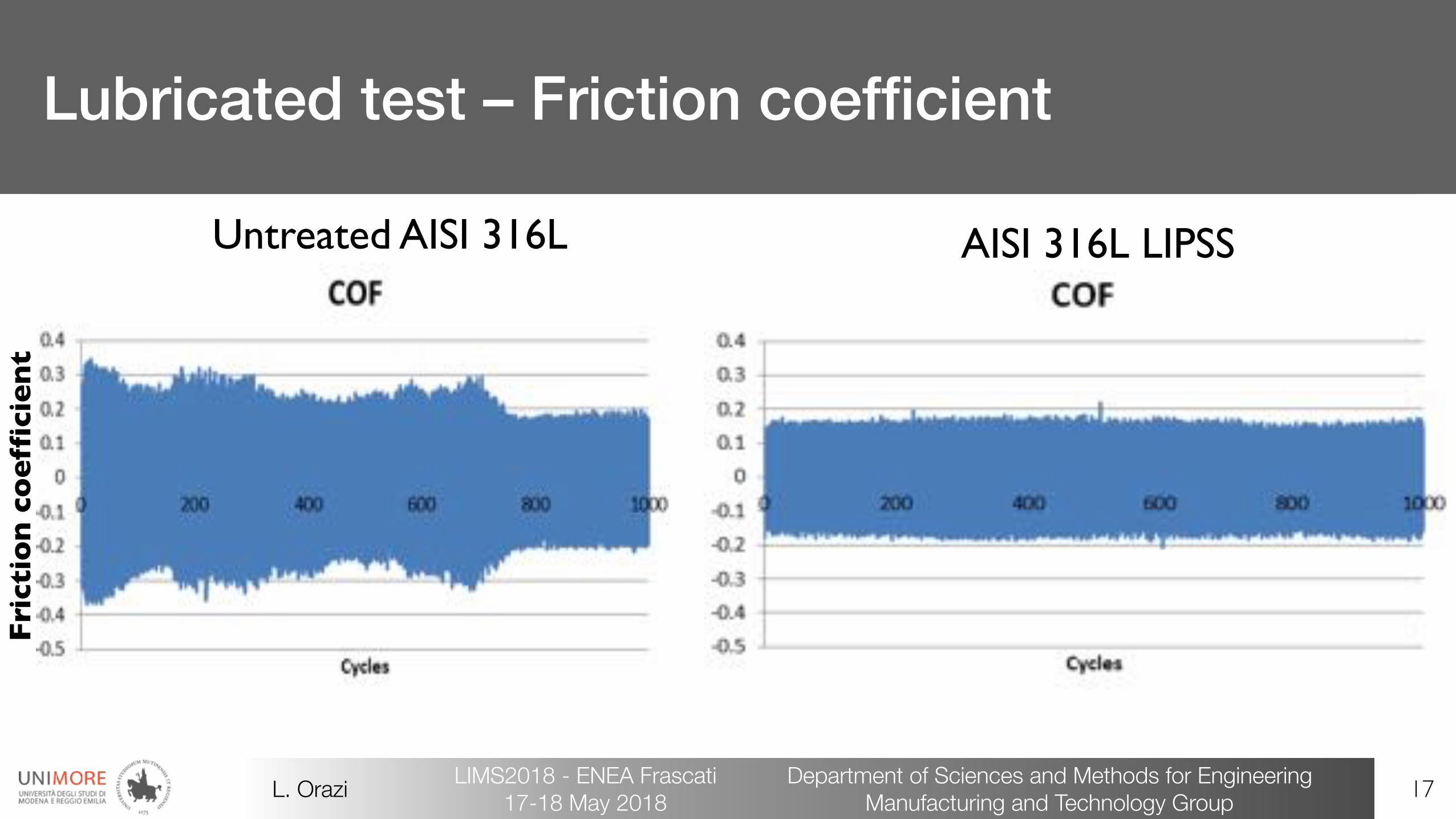
LIMS2018 - ENEA Frascati 17-18 May 2018L. Orazi
Department of Sciences and Methods for Engineering
• Management and Production Engineering
• Mechatronics
Laser texturing as a tool to improve surface characteristics
4Department of Sciences and Methods for Engineering Manufacturing and Technology Group
LIMS2018 - ENEA Frascati 17-18 May 2018L. Orazi
Tecnologie Speciali Lavorazioni Laser
Θ0
"2x0 "x0 x0 2x0x
"2R0
"R0
R0
2R0
R!x"
Figura 5.27: Geometria del fascio gaussiano
!2x0 !x0 x0 2x0x
0.250.50.75
1
I!0,Ρ"#I0
Figura 5.28: Intensita sull’asse del fascio gaussiano
La potenza totale viene calcolata con la solita
P =
! ∞
0
! 2π
0I (x, ρ, θ) ρ dθ dρ = 2π
! ∞
0I (x, ρ) ρ dρ
ovvero
P =1
2I0πR
20
In pratica la potenza totale e pari a meta dell’ampiezza massima moltiplicata per l’area delfascio nella zona di focalizzazione. Pua essere interessante esprimere la l’irradianza in funzionedella potenza totale che e la grandezza nota della sorgente
I(x, ρ) =2P
πR2(x)e−2( ρ
R(x) )2
La frazione di potenza emessa da un fascio di raggo ρ0 si ottiene dalla seguente:
Pρ0
P=
2π
P
! ρ0
0I(x, ρ)ρdρ = 1− e−2( ρ0
R(x) )2
da cui si evince che la potenza racchiusa in un cerchio di raggio R(x) racchiude l’86% dellapotenza totale mentre il 99% della potenza e all’interno di un cerchio di raggio pari a 1.5R(x). Alladistanza pari a R(x) dall’asse l’intensita si attenua di un fattore pari 1/e2 = 0.135 rispetto al valoresull’asse. Come gia visto convenzionalmente il diametro del fascio e fissato convenzionalmente inR(x).
L’ampiezza del fascio varia lungo l’asse secondo la formula gia vista in Eqn. 5.4. Alla distanzadi Rayleigh il diametro del fascio e aumentato di un fattore
√2 da cui il raddoppio dell’area e il
dimezzamento dell’irradianza.Per distanze elevate lungo l’asse del fascio (|x| ≫ x0) l’andamento dell’ampiezza puo aprossi-
marsi con la seguente:
R(x) ≈ R0
x0x = θ0x
file:Dispense TS 118 Ing. Leonardo Orazi
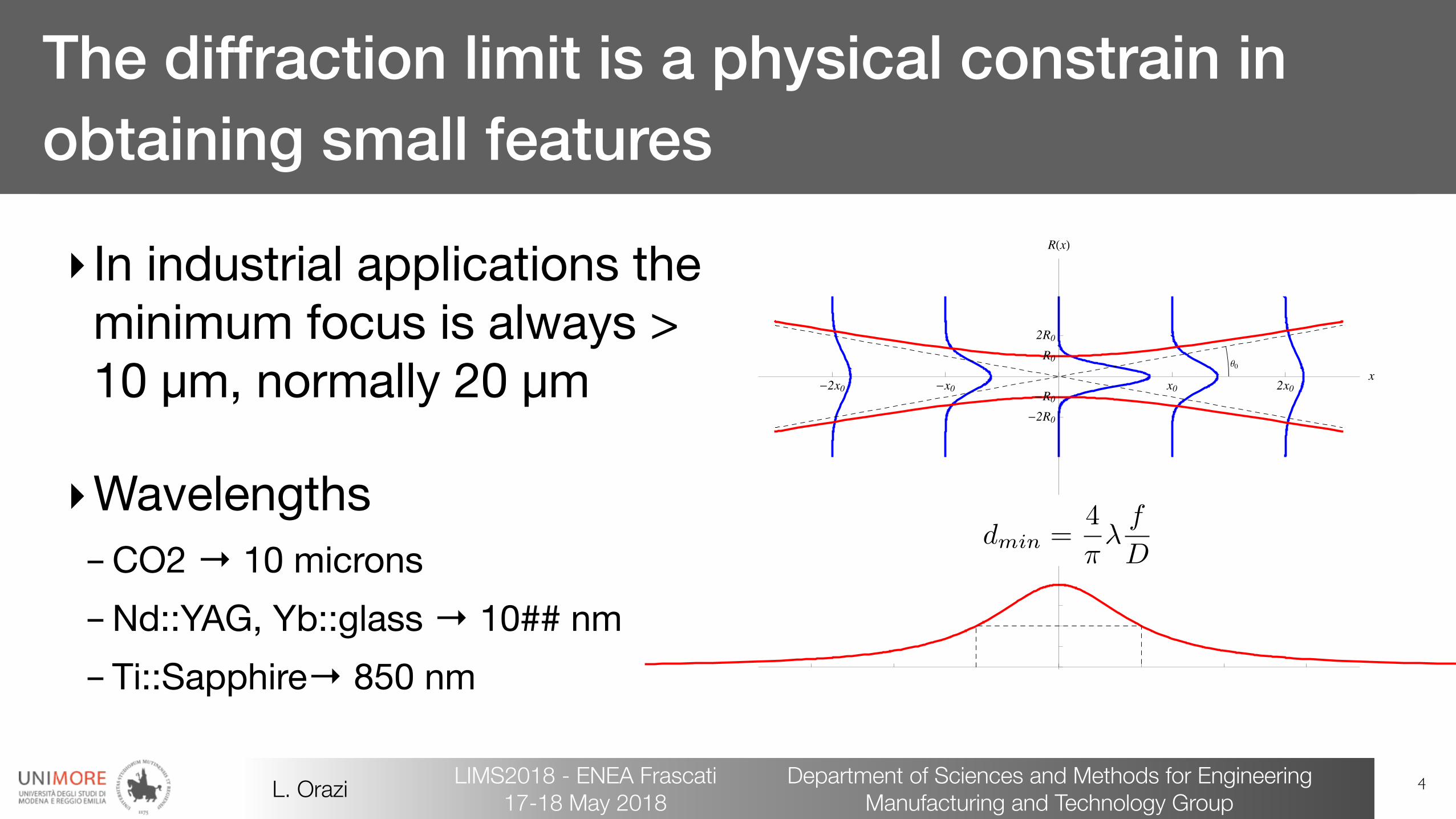
dmin =4
⇡�f
D
‣ In industrial applications the minimum focus is always > 10 µm, normally 20 µm
Laser Induced Periodic Surface Structures ( LIPPS )‣ First observed in dielectric in 1965‣ Role of self-organized dynamics has always
drawn interest.‣ LIPSS observed in metals, dielectrics,
semiconductors. Basic mechanism uncovered in 1980’s.
‣ Persistent difficulties with achieving fine control over the structures has limited impact of the field.
‣ Active field, with >1000 papers published, but few applications demonstrated so far.
• First observation in 1965.
• Role of self-organized dynamics has always drawn interest.
• LIPSS observed in metals, dielectrics, semiconductors.
• Basic mechanism uncovered in 1980’s.
• Persistent difficulties with achieving fine control over the
structures has limited impact of the field.
• Active field, with >1000 papers published, but few applicants
5Department of Sciences and Methods for Engineering Manufacturing and Technology Group
LIMS2018 - ENEA Frascati 17-18 May 2018L. Orazi
Audoard et al, 2010Guo et al, 2005
High Regular HR-LIPSS: electrodynamic theory
6Dipartimento di Scienze e Metodi dell’Ingegneria Tecnologia e Sistemi di Lavorazioni
LIMS2018 - ENEA Frascati 17-18 May 2018L. Orazi
Incoming high intensity laser pulse
Surface Plasmon-Polariton Wave:
modulation of the electron density
Electric field of the incident wave
interferes with the plasmonic field
Higher electric field ↓
stronger the electron heating
forming metal oxide (TiO2) of an amount that is proportional to thelaser-activated metal (titanium) or available O2 at that point, which-ever is smaller. Here, we simply refer to this controlled transformationas ablation, because similar physical processes underlie it, eventhough the metal is not removed, but is chemically transformed. Asa result of the ablation threshold, no processing of the surfaceshould occur between the nanolines, where partially destructive inter-ference leads to the total intensity being below the ablation threshold.The presence of this threshold, which was confirmed experimentally(Fig. 3; Supplementary Section ‘Experimental evidence for thethreshold for intensity’), is the main source of nonlinearity.
When scanning a small-diameter beam, the nanostructures arecreated sequentially, with existing structures creating new structures,similar to the toppling of dominoes. This enables the formation ofextremely uniform nanostructures (experimental and simulatedresults are shown in Fig. 3e and f, respectively). Moreover, it ispossible to tile indefinitely large areas with nanostructures,without a discernible reduction in long-range uniformity whenusing a small laser beam. We scan the beam along a line, thenshift the beam laterally while still preserving a partial overlap withthe previous point, and then scan again parallel to the line of thescan (with partial overlap being maintained all along the way withthe first line of the scan). This can be visually observed inSupplementary Movie S1, where the red disk represents the beamlocation and verified experimentally (Supplementary Movie S2).Further evidence of the role of nonlocal feedback lies in the factthat the new structures form a tilted front and the nanolinesbecome distorted into a wavy pattern at the end of each scan linedue to incomplete nonlocal feedback.
The nanostructure formation mechanism exhibits a significantdegree of robustness against distinct types of perturbations. First,the resultant field at any point is formed collectively by the entiresurrounding area, so the contributions of isolated defects or roughpatches on the surface are easily overwhelmed. When a defect isplaced along the beam path (under conditions otherwise the sameas in Fig. 3f), the nanolines suffer only minor distortions(Fig. 3g). Defects encountered in Supplementary Movie S2provide experimental confirmation. Second, Supplementary MovieS2 shows that the beam focus was not maintained well during scan-ning due to the poor mechanical stability of our set-up. However,key features, such as nanoline period and width, are independentof laser power (see Supplementary Section ‘Insensitivity of thenanostructure features to laser power and exposure time’ for directexperimental confirmation). Because of this insensitivity, a partialloss of focus during scanning is inconsequential. In fact, we foundthe standard and Allan deviations of the nanoline period of thisstructure to be 0.9 nm and 0.14 nm, respectively (for details seeSupplementary Section ‘Characterization of the uniformity of thenanostructures’). Third, as a result of the negative feedbackmechanism, the growth of the nanostructures saturates at a givenheight. Even minutes-long exposure to a stationary beam or multiplescans of the laser over the same area have no discernible effect(Supplementary Movie S4). Robustness against a range of pertur-bations is a coveted feature of nonlinear systems5 that is extremelydifficult to achieve in strictly linear systems.
A diverse range of nanostructures have been fabricated using thisapproach. A photograph of nanostructures covering a 3 mm2 area,fabricated on a thin and flexible glass slide, is presented in Fig. 4a.
0
10
0 200
10
0 50 100 150 200 250
40
0
10
0 50 100 150 200
x (µm)
0 20 40x (µm)
0 20 40x (µm)
y (µ
m)
e
f
g
0 40
4
8
0 100 200 300
8 0 40
4
8
0 50 100 150
8
a
b
c
d
Figure 3 | Nanostructure formation dynamics. a,b, SEM image of the experimental results (a) and numerical simulation results (b) of nanostructures formedaround an isolated scatterer by a few, high-energy pulses with linear polarization. c,d, SEM image of the experimental results (c) and numerical simulationresults (d) of nanostructures obtained with a large and stationary laser beam. e, SEM image of uniform nanostructures obtained by scanning a small laserbeam. f, Numerical simulation results of nanostructures obtained by scanning a small laser beam. g, Numerical simulation results showing robustness of thenanostructure formation against a defect, showing minor distortion and quick subsequent recovery. Colour bars indicate height in nanometres.
SUPPLEMENTARY INFORMATION DOI: 10.1038/NPHOTON.2013.272
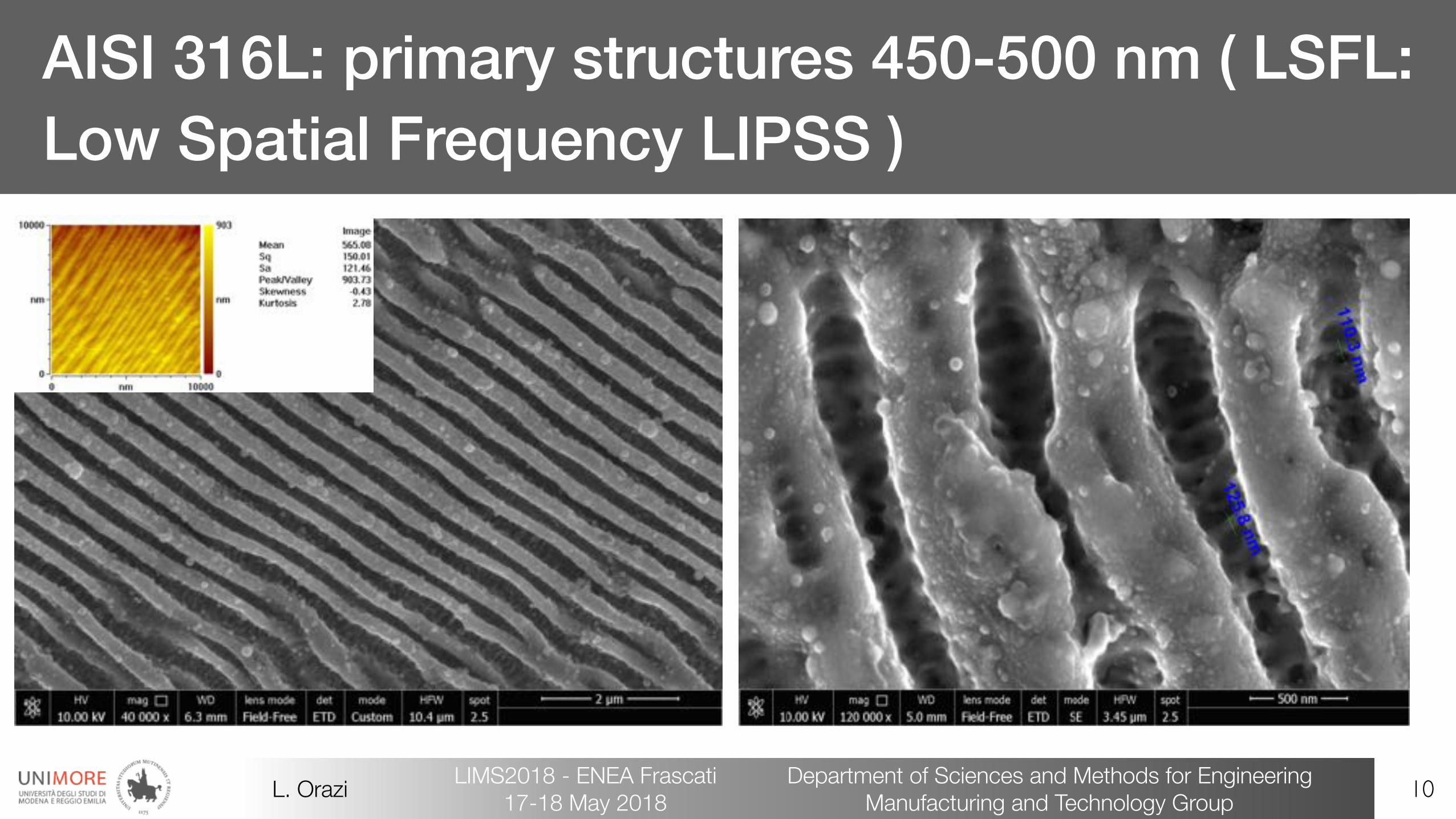
Nonlinear Laser Lithography: surface roughness and spot diameter are the key factors
7Dipartimento di Scienze e Metodi dell’Ingegneria Tecnologia e Sistemi di Lavorazioni
LIMS2018 - ENEA Frascati 17-18 May 2018L. Orazi
forming metal oxide (TiO2) of an amount that is proportional to thelaser-activated metal (titanium) or available O2 at that point, which-ever is smaller. Here, we simply refer to this controlled transformationas ablation, because similar physical processes underlie it, eventhough the metal is not removed, but is chemically transformed. Asa result of the ablation threshold, no processing of the surfaceshould occur between the nanolines, where partially destructive inter-ference leads to the total intensity being below the ablation threshold.The presence of this threshold, which was confirmed experimentally(Fig. 3; Supplementary Section ‘Experimental evidence for thethreshold for intensity’), is the main source of nonlinearity.
When scanning a small-diameter beam, the nanostructures arecreated sequentially, with existing structures creating new structures,similar to the toppling of dominoes. This enables the formation ofextremely uniform nanostructures (experimental and simulatedresults are shown in Fig. 3e and f, respectively). Moreover, it ispossible to tile indefinitely large areas with nanostructures,without a discernible reduction in long-range uniformity whenusing a small laser beam. We scan the beam along a line, thenshift the beam laterally while still preserving a partial overlap withthe previous point, and then scan again parallel to the line of thescan (with partial overlap being maintained all along the way withthe first line of the scan). This can be visually observed inSupplementary Movie S1, where the red disk represents the beamlocation and verified experimentally (Supplementary Movie S2).Further evidence of the role of nonlocal feedback lies in the factthat the new structures form a tilted front and the nanolinesbecome distorted into a wavy pattern at the end of each scan linedue to incomplete nonlocal feedback.
The nanostructure formation mechanism exhibits a significantdegree of robustness against distinct types of perturbations. First,the resultant field at any point is formed collectively by the entiresurrounding area, so the contributions of isolated defects or roughpatches on the surface are easily overwhelmed. When a defect isplaced along the beam path (under conditions otherwise the sameas in Fig. 3f), the nanolines suffer only minor distortions(Fig. 3g). Defects encountered in Supplementary Movie S2provide experimental confirmation. Second, Supplementary MovieS2 shows that the beam focus was not maintained well during scan-ning due to the poor mechanical stability of our set-up. However,key features, such as nanoline period and width, are independentof laser power (see Supplementary Section ‘Insensitivity of thenanostructure features to laser power and exposure time’ for directexperimental confirmation). Because of this insensitivity, a partialloss of focus during scanning is inconsequential. In fact, we foundthe standard and Allan deviations of the nanoline period of thisstructure to be 0.9 nm and 0.14 nm, respectively (for details seeSupplementary Section ‘Characterization of the uniformity of thenanostructures’). Third, as a result of the negative feedbackmechanism, the growth of the nanostructures saturates at a givenheight. Even minutes-long exposure to a stationary beam or multiplescans of the laser over the same area have no discernible effect(Supplementary Movie S4). Robustness against a range of pertur-bations is a coveted feature of nonlinear systems5 that is extremelydifficult to achieve in strictly linear systems.
A diverse range of nanostructures have been fabricated using thisapproach. A photograph of nanostructures covering a 3 mm2 area,fabricated on a thin and flexible glass slide, is presented in Fig. 4a.
0
10
0 200
10
0 50 100 150 200 250
40
0
10
0 50 100 150 200
x (µm)
0 20 40x (µm)
0 20 40x (µm)
y (µ
m)
e
f
g
0 40
4
8
0 100 200 300
8 0 40
4
8
0 50 100 150
8
a
b
c
d
Figure 3 | Nanostructure formation dynamics. a,b, SEM image of the experimental results (a) and numerical simulation results (b) of nanostructures formedaround an isolated scatterer by a few, high-energy pulses with linear polarization. c,d, SEM image of the experimental results (c) and numerical simulationresults (d) of nanostructures obtained with a large and stationary laser beam. e, SEM image of uniform nanostructures obtained by scanning a small laserbeam. f, Numerical simulation results of nanostructures obtained by scanning a small laser beam. g, Numerical simulation results showing robustness of thenanostructure formation against a defect, showing minor distortion and quick subsequent recovery. Colour bars indicate height in nanometres.
Figure 1. Laser-textured surfaces. Scanning electron microscopy micrographs and roughness profiles of laser-induced periodic surface structures (A–C), nanopillar- (D–F) and microcolumn- (G–I) textured surfaces. The arrows in (A, D & G) indicate the polarization direction of the laser beam. The micrographs in (B & E) were taken at a tilting angle of 45°. The scale bar is 5 μm (A & D), 10 μm (G) and 2 μm (B, E & H). LIPSS: Laser-induced periodic surface structure. For color figures, please see online at www.futuremedicine.com/doi/full/10.2217/NNM.15.19
future science group
Human mesenchymal stem cell behavior on femtosecond laser-textured Ti-6Al-4V surfaces Research Article
1–20 mm/s by means of a computer-controlled XYZ stage (PI miCos; Eschbach-Germany) while pulsing the laser at 1 kHz. To achieve complete surface cover-age, consecutive laser tracks were partially overlapped by a lateral displacement of about 30% of the track width. The polarization direction was controlled by a half-wave plate introduced in the optical path. The laser treatment was carried out in air.
(Ra) and maximum height (Rz), defined according to ISO 4287 standard and calculated from at least ten measurements taken from each stereoscopic pair in a direction perpendicular to the laser beam scanning direction.
The surface chemical composition was determined by x-ray photoelectron spectroscopy (XPS) using a XSAM800 (KRATOS) spectrometer operated in the fixed analyzer transmission mode, with a pass energy of 20 eV, nonmonochromatized AlKα radiation (hν = 1486.6 eV), 120 W power (10 mA × 12 kV) and a take-off angle relative to the surface holder of 45°. The samples were analyzed in ultra-high vacuum (∼10-7 Pa) at room temperature. The spectra were collected and stored in 300 channels with a step of 0.1 eV and 60 s of acquisition time by sweep, using Vision (KRA-TOS) software. The areas of the peaks components were evaluated after fitting with Gaussian-Lorentzian
Figure 3. Cell spreading. Low-magnification fluorescence images of human mesenchymal stem cells cultured on polished (A), laser-induced periodic surface structures (B), NPs (C) and microcolumn (D) surfaces 24 h after cell seeding. F-actin fibers (green) and cell nucleus (blue). The scale bar is 200 μm. Quantification of the cell area (E). *Statistically significant differences between the average values; p < 0.05. LIPSS: Laser-induced periodic surface structure; MC-LIPSS: Microcolumns covered with LIPSS; NP: Nanopillar.
70,000
56,000
42,000
28,000
14,000
0Polished LIPSSs MC-LIPSSsNPs
Culture substrates
Cel
l are
a (µ
m2 )
**
*
A B
C D
E
future science group
Research Article Cunha, Zouani, Plawinski et al.
the processing methods and parameters indicated in Table 1. The texture depicted in Figure 1A–C consists of nanoripples known as LIPSSs. The average period and the peak-to-valley distance are 715 ± 86 and 296 ± 58 nm, respectively. The second type of texture consists of an array of NPs (Figure 1D–F). The rounded tops of the NPs are due to resolidification of molten
material. The third type of texture consists of micro-columns with roughly elliptical cross-section covered with LIPSSs (Figure 1G–I), forming a bimodal surface roughness distribution. The length of the major and minor axis of the columns and their maximum height are 8 ± 2, 6 ± 1 and 4 ± 1 μm, respectively. These textures are not commensurate with the grain size of the material and bear no relationship with the mate-rial microstructure. The values of Ra and Rz for all the laser-textured surfaces are given in Table 2.
XPS survey spectra of the laser-treated surfaces are presented in Supplementary Figure 1 (see online at www.futuremedicine.com/doi/suppl/10.2217/nnm.15.19). They present peaks corresponding to titanium, alumi-num, oxygen and carbon, as well as Auger electrons peaks of Ti, O and C. The vanadium peaks are par-tially overlapped with the oxygen satellite peaks and cannot be distinguished. The Ti 2p, O 1s and Al 2p peaks are presented in Figure 2. The Ti 2p peak con-sists of three doublets with a spin-orbit split of 5.7 ± 0.1 eV. The main component (Ti 2p3/2) of the major dou-blet is centered at 458.3 ± 0.1 eV and can be assigned to Ti (IV) in TiO2. A less intense doublet with a Ti 2p3/2 component centered at 455.6 ± 0.2 eV can be assigned to Ti (III) in Ti2O3. In addition, for polished and nano-pillar textured specimens a third doublet with the Ti 2p3/2 component centered at 453.8 ± 0.2 eV is observed, which can be attributed to metallic titanium. The O 1s peak consists of three components at 529.9 ± 0.2, 531.5 ± 0.1 and 532.7 ± 0.3 eV. They can be attributed to O-2, a mixture of hydroxyl (OH-) and carbonyl groups (C = O) and oxygen singly bound to carbon (C – O), respectively. The presence of C – O and C = O groups was also confirmed by the analysis of the C 1s peak (not shown). The Al 2p peak consists of three doublets with a spin-orbit split of 0.4 eV. The most intense has its main component, Al 2p3/2, centered at 74.3 ± 0.1 eV and can be assigned to Al (III) in Al2O3. Another dou-blet, with the Al 2p3/2 component centered at 71.6 ± 0.1 eV, is observed for the polished surface and is due to metallic aluminum. Finally, a low-intensity doublet with the Al 2p3/2 component centered at 76.5 ± 0.1 eV is observed for microcolumn-textured surfaces, which
A. Cunha et al. - Human mesenchymal stem cell behavior on femtosecond laser-textured Ti-6Al-4V
surfaces. Nature - Nanomedicine. (2015)Can LIPSS improve the
osteointegration?
Ti/Zr alloys for bio-medical applications
25Department of Sciences and Methods for Engineering Manufacturing and Technology Group
LIMS2018 - ENEA Frascati 17-18 May 2018L. Orazi
30 lab rats divided in 4 groups
Laser nanopatterning
Dulbecco’s Modified Eagle Medium; Fetal Bovine Serum; L-glutamine; Mercaptoethanol24 h incubation 37 °C
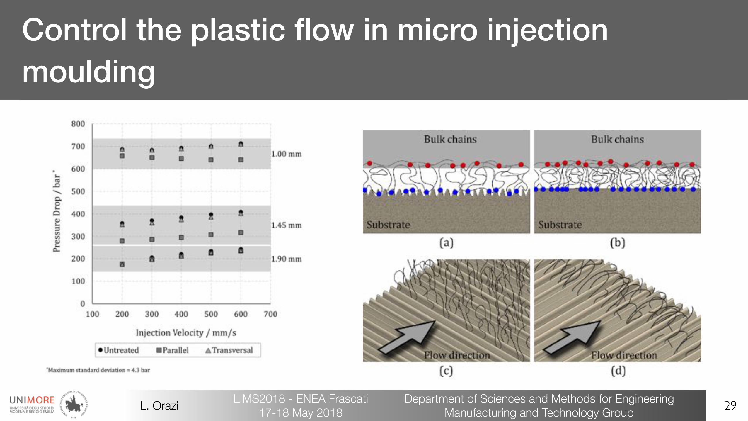
Control the plastic flow in micro injection moulding
‣Local treatments of mould surfaces in order to improve and control the plastic flow during injection.
28Department of Sciences and Methods for Engineering Manufacturing and Technology Group
LIMS2018 - ENEA Frascati 17-18 May 2018L. Orazi
21
+ -0,01
0,01
3 -00,01 7
-00,02
10
+ 0,04
0
A
A
superficial treatment
SEZIONE A-A
B
C
D
1 2
A
321 4
B
A
5 6
Codice disegno:
Titolo disegno: 37.COATED.FIXED.INSERTUniversità di PadovaDIMEG
Via Venezia, 135131 PADOVA
Rugosità gen: Scala 2:1
Quote senza indicazione di tolleranza:ISO 2768 - mK
DataFirma
Disegnato Controllato
Smussi non quotati: Racc. non quotati:
Materiale:A4
06/11/14
43 5 6
C
D
Control the plastic flow in micro injection moulding
29Department of Sciences and Methods for Engineering Manufacturing and Technology Group
LIMS2018 - ENEA Frascati 17-18 May 2018L. Orazi
Adhesive joint on Ti6Al4V alloy: improving of the shear maximum stress
30Department of Sciences and Methods for Engineering Manufacturing and Technology Group
LIMS2018 - ENEA Frascati 17-18 May 2018L. Orazi
E
Vs
F
E
Vs
F
Cutting Tools: generation of patterns for MoS2 deposits.
31Department of Sciences and Methods for Engineering Manufacturing and Technology Group
LIMS2018 - ENEA Frascati 17-18 May 2018L. Orazi
Silicon: PV applications
32Department of Sciences and Methods for Engineering Manufacturing and Technology Group
LIMS2018 - ENEA Frascati 17-18 May 2018L. Orazi
Sapphire: first results known in literature
‣Some first results on Sapphire
33Department of Sciences and Methods for Engineering Manufacturing and Technology Group
LIMS2018 - ENEA Frascati 17-18 May 2018L. Orazi
Diffraction effects: gratings with periodicity near the visible wavelength
34Department of Sciences and Methods for Engineering Manufacturing and Technology Group
LIMS2018 - ENEA Frascati 17-18 May 2018L. Orazi
Nickel
AISI 316 LTC
Diffraction effects: aesthetic and anti-counterfeiting applications
35Department of Sciences and Methods for Engineering Manufacturing and Technology Group
LIMS2018 - ENEA Frascati 17-18 May 2018L. Orazi
AISI 316 polishedAISI 316 unpolished
LIPSS@DISMI new set-up
‣3 harmonics laser‣Two concurrent
beamlines at 1030 and 343 nm with galvoscanner and laser spot ≈ 10!.‣XYZ stage +
polarization direction rotation
36Department of Sciences and Methods for Engineering Manufacturing and Technology Group
LIMS2018 - ENEA Frascati 17-18 May 2018L. Orazi
Bibliografia
[1] M. Sorgato, D. Masato, G. Lucchetta, and L. Orazi, “Effect of different laser-induced periodic surface structures on polymer slip in PET injection moulding,” CIRP Journal of Manufacturing Science and Technology, 2018.[2] I. Gnilitskyi, T. J.-Y. Derrien, Y. Levy, N. M. Bulgakova, T. Mocek, and L. Orazi, “High-speed manufacturing of highly regular femtosecond laser- induced periodic surface structures: physical origin of regularity,” Scientific Reports, vol. 7, p. 8485, Aug. 2017.[3] I. Gnilitskyi, A. Rota, R. Ctvrtlik, A. P. Serro, A. P. Serro, E. Gualtieri, and L. Orazi, “Multifunctional Properties of High-speed Highly Uniform Femtosecond Laser Patterning on Stainless steel,” in Conference on Lasers and Electro-Optics (2017), paper ATu1C.5, p. ATu1C.5, Optical Society of America, May 2017.[4] L. Orazi, I. Gnilitskyi, and A. P. Serro, “Laser Nanopatterning for Wet- tability Applications,” Journal of Micro and Nano-Manufacturing, vol. 5, pp. 021008–021008–8, Mar. 2017.[5] G. Rotella, L. Orazi, M. Alfano, S. Candamano, and I. Gnilitskyi, “Inno- vative high-speed femtosecond laser nano-patterning for improved adhesive bonding of Ti6al4v titanium alloy,” CIRP Journal of Manufacturing Sci- ence and Technology, 2017.[6] I. Gnilitskyi, V. Gruzdev, N. M. Bulgakova, T. Mocek, and L. Orazi, “Mechanisms of high-regularity periodic structuring of silicon surface by sub-MHz repetition rate ultrashort laser pulses,” Applied Physics Letters, vol. 109, p. 143101, Oct. 2016.[7] I. Gnilitskyi, S. Mamykin, M. Dusheyko, T. Borodinova, N. Maksimchuk, and L. Orazi, “Diffraction Gratings Prepared by HR-LIPSS for New Surface Plasmon-Polariton Photodetectors & Sensors,” in Frontiers in Optics 2016 (2016), paper JW4A.88, p. JW4A.88, Optical Society of America, Oct. 2016.[8] I. Gnilitskyi, L. Orazi, N. Bulgakova, and V. Gruzdev, “Formation and Application of highly-regular LIPSS on Surface of Silicon Crystals,” in Frontiers in Optics 2016 (2016), paper JTh2A.113, p. JTh2A.113, Optical Society of America, Oct. 2016.
[9] I. Gnilitskyi, F. Rotundo, C. Martini, I. Pavlov, S. Ilday, E. Vovk, F. O . Ilday, and L. Orazi, “Nano patterning of AISI 316l stainless steel with Non- linear Laser Lithography: Sliding under dry and oil-lubricated conditions,” Tribology International, vol. 99, pp. 67–76, July 2016.[10] I. Gnilitskyi, L. Orazi, N. Bulgakova, and V. Gruzdev, “Highly Regular Nanostructuring of Si Surface by Ultrashort Laser Pulses,” in Conferenceon Lasers and Electro-Optics (2016), paper STh1Q.4, p. STh1Q.4, Optical Society of America, June 2016.[11] I. Gnilitskyi, M. Pogorielov, D. Dobrota, R. Viter, L. Orazi, and O. Mis- chenko, “Cell and Tissue Response to Modified by Laser-induced Periodic Surface Structures Biocompatible Materials for Dental Implants,” in Con- ference on Lasers and Electro-Optics (2016), paper AW4O.6, p. AW4O.6, Optical Society of America, June 2016.[12] I. Gnilitskyi, M. Dusheyko, T. Borodinova, S. Mamykin, N. Maksim- chuk, A. Ivaschuk, Y. Yakymenko, and L. Orazi, “Self-assembling of Gold Nanoparticles on Si-based Laser Nanotextured 1d Surface for Plasmonic Application,” in Conference on Lasers and Electro-Optics (2016), paper STh4K.3, p. STh4K.3, Optical Society of America, June 2016.[13] L. Orazi, I. Gnilitskyi, I. Pavlov, A. P. Serro, S. Ilday, and F. O. Ilday, “Nonlinear laser lithography to control surface properties of stainless steel,” CIRP Annals - Manufacturing Technology, vol. 64, no. 1, pp. 193–196, 2015.[14] I. Gnilitskyi, I. Pavlov, F. Rotundo, L. Orazi, C. Martini, and F. Ilday, “Nonlinear laser lithography for enhanced tribological properties,” in Con- ference on Lasers and Electro-Optics Europe - Technical Digest, vol. 2015- August, Institute of Electrical and Electronics Engineers Inc., 2015.[15] I. Gnilitskyi, I. Pavlov, F. Rotundo, L. Orazi, S. Ilday, C. Martini, and F. Ilday, “Laser-patterning stainless steel with nonlinear laser lithography for enhanced tribological properties,” vol. Part F4-CLEO 2015, 2015.
37Department of Sciences and Methods for Engineering Manufacturing and Technology Group
LIMS2018 - ENEA Frascati 17-18 May 2018L. Orazi
Laser Induced Periodic Surface Structures: from physical phenomena to