28
Laser Link ® III 1310 nm Modular Optical Transmitter 45-870 MHz Installation Booklet Part Number 711970001

Laser Link® III1310 nm ModularOptical Transmitter45-870 MHzInstallation BookletPart Number 711970001

Please read this entire guideVeuillez lire entièrement ce guideBitte das gesamte Handbuch durchlesenSirvase leer completamente la presente guíaSi prega di leggere completamente questa guida
Important
Please read this entire guide before you install or operate this product. Giveparticular attention to all safety statements.
Important
Veuillez lire entièrement ce guide avant d’installer ou d’utiliser ce produit.Prêtez une attention particulière à toutes les règles de sécurité.
Zu beachten
Bitte lesen Sie vor Aufstellen oder Inbetriebnahme des Gerätes diesesHandbuch in seiner Gesamtheit durch. Achten Sie dabei besonders auf dieSicherheitshinweise.
Importante
Sírvase leer la presente guía antes de instalar o emplear este producto. Presteespecial atención a todas los avisos de seguridad.
Importante
Prima di installare o usare questo prodotto si prega di leggere completamentequesta guida, facendo particolare attenzione a tutte le dichiarazioni disicurezza.

Laser Link® III1310 nm ModularOptical Transmitter45-870 MHz
Installation Booklet
Part Number 711970001

©2000 by ANTEC CorporationAll rights reserved.No part of this book may be reproducedin any form or by any means, withoutpermission in writing fromANTEC Corporation.
Publication Date – May 19, 2000
Data, drawings, and other materialcontained herein are proprietary toANTEC Corporation and may not bereproduced or duplicated in any form without the prior permission ofANTEC Corporation.
When ordering parts fromANTEC Network Technologies , be sureto include the equipment model number,equipment serial number, and adescription of the part.
In all correspondence with ANTECCorporation regarding this publication,refer to:
711970001May 19, 2000
ANTEC Network Technologies is a divisionand trademark of ANTEC Corporation.
711970001 Laser Link III 1310 nm Transmitter Installation Booklet 1-1
Chapter 1General Information
Overview
Introduction This manual describes the installation and operation of the Laser Link III 1310 nmModular Optical Transmitter (1310 nm Transmitter).
ManualContents
This manual contains three chapters.
• Chapter 1 – General Information• Chapter 2 – Installation• Chapter 3 – Activating the 1310 nm Transmitter
How to Con-tact ANTECNetworkTechnologies
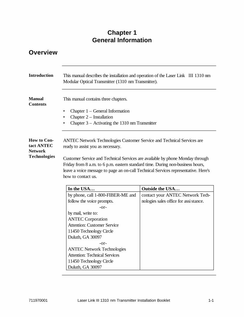
ANTEC Network Technologies Customer Service and Technical Services areready to assist you as necessary.
Customer Service and Technical Services are available by phone Monday throughFriday from 8 a.m. to 6 p.m. eastern standard time. During non-business hours,leave a voice message to page an on-call Technical Services representative. Here'show to contact us.
In the USA… Outside the USA…by phone, call 1-800-FIBER-ME andfollow the voice prompts.
-or-by mail, write to:ANTEC CorporationAttention: Customer Service11450 Technology CircleDuluth, GA 30097
-or-ANTEC Network TechnologiesAttention: Technical Services11450 Technology CircleDuluth, GA 30097
contact your ANTEC Network Tech-nologies sales office for assi stance.

Chapter 1 – General Information
1-2 Laser Link III 1310 nm Transmitter Installation Booklet 711970001
Safety
Overview Safety of personnel is the primary concern during all procedures. Refer to the Laser Link III 1310 nm Modular Optical Transmitter Installation and OperationManual for complete safety info rmation.
Labels A safety label is affixed to this equipment in plain view. The safety label is shownbelow.
ANTEC Network Technologies 11450 Technology CircleDuluth, GA 30097 U.S.A
ATTENTION Observe precautions for
handling electrostatic sensitive devices
Invisible laser radiation - Avoid exposure to Beam. MAX. output power: Wavelength: 1310 nm Refer to user's manual. This product complies with IEC 825-1, 1993 as a laser product. Class
Invisible laser radiation - Avoid direct exposure to beam. Operate only with proper optical fiber installed in connector. Refer to user's manual. This product complies with 21 CFR 1040.10. FDA - Class 1
S/N:
Manufactured: Month Year
Manufacturing Site
DANGER
1
xxxxxxxxxxxxxxxx

Chapter 1 – General Information
711970001 Laser Link III 1310 nm Transmitter Installation Booklet 1-3
Equipment Description
Overview The 1310 nm Transmitter family is composed of a tiered series of 1310 nm fiberoptic transmitters that allow for targeted carrier-to-noise and distortion perform-ance over varied loss budgets. The low power versions of the product are designedfor delivery of targeted services such as voice, data and video on demand.
The medium and high power products fit into broader area and longer link budgetapplications such as headend consolidations.
Product features are provided in the following table.
Product FeatureFront Panel Ac-cessible TestPoints
• Optical Output Power1 V dc/10 mW
• Laser Drive Level(labeled RF Test)10 dBmV/channel at 110 channel NTSC i nput
Front Panel Ac-cessible Con-trols
• Power On/Off (Laser Enable)Latching type switch
• Slope0-5 dB, 45-870 MHz
• Attenuation Adjust±2 dB min.
Front Panel Ac-cessibleIndicators
• Green/Red POWER LED• Green/Red/(Amber, if applicable) TEMP/FAN LED• Green/Red OPT PWR LED• Green/Red BIAS LED
Front PanelAccessible Op-ticalInterface
• SC/UPC• SC/APC• E2000
Monitoring andControl
• Compatible with either Laser Link Mainframe III or II
Continued on next page
Chapter 1 – General Information
1-4 Laser Link III 1310 nm Transmitter Installation Booklet 711970001
Equipment Description, Continued
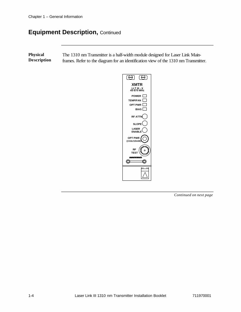
PhysicalDescription
The 1310 nm Transmitter is a half-width module designed for Laser Link Mai n-frames. Refer to the diagram for an identification view of the 1310 nm Transmitter.
XMTR
RF ATTN
SLOPE
OPT PWR(1Vdc/10mW)
LASER ENABLE
RFTEST
LLT III - X45-870 MHz
POWER
TEMP/FAN
OPT PWR
BIAS
Continued on next page
Chapter 1 – General Information
711970001 Laser Link III 1310 nm Transmitter Installation Booklet 1-5
Equipment Description, Continued
FunctionalDescription
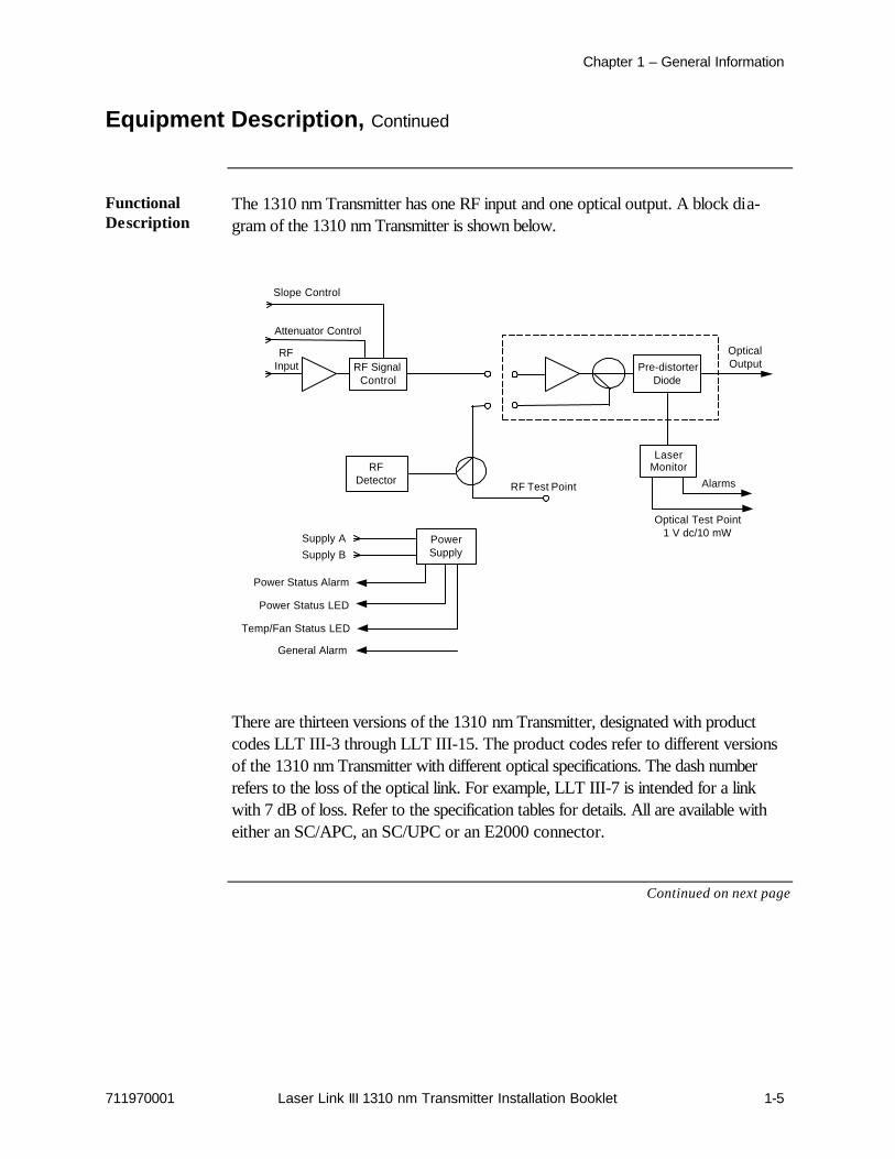
The 1310 nm Transmitter has one RF input and one optical output. A block dia-gram of the 1310 nm Transmitter is shown below.
Slope Control
Attenuator Control
RFInput
Supply A
General Alarm
Temp/Fan Status LED
Power Status LED
Power Status Alarm
PowerSupplySupply B
RF Test Point
RFDetector
RF SignalControl
OpticalOutputPre-distorter
Diode
Alarms
Optical Test Point1 V dc/10 mW
LaserMonitor
There are thirteen versions of the 1310 nm Transmitter, designated with productcodes LLT III-3 through LLT III-15. The product codes refer to different versionsof the 1310 nm Transmitter with different optical specifications. The dash numberrefers to the loss of the optical link. For example, LLT III-7 is intended for a linkwith 7 dB of loss. Refer to the specification tables for details. All are available witheither an SC/APC, an SC/UPC or an E2000 connector.
Continued on next page

Chapter 1 – General Information
1-6 Laser Link III 1310 nm Transmitter Installation Booklet 711970001
Equipment Description, Continued
Functional Description (continued)
RF input levels vary according to model and channel loading.
ModelChannelLoading RF Input
79 13 to 17 dBmV/ch96 12.25 to 16.25 dBmV/chLLT III-3 through LLT III-12112 11.5 to 15.5 dBmV/ch
Note: For models LLT III-13 and up, required power is increased by 1 dBmV/ ch.
Optimum RF drive level varies from diode to diode, even between identical pro d-ucts. The RF test point is provided to enable the user to optimize the product per-formance. This test point is calibrated to provide 10 dBmV/ch when the inputpower is at the optimal level (110 NTSC channels). This level is 11.5 dBmV/channel with a reduced load of 79 NTSC cha nnels.
The 1310 nm Transmitter also provides power alarms and status indications to theLaser Link user panel or the Element Management Interface Card (EMIC). In either case, the 1310 nm Transmitter provides information through the mainframegeneral operational alarm (GOALN). The ALARM LED on the user panel orEMIC will illuminate red if any of the following occur with the 1310 nm Transmitter:
• Redundant power supply is selected• Optical output power drops by 25%• Laser temperature is out of range• Laser bias is out of range• Fan has failed (if amber indicator exists, LED will illuminate amber)
If employed, the Laser Link EMIC collects the vital signs signals from the modulesin the Laser Link Mainframe. The EMIC is the communications link between theLaser Link Mainframe and the Track Link Element Management System.

Chapter 1 – General Information
711970001 Laser Link III 1310 nm Transmitter Installation Booklet 1-7
Equipment Specifications
Overview This section describes specifications of the 1310 nm Transmitter.
OpticalSpecifications
The tables below list optical specifications.
Characteristic SpecificationOutput Power See table belowConnector Return Loss >65 dB SC/APC
>55 dB SC/UPC>65 dB E2000
Wavelength 1310 ±20 nm
Model
OutputPowerdBm Total Optical Loss (dB)
1 2 3 4 5 6 7 8 9 10 11 12 13 14 15 16 17CNR (dB)
LLT III-3 2-4 55 54 53 52 51LLT III-4 3-5 55 54 53 52 51LLT III-5 4-6 55 54 53 52 51LLT III-6 5-7 55 54 53 52 51LLT III-7 6-8 55 54 53 52 51LLT III-8 7-9 55 54 53 52 51LLT III-9 8-10 54.5 53.5 52.5 51.5 50.5LLT III-10 9-11 54.5 53.5 52.5 51.5 50.5LLT III-11 10-12 54.5 53.5 52.5 51.5 50.5LLT III-12 11-13 54 53 52 51 50LLT III-13 12-14 54 53 52 51 50LLT III-14 12-15 54 53 52 51 50LLT III-15 13-16 54 53 52 51 50
Notes:• CTB = -70 dBc• CSO = -65 dBc• Total path loss equals 0.5 dB passive connector loss with the balance of all fiber loss at
0.35 dB/km.• Referenced load is 79 NTSC channels.• Performance measured in accordance with NCTA practices using unmod ulated CW
carriers.
Continued on next page

Chapter 1 – General Information
1-8 Laser Link III 1310 nm Transmitter Installation Booklet 711970001
Equipment Specifications, Continued
RFSpecifications
The table below lists RF specifications.
Characteristic SpecificationRF Bandwidth 45-870 MHzRF Frequency Response ± 0.75 dBRF Input Return Loss ≥17 dB (45 to 550 MHz)
≥15 dB (550 to 870 MHz)RF Input Impedance 75 OhmsRF Input Level (signal requirre-ment for 79-channel loading)
Series 3 through 12: 15 dBmV/channelSeries 13 and up: 16 dBmV/channel
RF Input Connector Type F, 75-Ohm
PowerSpecifications
The table below lists power specifications.
Characteristic SpecificationInput Power +24 V dc provided by Laser
Link MainframePower Consumption 24 W maximum
PhysicalSpecifications
The table below lists physical specifications.
Characteristic SpecificationOperating Temperature -4 to 150 ºF (-20 to 65 ºC)Storage Temperature -6.2 to +156°F
(-40 to +70°C)Relative Humidity 5 to 95%, noncondensingMounting Requires Laser Link MainframeDimensions
HeightWidthDepth
5.25 in (13.3 cm)1.07 in (2.72 cm)13.5 in (34.3 cm)
**END OF CHAPTER**

711970001 Laser Link III 1310 nm Transmitter Installation Booklet 2-1
Chapter 2Installation
Overview
Introduction This chapter describes installation of the Laser Link III 1310 nm Modular OpticalTransmitter (1310 nm Transmitter).
Unpacking ANTEC Network Technologies thoroughly inspects and carefully packs all equi p-ment before shipment. At the time of shipment, the carrier assumes responsibility forits safe delivery; therefore, do not return damaged units to ANTEC Network Tech-nologies.
Procedure Unpack the transmitter according to the procedure below.
Step Action1 Inspect shipping carton for visible damage.2 Open the shipping carton. Retain shipping carton(s) until installation is
complete.3 Remove all packing material.4 Inspect unit for visible damage.5 Using packing list, check for missing items.

Chapter 2 - Installation
2-2 Laser Link III 1310 nm Transmitter Installation Booklet 711970001
Overview, Continued
Inspection Follow this procedure to inspect the 1310 nm Transmitter.
What to doabout VisibleDamage
Report visible damage as follows.
NOTE
Failure to adequately describe visible damage may result in the carrier refusing to honor a damage claim. The carrier will supply therequired form for filing such a claim.
Step Action1 Obtain a claim form from the carrier.2 Make a note of any visible damage on the freight bill or re ceipt.3 Have freight bill or receipt signed by the carrier's agent.
What to doaboutConcealedDamage
Concealed damage is not apparent until after unpacking. The contents may bedamaged in transit due to rough handling even though the carton may not show external damage. The carrier is responsible for hidden damage caused in transit. If youfollow these instructions carefully, ANTEC Corporation (ANTEC) guarantees itsfull support of your claims to protect you against loss from concealed da mage.
Step Action1 If you discover damage after unpacking, make a written request for i n-
spection by the carrier's agent within 15 days of delivery date.2 File any claims with the carrier’s agent, not ANTEC Network Technolo-
gies.
Continued on next page

Chapter 2 - Installation
711970001 Laser Link III 1310 nm Transmitter Installation Booklet 2-3
Overview, Continued
How toInventoryEquipment
Follow this procedure to inventory equipment.
Step Action1 Check off each item received against the list on the packing slip included
with the shipment.2 Verify this list matches the purchase order.3 If any items are missing, contact ANTEC Network Technologies.
In the USA… Outside the USACall 1-800-FIBER-ME andfollow the voice prompts.
Contact your ANTEC NetworkTechnologies sales office forassistance.
4 Return a copy of the packing slip with the missing item(s) circled.
How to ReturnEquipment
ANTEC Network Technologies makes every effort to ensure parts and equipmentarrive in working condition. Occasionally, it may be necessary to return parts orequipment that are not in working condition.
Procedure Follow this procedure to return equipment.
Step Action1 Contact ANTEC Network Technologies Technical Services to request
a Return for Repair (RR) number.
In the USA… Outside the USA…call 1-800-FIBER-ME and fol-low the voice prompts.
contact your ANTEC NetworkTechnologies sales office forassistance.
2 Tag or otherwise identify the defective equipment. Be sure to write theRR number on the tag.
3 If possible, reference the sales order, purchase order, and the date theequipment was received.
Continued on next page

Chapter 2 - Installation
2-4 Laser Link III 1310 nm Transmitter Installation Booklet 711970001
Overview, Continued
Procedure (continued)
Step Action4
CAUTION
Do not use Styrofoam chips (peanuts). Use of Sty-rofoam chips will void the warranty.
Pack the equipment in the original container and protective packingmaterial, if possible. If the original packing material is not available, usea sturdy corrugated box and appropriate packing material.
5 Include the following information:
Your NameCompany NameStreet AddressCity, State, Country and Zip/Postal CodeTelephone NumberRR NumberProblem Description
6 Ship equipment as directed by ANTEC Network Technologies Tec h-nical Services.
NOTE
ANTEC Network Technologies will not accept freightthat is shipped collect. Be sure to ship all items prepaid.

Chapter 2 - Installation
711970001 Laser Link III 1310 nm Transmitter Installation Booklet 2-5
Installation
Overview This section describes installing the 1310 nm Transmitter.
The 1310 nm Transmitter is shipped assembled. The applicable shielded cable assembly is included.
Install the 1310 nm Transmitter in any slot, 1 through 14, of the mainframe. Afterinstallation, refer to the procedures in Chapter 3, Activating the1310 nm Transmitter, to activate the 1310 nm Transmitter.
Procedure Follow this procedure to install the 1310 nm Transmitter. Note that the RF inputcable is not installed in this procedure. Do not install the RF input cable until youperform the setup procedure in chapter 3.
Step Action1
CAUTION
Static sensitive devices. Always wear a properlygrounded wrist strap when working on this equip-ment. The shelf has a grounding jack that may beused to plug in the wrist strap. Failure to observethis caution may result in equipment damage orpremature equipment failure.
Open the front cover of the mainframe by turning the front panel latchhandles counterclockwise.
2 Carefully insert the transmitter into an empty slot of the Laser LinkMainframe. Align the flange on the top and bottom of the module withthe top and bottom slide rail on the mainframe.
3 Secure the transmitter in the shelf with the two captive screws locatedon the top of the transmitter front faceplate. The screws are providedwith the module.
4 Locate the bulkhead optical connector on the front panel. Clean theconnector.
Continued on next page

Chapter 2 - Installation
2-6 Laser Link III 1310 nm Transmitter Installation Booklet 711970001
Installation, Continued
Procedure (continued)
Step Action5 Determine in which mainframe the 1310 nm Transmitter is being i n-
stalled.If… Then…Laser Link II Mainframe go to Step 6.Laser Link III Mainframe go to Step 7.
6 For a Laser Link II Mainframe, connect a 26 to 15-pin D-type shieldedcable adapter assembly by following the steps below.
Step Action1 On the rear of the module connect the 26-pin end to
the connector labeled POWER by depressing the sidetabs of the quick release latch mechanism.
2 Connect the 15-pin end to the connector on thepower distribution board of the mainframe that corre-sponds to the module slot J1A-J7B (half-widthmodular bays). Secure the connector with screws.
7 For a Laser Link III Mainframe, connect a 26 to 26-pin D-typeshielded cable adapter assembly by following the steps below.
Step Action1 On the rear of the module connect the smaller
26-pin end to the connector labeled POWER by de-pressing the side tabs of the quick release latchmechanism.
2 Connect the other 26-pin end to the connector on thepower distribution board of the mainframe that corre-sponds to the module slot, J1A-J7B (half-widthmodular bays). Secure the connector with screws.
Continued on next page

Chapter 2 - Installation
711970001 Laser Link III 1310 nm Transmitter Installation Booklet 2-7
Installation, Continued
Procedure (continued)
Step Action8 Verify mainframe power is on and press recessed latching switch
(LASER ENABLE) to activate the 1310 nm Transmitter.9 Verify that the POWER, TEMP/FAN, OPT PWR and BIAS LEDs
are green before proceeding. Note that while the 1310 nm Transmitteris stabilizing during initial startup, the LEDs may be red.
10 Press recessed latching switch (LASER ENABLE) to deactivate the1310 nm Transmitter.
11 Clean outgoing fiber connector.12
NOTE
Do not connect the RF input cable yet.
Connect the 1310 nm Transmitter to the outgoing fiber connector.13 Continue to chapter 3 to activate the 1310 nm Transmitter.

Chapter 2 - Installation
2-8 Laser Link III 1310 nm Transmitter Installation Booklet 711970001
(This page intentionally blank.)
**END OF CHAPTER**

711970001 Laser Link III 1310 nm Transmitter Installation Booklet 3-1
Chapter 3Activating the 1310 nm Transmitter
Overview
Introduction This chapter describes how to activate the Laser Link III 1310 nm Modular Opti-cal Transmitter (1310 nm Transmitter). Activation consists of connecting the RFinput signal to the 1310 nm Transmitter. These procedures assume the 1310 nmTransmitter is installed according to the procedures in chapter 2 of this ma nual.
RF SignalInput Check
Check the RF input signal with a spectrum analyzer prior to connecting the cable tothe RF input connector of the module. In the case of a 79 NTSC channel load, thelaser drive level has been optimized during manufacture to achieve the specified linkperformance of the module with an RF input level of:
• 15 dBmV/channel (LLT III-3 through LLT III-12)• 16 dBmV/channel (LLT III-13 through LLT III-15)
The optimized RF test port output value is 11.5 dBmV/channel for 79-channelloading and 10 dBmV/channel for 110-channel loading.
Procedure Connect the cable according to the following procedure.
Step Action1 Verify the correct RF level.2 Connect the 75-Ohm cable to the RF input port on the rear of the
1310 nm Transmitter.
Continued on next page

Chapter 3 – Activating the 1310 nm Transmitter
3-2 Laser Link III 1310 nm Transmitter Installation Booklet 711970001
Overview, Continued
RF SignalInput Slope
Due to the characteristic attenuation of the cable normally used between theheadend combiner network and the optical transmission equipment, a sloped RFinput is often obtained. The 1310 nm Transmitter module is designed to compe n-sate for 5 dB of cable loss (approximately 100 feet).
Procedure If a tilt is present, adjust the highest utilized frequency 's RF level to the proper levelshown in the RF signal input diagram.
Connect the spectrum analyzer according to the following procedure.
Step Action1 Connect the spectrum analyzer to the RF test point on the front of the
laser.2 Using a spectrum analyzer, set a display line to establish a reference on
the highest frequency carrier.3 Adjust the front panel gain control in order that the highest frequency
carrier is at the proper level (11.5 dBmV for 79 NTSC channels).4 Adjust the slope control to obtain a flat response at the desired level
across the channel bandwith.5 Record the RF test point level for future reference and routine maint e-
nance.
Continued on next page

Chapter 3 - Activating the 1310 nm Transmitter
711970001 Laser Link III 1310 nm Transmitter Installation Booklet 3-3
Overview, Continued
Operation withReducedChannel Load
The RF input level to the 1310 nm Transmitter can be increased with a reducedchannel load to take advantage of an improved carrier-to-noise ratio (CNR). Thisis often desirable in supertrunk applications using split band operation. The drivelevel is increased by 10 log (79/x) where x is equal to the desired channel load. TheCNR is improved by approximately the same factor. Refer to the RF signal inputdiagram to help determine the appropriate input level to the 1310 nm Transmitter.
RF SignalInput Diagram
18.017.5
17.016.516.0
15.5
15.0
14.514.0
13.5
13.0
40 50 60 70 80 90 100 110
Operation withIncreasedChannel Load
For operation above 79 channels, it is necessary to reduce the input level to the1310 nm Transmitter to maintain the appropriate headroom below the clippingpoint of the laser. The reduction in level is again derived from 10 log (79/x) where xis equal to the desired channel load. Refer to the RF signal i nput diagram.

Chapter 3 – Activating the 1310 nm Transmitter
3-4 Laser Link III 1310 nm Transmitter Installation Booklet 711970001
Controls and Indicators
Introduction This section describes the controls and indicators of the 1310 nm Transmitter.
Front PanelControls andIndicators
The front panel of the 1310 nm Transmitter provides access to the optical and RFtest points, the RF attenuator and slope adjustment, the LED diagnostic indicators,the laser enable switch and the optical output connector.
Diagram This diagram shows the front panel of the 1310 nm Transmitter.
XMTR
RF ATTN
SLOPE
OPT PWR(1Vdc/10mW)
LASER ENABLE
RFTEST
LLT III - X45-870 MHz
POWER
TEMP/FAN
OPT PWR
BIAS
1
2
3
4
5
6
7
8
9
10
Continued on next page
Chapter 3 - Activating the 1310 nm Transmitter
711970001 Laser Link III 1310 nm Transmitter Installation Booklet 3-5
Controls and Indicators, Continued
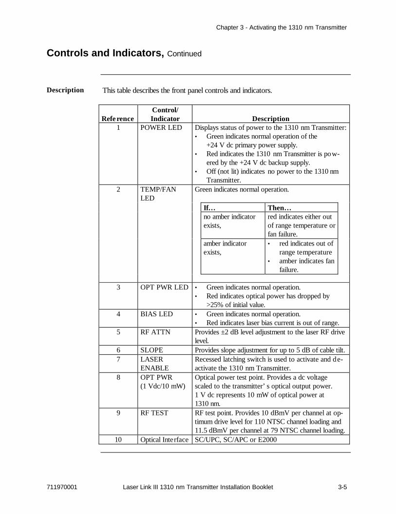
Description This table describes the front panel controls and indicators.
Refe renceControl/Indicator Description
1 POWER LED Displays status of power to the 1310 nm Transmitter:• Green indicates normal operation of the
+24 V dc primary power supply.• Red indicates the 1310 nm Transmitter is pow-
ered by the +24 V dc backup supply.• Off (not lit) indicates no power to the 1310 nm
Transmitter.2 TEMP/FAN
LEDGreen indicates normal operation.
If… Then…no amber indicatorexists,
red indicates either outof range temperature orfan failure.
amber indicatorexists,
• red indicates out ofrange temperature
• amber indicates fanfailure.
3 OPT PWR LED • Green indicates normal operation.• Red indicates optical power has dropped by
>25% of initial value.4 BIAS LED • Green indicates normal operation.
• Red indicates laser bias current is out of range.5 RF ATTN Provides ±2 dB level adjustment to the laser RF drive
level.6 SLOPE Provides slope adjustment for up to 5 dB of cable tilt.7 LASER
ENABLERecessed latching switch is used to activate and de-activate the 1310 nm Transmitter.
8 OPT PWR(1 Vdc/10 mW)
Optical power test point. Provides a dc voltagescaled to the transmitter’s optical output power.1 V dc represents 10 mW of optical power at1310 nm.
9 RF TEST RF test point. Provides 10 dBmV per channel at op-timum drive level for 110 NTSC channel loading and11.5 dBmV per channel at 79 NTSC channel loading.
10 Optical Interface SC/UPC, SC/APC or E2000
Chapter 3 – Activating the 1310 nm Transmitter
3-6 Laser Link III 1310 nm Transmitter Installation Booklet 711970001
Controls and Indicators, Continued
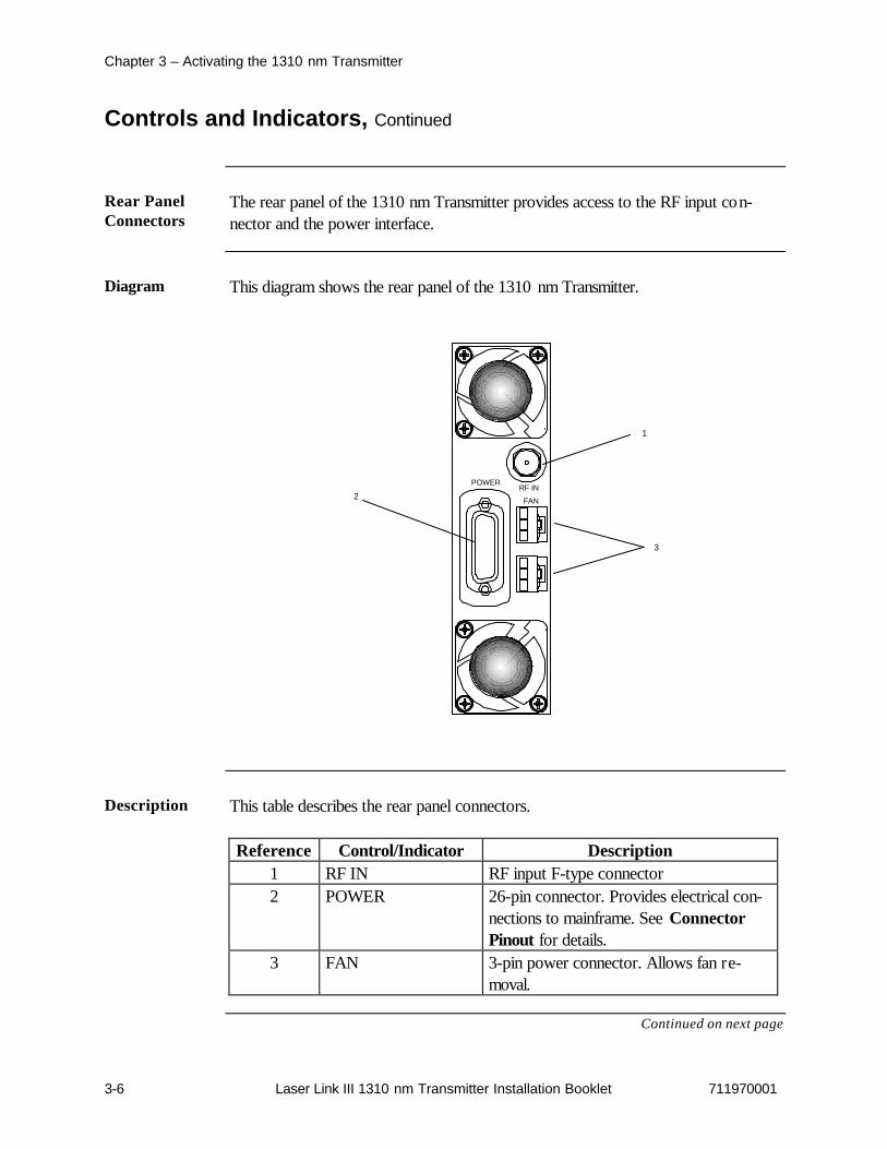
Rear PanelConnectors
The rear panel of the 1310 nm Transmitter provides access to the RF input con-nector and the power interface.
Diagram This diagram shows the rear panel of the 1310 nm Transmitter.
1
2
3
POWERRF IN
FAN
Description This table describes the rear panel connectors.
Reference Control/Indicator Description1 RF IN RF input F-type connector2 POWER 26-pin connector. Provides electrical con-
nections to mainframe. See ConnectorPinout for details.
3 FAN 3-pin power connector. Allows fan re-moval.
Continued on next page

Chapter 3 - Activating the 1310 nm Transmitter
711970001 Laser Link III 1310 nm Transmitter Installation Booklet 3-7
Controls and Indicators, Continued
ConnectorPinout
• Use the 26- to 26-pin cable on the Laser Link III Mainframe.• Use the 26- to 15-pin cable on the Laser Link II Mainframe.
Module26-Pin Mini D Ribbon
Laser Link III Mainframe26-Pin Dense D
Laser Link II Mainframe15-Pin Regular D
Pin Signal Pin Signal Pin SignalP1-1 GND P2-1 GND P2-1 GNDP1-2 GND P2-9 GND P2-8 GNDP1-3 +24 V dc, A P2-8 +24 V dc, A P2-6 +24 V dc, AP1-4 +24 V dc, A P2-17 +24 V dc, A P2-14 +24 V dc, AP1-5 Global Alarm P2-7 Global Alarm P2-4 Global AlarmP1-6 Spare 1 P2-3 Spare 1 P2-2 Spare 1P1-7 Laser Bias Current P2-6 Laser Bias Current P2-12 Laser Bias CurrentP1-8 Spare 2 P2-4 Spare 2 P2-3 Spare 2P1-9 Optl output power P2-5 Optl output power P2-11 Optl output powerP1-10 +24 V dc, B P2-2 +24 V dc, B P2-7 +24 V dc, BP1-11 +24 V dc, B P2-11 +24 V dc, BP1-12 GND P2-10 GND P2-15 GNDP1-13 GND P2-18 GNDP1-14 LIM resistor P2-13 LIM resistor P2-13 LIM resistorP1-15 Spare 3 P2-12 Spare 3 P2-9 Spare 3P1-16 Address 5 P2-21 Address 5P1-17 Address 4 P2-22 Address 4P1-18 Address 3 P2-23 Address 3P1-19 Address 2 P2-24 Address 2P1-20 Address 1 P2-25 Address 1P1-21 Address 0 P2-26 Address 0P1-22 Spare 4 P2-14 Spare 4 P2-10 Spare 4P1-23 Spare 5 P2-16 Spare 5P1-24 Spare 6 P2-19 Spare 6P1-25 Fan Return P2-20 Fan ReturnP1-26 RPAN P2-15 RPAN P2-5 RPAN
**END OF CHAPTER**

ANTEC Network Technologies11450 Technology CircleDuluth, GA 30097Phone: 678-473-2000World Wide Web Address: www.antec.com


