Vol. 9 | November 2015 LASER &PHOTONICS REVIEWS www.lpr-journal.org Numerical methods for nanophotonics: standard problems and future challenges Benjamin Gallinet, Jérémy Butet, and Olivier J. F. Martin
Transcript
LASER &PHOTONICSREVIEWS
Vol. 9 | November 2015
Volume 9 2015 N
umber 6
www.lpr-journal.org
LASER &
PH
OTO
NIC
S REVIEW
S
Free-space coupling of nanoantennas and whispering-gallery microcavities with narrowed linewidth and enhanced sensitivity
Fuxing Gu, Li Zhang, Yingbin Zhu and Heping Zeng
Vol. 9 | November 2015
LASER &PHOTONICSREVIEWS
www.lpr-journal.org
Numerical methods for nanophotonics: standard problems and future challenges
Benjamin Gallinet, Jérémy Butet, andOlivier J. F. Martin
Abstract Nanoscale photonic systems involve a broad varietyof light–matter interaction regimes beyond the diffraction limitand have opened the path for a variety of application oppor-tunities in sensing, solid-state lighting, light harvesting, andoptical signal processing. The need for numerical modeling iscentral for the understanding, control, and design of plasmonicand photonic nanostructures. Recently, the increasing sophis-tication of nanophotonic systems and processes, ranging fromsimple plasmonic nanostructures to multiscale and complexphotonic devices, has been calling for highly efficient numer-ical simulation tools. This article reviews the state of the artin numerical methods for nanophotonics and describes whichmethod is the best suited for specific problems. The widespreadapproaches derived from classical electrodynamics such asfinite differences in time domain, finite elements, surface in-tegral, volume integral, and hybrid methods are reviewed andillustrated by application examples. Their potential for efficientsimulation of nanophotonic systems, such as those involvinglight propagation, localization, scattering, or multiphysical sys-tems is assessed. The numerical modeling of complex systemsincluding nonlinearity, nonlocal and quantum effects as well
as new materials such as graphene is discussed in the per-spective of actual and future challenges for computationalnanophotonics.
Numerical methods for nanophotonics: standard problemsand future challenges
Benjamin Gallinet1,∗, Jeremy Butet2, and Olivier J. F. Martin2
1. Introduction
1.1. Recent progress in nanophotonics
Light is probably the most common way we interact withour environment and, over the centuries, the human kind hasdeveloped increasingly sophisticated techniques to masterit. This is not an easy task, since light tends to escape andpropagate ad infinitum. Even with a sophisticated lens sys-tem, it is impossible to confine light over dimensions muchsmaller than about one wavelength, the so-called Abbediffraction limit [1]. The first attempts to tame light andconfine it to a small volume to achieve new functionali-ties are certainly associated with the development of thelaser, where a cavity is used both to maintain light in again medium and to define a narrow spectral linewidth [2].In the second half of the twentieth century, tremendousprogress in semiconductor technology made possible theminiaturization of lasers, opening up the field of optoelec-tronics [3]. Microcavities with a well-controlled geometryare able to produce extremely strong fields and very narrowoptical resonances, leading to very high quality factors Q.These have been instrumental to the development of cavityquantum electrodynamics [4, 5] and more recently cavityoptomechanics [6].
1 CSEM SA, Muttenz, Switzerland2 Nanophotonics and Metrology Laboratory, Swiss Federal Institute of Technology (EPFL), Lausanne, Switzerland∗Corresponding author: e-mail: [email protected]
Driven by analogies with semiconductors and their bandstructure, photonic crystals have seen extremely vivid de-velopments, leading to a broad variety of nanophotonicstructures to guide and manipulate light at the microscaleand nanoscale [7, 8]. These structures rely on high-refractive-index materials and can reach quality factors inexcess of Q = 105 [9]; they also open new possibilities inphotonics, e.g. by controlling the group velocity of opticalsignals [10]. While it is possible to confine light inside cav-ities over dimensions comparable to the wavelength, thedirect observation of such highly confined fields is alsoprecluded by the Abbe diffraction limit and nanophotonicsystems have also been used to break this imaging limit,especially in the context of near-field optical microscopy[11], where optical probes are used to record the light con-fined around nanostructures with sub-wavelength dimen-sions [12].
Over the last decade, plasmonic materials have alsoemerged as a popular way of producing strongly confinedoptical fields through the resonant excitation of free elec-trons in metals [13]. These structures are often describedas open cavities, since light confinement occurs at the in-terface outside the metal. Contrary to dielectric cavities,plasmonic materials have significant losses associated withthe metal and exhibit only moderate Q-factors. However,
578 B. Gallinet et al.: Numerical methods for nanophotonics
they are still very useful for exploring a broad variety ofphysical effects, mainly because the mode volume V as-sociated with a plasmonic nanostructure is much smallerthan that of a dielectric resonator [14]. Hence, the Purcellfactor FP ≈ Q/V , which dictates the interaction betweenthe (open) cavity and emitters, can still be very significant[15]. Finally, plasmonic nanostructures form a very versa-tile platform for developing sensing applications that relyon the high sensitivity of the plasmon resonances to minutechanges in their environment [16].
More recently, another family of nanophotonic compo-nents has emerged: metasurfaces [17]. These systems arecomposed of artificial atoms – usually plasmonic nanostruc-tures – often organized in a periodic lattice on a surface. Byvirtue of the optical resonances supported by each atom, thephase of the incident light can be manipulated, producing awhole wealth of original optical effects, including negativerefraction [18], complex optical beams [19], and holograms[20].
From the preceding, we see the emergence of specificelectromagnetic features for nanophotonic systems: theycan incorporate a broad variety of materials, not only theentire range of dielectric materials including high-indexsemiconductors, but also metals with losses and materialswith gain, as well as anisotropic materials; they can com-bine geometrical features ranging from millimeter dimen-sions (e.g. a waveguide) down to a few nanometers (e.g. aplasmonic nanostructure); nanophotonic structures can becomposed of individual elements or of periodic structures,like for example in many metasurfaces; finally, the dynamicrange of the electromagnetic field in these structures canspan several orders of magnitude, with the amplitude ofthe electric field going from zero to several hundreds overa few nanometers at the edge of a plasmonic nanostruc-ture, for example. Experimentally relevant optical effectsarising in those systems are plentiful, including both thelinear and nonlinear regimes and often coupling to otherphysical effects, such as thermal or electronic effects, toname just two. All in all, these characteristics make theaccurate and efficient modeling of nanophotonic systemsextremely challenging, but also of utmost importance forthe analysis and the development of new components anddevices.
1.2. Modeling of nanophotonic systems
Nanophotonic systems come in a broad variety. In general,their physical description is associated with one or severalobservables or figures of merit which are critical for theirunderstanding and design, such as the electric field distri-bution in a photonic cavity or the scattering cross sectionof a nanoparticle. Numerical methods have been developedto model the physical behavior of complex nanophotonicsystems for which no analytical solution is available. Theyrely in particular on the process of discretization, which isdefined here as approximating the physical problem usinga set of appropriate analytical functions defined on a finite
(a) (b)
(c) (d)
IlluminationSPP
NanowireCoupler
Nanoparticle
Illumination
e tunneling
Nanoantenna
-
Active layerNanoparticle
Illumination
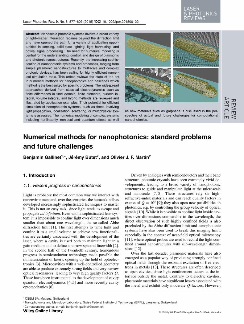
Figure 1 Examples of nanophotonic systems and applications.Red arrows and areas represent light propagation and hot spots,respectively. (a) Coupling and propagation of surface plasmonpolaritons in nanowires. (b) Nanoparticles in the active layer of asolar cell to enhance light localization and harvesting. (c) Scatter-ing and re-emission from a nanoparticle. (d) Nanoantenna withsub-nanometer gap with electron tunneling.
or infinite domain. An algorithm is then used to computethe solution of the approximated problem (for example alinear system of equations). The required computationalmemory and time depend on the problem and the chosenapproach to solve it. Many popular methods have beenextensively reviewed in the framework of computationalelectromagnetics (e.g. Refs. [21,22]), some of them havingbeen quantitatively compared or benchmarked with analyt-ical or experimental results in the field of nanophotonics[23–28]. However, it remains challenging to find practi-cal cases that can fairly benchmark the different numericalmethods. The approach used to generate the approximatedproblem strongly determines the strengths and weaknessesof the numerical method, and as a consequence the kind ofproblems for which it is best suited. In addition, the effi-ciency of a numerical method also includes many differentaspects besides the computation time and memory require-ments: among them, ease of implementation, complexity ofdiscretization, and versatility. Some methods can be usedto calculate a broad range of systems, while others are veryefficient for specific problems. Furthermore, for the userscientist or engineer, a trade-off between the problem tosolve and the method at hand usually has to be found. Forthese reasons, the approach chosen in this review is first toidentify categories of nanophotonic problems which can beseen as fundamental building blocks for modeling nanopho-tonic systems, and then discuss the suitability of numericalmethods to these categories. We distinguish four categoriesof problems: those involving light propagation, light local-ization, light scattering, or multiscale problems. We definethe categories and introduce some potential challenges fortheir numerical modeling. Some examples, possibly involv-ing experiments, are chosen from the literature to motivatethe discussion. Figure 1 represents some particular occur-rences in each category.
This first category of problems involves calculations in aone- or two-dimensional sub-diffraction limited light con-finement. This can include waveguides, nanowires, or ar-rays of nanoparticles which support the propagation of sur-face plasmon polaritons (SPPs) (Fig. 1a) [29]. An exampleof a plasmonic waveguide is shown in Ref. [30]: an SPP iscoupled into a thin silver stripe and its propagation proper-ties are measured with a near-field scanning optical micro-scope. The propagation in waveguides can be enhanced bythe use of specific substrates such as Bragg mirrors or pho-tonic crystals [31]. The coupling elements can include grat-ings or Y-couplers [32]. In such systems, the propagationproperties of light need to be evaluated in view of the futureintegration of components in photonic circuits: in partic-ular, the waveguide modes are studied through their reso-nance frequency, field distribution, and propagation losses[33, 34]. Another important figure of merit is the couplingefficiency between circuit elements. The source can bemodeled as, for example, a point-source emitter or a prop-agating waveguide mode. These waveguides are usuallymodeled in a closed (i.e. spatially limited) or quasi-openenvironment (e.g. to study radiation leakage of guided lightin an infinite environment).
1.2.2. Problems based on light localization
One important property of some nanophotonic systems liesin the three-dimensional confinement of light below thediffraction limit, possibly with resonant effects. An insightinto the near-field distribution and more generally the modaldecomposition is the key enabler for the understanding anddesign of efficient systems such as low-threshold lasers [35]or sensors with a high signal-to-noise ratio [36]. Studies ofthe near field can include the calculation of the differentmodes, including their resonance frequencies and field dis-tribution. An example is shown in Fig. 1b: the hot spotsof the electromagnetic field around the nanoparticles uponsunlight illumination enhance the absorption in an activelayer. Examples include optoelectronic devices such as so-lar cells or photodetectors which can be enhanced by thelocalization of light in the active material [37–39] and ther-mal [40–42] or near-field imaging [30] devices. The studyof spontaneous emission in proximity to a nanostructureinvolves the calculation of the local density of optical statesand the far-field radiation leakage pattern of a dipole emit-ter [35]. Efficient sensors such as gas sensors [43] or bio-logical sensors based on surface-enhanced Raman scatter-ing (SERS), surface-enhanced infrared absorption, fluores-cence, or nanoscale refractive index variations rely on theconfinement of the electromagnetic field in specific regionsof space [36].
1.2.3. Problems based on light scattering or emission
This class of problems involves the interaction between ananostructure and propagating light waves. In scattering
experiments, the optical response of a nanostructure upona given illumination is measured. As the distance betweenthe source, the detector, and the target is usually orders ofmagnitude larger than the characteristic dimensions of thescatterer, the environment can be modeled as an infinitehomogeneous background. Some examples can include ananoparticle embedded in a dielectric material (Fig. 1c),placed on a substrate or on a multilayered medium such asa Bragg reflector. The response of an individual nanopar-ticle is usually characterized by its scattering, absorption,and extinction cross sections [44]. A large category of prob-lems include arrays of nanostructures with various sizes. Inperiodic systems, the observables are the reflection, trans-mission, and absorption coefficients. An example of re-flective surfaces is shown in Ref. [45]: here, plasmonicnanostructures are used to generate structural colors. Theoptical properties of the structured surface are tailored togenerate a variety of colors towards a realistically renderedimage. Structural colors can be also generated from high-refractive-index nanoparticles [46] or nanowires [47]. Inthe design of nanoantennas or metasurfaces, an in-depthdesign of the angular emission pattern, including the fieldphase and intensity, is also necessary [17, 48]. As anotherexample, in Ref. [49] electron energy loss spectroscopy(EELS) measurements are compared to simulations of elec-tron scattering on nanoparticles: this is usually modeled byconsidering a fast-moving dipolar light source.
1.2.4. Multiscale problems
A large quantity of recently developed nanophotonic sys-tems require a modeling approach beyond the linear con-stitutive relations for the electric and magnetic fields oreven Maxwell’s equations themselves. This is the case forexample for magneto-optical systems [50] or nonlinear op-tical effects such as second harmonic generation (SHG)or third harmonic generation (THG) in plasmonic nanos-tructures [51]. In active and optoelectronic devices such aslight-emitting diodes, organic light-emitting diodes, lasers,or solar cells, the electronic behavior needs to be mod-eled together with the optical behavior [35, 38, 39]. Foranother class of systems where the size of the plasmonicstructures is comparable to the mean free path of electrons(e.g. Fig. 1 d showing a dipole nanoantenna with a deepsub-wavelength gap), an in-depth knowledge of the dy-namics of the material is required, with even in some casesfully quantum mechanical calculations [52]. In the case ofnanostructured graphene, the two-dimensional nature of thematerial requires an accurate description of the electronicband structure prior to the study of the plasmonic modes[53]. In nanoparticle-enhanced photochemistry, charge car-riers are excited on the metal surface and used to activatechemical bonds and chemical transformations in an adsor-bate: an understanding of the mechanisms will in generalrequire knowledge of the energy levels and interactions inthe nanoparticle–adsorbate system [54].
580 B. Gallinet et al.: Numerical methods for nanophotonics
1.3. Outline
Four categories of problems are identified in Section 1.2and form together a basis for the modeling of nanopho-tonic systems: problems involving light propagation, lo-calization, scattering, or multiscale problems. This reviewis organized in two main sections. Section 2 is dedicatedto problems which can be numerically modeled by dis-cretizing Maxwell’s equations and the linear constitutiverelations for the electric and magnetic fields. The currentlymost popular methods are reviewed: for each method, themain equations are introduced and latest examples of ap-plications or developments in nanophotonics are provided,with the goal of illustrating their respective strengths andweaknesses. However, it is beyond the scope of this reviewto give a detailed description of the methods or to quantita-tively compare their efficiency, for which well-documentedbooks or review articles are cited in the text. Among themost popular methods, two main categories can be distin-guished: differential and integral methods. Popular differ-ential methods discretize the differential form of Maxwell’sequations in a finite space. They include the finite differ-ences in time domain (FDTD) and the finite element (FE)methods, as well as hybrid methods. Volume or surface inte-gral methods restrict the discretization to the nanostructureand make use of the Green’s dyadic function to computethe solution. Hybrid methods combine advantages of sev-eral methods together, which broadens their field of applica-tions. Some popular methods based on scattering and trans-fer matrices are also discussed. Finally, the advantages andlimits of the different numerical methods are assessed in thiscontext.
Section 3 reviews specific examples of nanophotonicsystems for which numerical simulations require modelsbeyond the classical nature of Maxwell’s equations and thelinear form of the constitutive relations for the electric andmagnetic fields, usually with a more accurate descriptionof the materials at the nanoscale. This comes together withan increased complexity of implementation and requiresthe use of state-of-the-art methods or the development ofnovel tailor-made techniques. In particular, nonlinear op-tical effects, the nonlocal correction to the permittivity ofnanostructures, and the field of quantum plasmonics arediscussed. Finally, the rapidly growing field of modeling ofgraphene plasmonics is reviewed.
1.4. Target audience
This review is aimed at providing engineers and experimen-tal researchers in nanophotonics with a basic knowledge ofthe advantages and limitations of numerical methods. Somefundamental equations of the methods as well as applica-tions or developments in the recent literature are selectedin order to provide the reader with the ability to make aninformed choice of the method that is the most appropriateto the problem at hand.
Researchers in computational nanophotonics will alsofind a review of the latest developments in the field through
selected publications, as well as a discussion of the futurepossible directions in developing new methods or improv-ing the existing ones. The far-reaching goal of this commu-nity is to enable the use of multiscale and highly versatilenumerical methods that are able to efficiently handle arbi-trary large and multiscale systems.
2. Numerical methods based on classicalMaxwell’s equations
In this section, each method is briefly described throughits fundamental equations in order to give an intuitive un-derstanding of the type of problem for which it is bestsuited. The emphasis is put on classical numerical meth-ods that are designed to handle a relatively broad varietyof systems: the so-called differential and integral meth-ods. This description is supported by application exam-ples from the recent literature. At this point, it must bementioned that an exhaustive list of examples illustrat-ing every particular feature of the methods would prac-tically be impossible, given the variety of methods andexisting nanophotonic systems. Here, the examples are se-lected because they either clearly illustrate an advantageor limitation of a given method, or highlight cases wheresimulations could model successfully an experimental re-sult, or bring a new layer of understanding of a particulareffect.
Differential methods solve Maxwell’s equations in theirdifferential form. They rely on a volume discretization ina finite computational domain. A first approach consistsof directly discretizing Maxwell’s equations in time andspace using finite differences: this is the core of the FDTDmethod which is discussed in Section 2.1. On the otherhand, the FE method in Section 2.2 consists of expandingthe electromagnetic fields as local functions in elements,which results in higher accuracy in the frequency domain.Its extension to the time domain is discussed in Section2.3, together with the discontinuous Galerkin time-domain(DGTD) method. Integral methods transform Maxwell’sequations in an integral form through the use of the Greenfunction and discretization is reduced to the nanostructuredobjects. A first approach consists of restricting the dis-cretization of the problem to the volume of the objects.These methods are usually called volume integral equation(VIE) methods and are reviewed in Section 2.4. On the otherhand, for piecewise homogeneous objects, the discretiza-tion can be further reduced to the surface boundaries. Themethods using these approaches are called surface integralequation (SIE) methods and are reviewed in Section 2.5. InSection 2.6, hybrid methods and geometry-specific meth-ods such as the T -matrix method, the rigorous coupledwave analysis (RCWA), or semi-analytical methods are dis-cussed. For further details on the implementation of thesemethods, the reader is referred to the related books or re-view articles. The summary (Section 2.7) takes the form ofa table evaluating the methods and their compatibility withthe different nanophotonic problems identified in Section
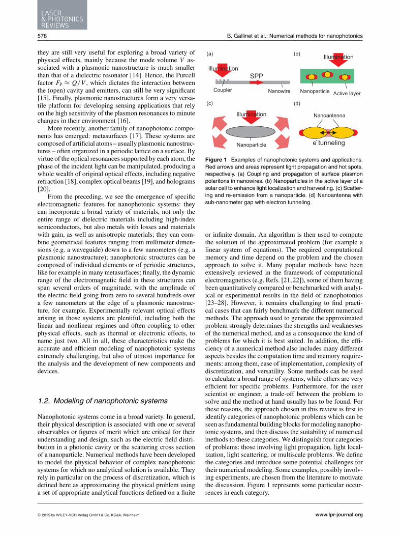
Figure 2 Examples of discretization for computational modeling of an optical nanoantenna. (a) Sketch of the nanostructure sandwichedbetween a substrate (e.g. a quartz wafer) and a superstrate (e.g. air). (b) Finite differences in time domain method, with discretizationin the nanostructure, the substrate, and the superstrate using a Cartesian grid. (c) Finite element or discontinuous Galerkin timedomain method, with discretization of the nanostructure, the substrate, and the superstrate using tetrahedral elements. (d) Discretedipole approximation, with discretization in dipoles inside the nanostructure. (e) Surface integral equation method, with discretizationin triangular elements at the surface of the nanostructure.
1.2: problems based on light propagation, localization andscattering.
2.1. Finite differences in time domain
The FDTD method is one of the most popular methodsin nanophotonics because of its ability to handle a largevariety of problems [55]. In this method, both time andspace are discretized, i.e. all spatial and temporal deriva-tives in Maxwell’s curl equations are replaced by finitedifference quotients[21, 56]. In Fig. 2b, an example of dis-cretization of a metallic nanoantenna on a substrate inthe framework of FDTD is shown. The respective vol-umes of the nanostructure, the substrate, and the super-strate are represented by a staircase approximation. Thepopular algorithm introduced by Yee [57] is briefly shownhere; a more detailed account can be found in, for example,Refs. [21, 55, 56].
In the presence of source currents J and charges ρ,Maxwell’s equations in their differential form are givenby
∇ × H = ∂D∂t
+ J (1)
∇ × E = −∂B∂t
(2)
∇ · D = ρ (3)
∇ · B = 0. (4)
In the Yee algorithm, a Cartesian grid of rectangularcells with side lengths �x , �y, �z for the spatial dis-cretization and a time step �t for the temporal dis-cretization are chosen. Faraday’s law without current isconsidered as an example (Eq. (2)). The same proce-dure can be directly applied to Ampere’s law (Eq. (1))and to the introduction of current sources at specificpoints of the grid. Introducing the notation E(x, y, z, t) =En( j, k, l), where x = j�x , y = k�y, z = l�z, t =n�t , j, k, l, n ∈ N, one obtains the discretization of the
x-component of Eq. (2):
Bn+1/2x
(j + 1
2, k, l
)
= Bn−1/2x
(j + 1
2, k, l
)
− �t
�y
[En
z
(j + 1
2, k + 1
2, l
)
− Enz
(j + 1
2, k − 1
2, l
)]
+ �t
�z
[En
y
(j + 1
2, k, l + 1
2
)
− Eny
(j + 1
2, k, l − 1
2
)]. (5)
Equation (5) implies that the magnetic field at the time in-crement n + 1/2 is updated from the magnetic field at timeincrement n − 1/2 and the electric field at time incrementn in a leapfrog manner. This procedure can be easily gener-alized to the other components of Eq. (2) where the electricfield at time increment n + 1 is updated from the electricfield at time increment n and the magnetic field at timeincrement n + 1/2. This way, the electromagnetic field canbe computed at all time over the computational grid. OnlyAmpere’s and Faraday’s laws are explicitly time-stepped,because the Gauss laws (Eqs. (3) and (4)) are enforcedimplicitly with this FDTD approach.
In general, the permittivity undergoes spatial variationswithin a grid cell: the permittivity in each cell is then cal-culated as an average value, following, for example, theMaxwell–Garnett rule for dielectric materials [21]. The sizeof the discrete cells is critical for achieving a sufficientlyhigh numerical accuracy. It is usually recommended that thespatial increment �x , �y, and �z should not be larger thanλ/20, where λ denotes the wavelength of the incident wave[21]. In order to ensure a stable numerical result, the timeincrement should in addition satisfy the Courant conditiongiven by [56]
582 B. Gallinet et al.: Numerical methods for nanophotonics
It was recently shown that the time increment should beas large as possible, but within the Courant limit [58]. Ascan be seen in Eq. (5), the Yee algorithm uses an orthog-onal uniform grid. It is second-order accurate by natureof the central-difference approximation used to realize thefirst-order spatial and temporal derivatives. However, sucha simple approach can yield numerical inaccuracies of vari-ous kinds: (1) when the space increment is not small enoughto resolve the high field gradients in particular regions ofspace, for example in a resonant cavity; (2) when the po-sition of the cell does not follow the shape of the mate-rial boundaries, resulting in a staircase representation andimplementation for complex geometries. Among the ap-proaches that can enhance the spatial resolution, one cancite the use of a nonhomogeneous grid [59] or the gen-eralization of the Yee algorithm to irregular nonorthogonalunstructured grids [60]. As electromagnetic fields can reachhigh gradients around nanophotonic resonators, great atten-tion must be given to the modeling of such materials foraccurate and reliable results [55]. Another challenge relatedto the FDTD gridding arises from its numerical dispersion.The numerical phase velocity of waves depends on the prop-agation direction, which can be problematic for long-rangepropagation. This source of inaccuracy can be reduced ifa sufficiently fine gridding is chosen, or with the use ofmitigation algorithms [56]. Only the field from the previ-ous time step is needed to compute the new field. Thus,the required computational memory scales only with thevolume of the computational domain, which makes FDTDefficient for large systems. The number of numerical oper-ations in FDTD scales with the fourth power of the particlesize [21, 61].
The implementation of time-domain methods to peri-odic systems has fundamental limitations arising from theperiodic boundary conditions. Valid results can be obtainedat normal incidence (i.e. when there is no phase delay be-tween cells), but oblique incidence requires using the fieldcomponents backwards and forwards in time. Some meth-ods have been introduced to mitigate this fundamental lim-itation, among which are those applying a field transforma-tion to eliminate the time delay across the FDTD grid witha supplementary computational cost [56].
In numerical methods based on the differential formof Maxwell’s equations, boundary conditions are appliedto the fields. They can be of several types: Dirichlet, vonNeumann, or their combination. Also, in systems with dis-crete symmetry, some nontrivial symmetry-driven bound-ary conditions can be enforced on truncated domains [62].For the case of theoretically infinite environments where theSommerfeld radiation condition is applied to the fields (e.g.for scattering or radiation problems), the finite memory al-location means that the computational domain must stillbe finite. The boundary should reproduce as accurately aspossible a homogeneous nonlossy infinite medium, i.e. non-physical reflections must be minimized. Absorbing bound-ary conditions were introduced, but they have the limita-tions of residual reflections depending on the frequency andthe incidence angle [56,63]. In order to solve this problem,the perfectly matched layer (PML) was introduced [64],
which is a layer of lossy material with a perfectly matchedinterface that does not reflect a plane wave for all frequen-cies and all angles of incidence and polarizations. PMLs canbe seen either as coordinate stretching in the frequency do-main [66] or as an artificial anisotropic absorbing medium[67]:
ε = �ε,μ = �μ,� =⎛⎝
sy sz
sx0 0
0 sx szsy
0
0 0 sx sy
sz
⎞⎠, (7)
where the PML parameters s j ( j = x, y, z) are chosen ass j (ω) = 1 − σ j/(iω) and σ j controls the damping of a wavepropagating along the i-direction. Further designs of thePML parameters can be implemented to accelerate the de-cay of propagating or evanescent waves [56, 63]. Specialcare should be taken with the use of PMLs, because numer-ical reflection errors can alter the numerical accuracy. Fur-thermore, the PML approach breaks down when the distri-bution of the permittivity at the edges of the computationaldomain is not homogeneous in the direction perpendicularto the PML, such as a waveguide entering a PML with anangle [68]; in such cases, the use of absorbing boundaryconditions is recommended.
Some materials that can be found in photonic nanos-tructures such as metals or semiconductors are dispersive.In particular, the dispersion of a metallic material deter-mines the plasmon resonance frequency and markedly af-fects the optical properties [69]. In numerical simulations,a frequency-dependent dielectric permittivity is includedto account for this effect, which can be evaluated for in-stance with the Drude model or from experimental data.An example of a frequency-dependent dielectric functionis illustrated in Fig. 3, where a quantum dot nanocrystalof CdSe is placed in the gap of a pair of silver nanopar-ticles. A single Lorentzian peaked at the quantum dot’sresonance frequency is considered for modeling its permit-tivity. The real-valued time-domain susceptibility functionχ (t) is obtained by inverse Fourier transformation. At anypoint in a linearly dispersive medium, the time-dependentelectric flux density is calculated from the electric field in-tensity. This implies in particular that the electric flux takesits value from the history of the system. In time-domainmethods, the implementation of such dispersive materialsis not straightforward. A popular approach is the piecewise-linear recursive convolution method [70]. In order to avoidthe storage of field values at all times, the piecewise-linearrecursive convolution method introduces a time-dependentvector variable (the recursive accumulator). At each timestep, the accumulator and the fields are updated recursivelyfrom the previous time step. Another method consists ofadding an auxiliary differential equation in the time do-main linking the polarization and the electric flux density:an example of application to the multi-term Debye andLorentz models is shown in Ref. [71].
Another challenge concerns the efficient computation ofscattering from long-duration pulses or plane waves. Thetotal field/scattered field technique, popular in FDTD [72],
Figure 3 Simulation of scattering and extinction cross sectionsof a quantum dot–metal nanoparticle hybrid system using FDTD.(a) Geometry of the system with domains used for the simulations.The blue ellipses represent silver nanoparticles and the red circlerepresents a semiconductor nanocrystal. In (b) and (c), solid blacksquares are values of extinction and scattering cross sections(×103 nm2), respectively. The quantum dot linewidth is 10 meV.The solid lines are fits to a phenomenological coupled-oscillatormodel. Solid circles are extinction and scattering spectra for thesame system but without quantum dot absorption, also calculatedby the FDTD method. Adapted from Ref. [248] with permission.Copyright (2010) Optical Society of America.
splits the electromagnetic fields into two contributions, theincident and scattered fields. If the incident field is a planewave, the time iteration is continued until the fields haveconverged to a steady-state solution. As an illustration inFig. 3, a time-windowed plane wave is incident on a struc-ture, where it is absorbed and scattered. The computational
domain includes a region containing the scattering wherethe total field is computed using the FDTD algorithm and aregion where only the scattered field is computed. The planewhere the wave is generated defines the interface betweenthe total-field and scattered-field regions. The absorptionspectrum is obtained by taking the Fourier transform of theflux through a three-dimensional box around the structure inthe total-field region and the scattering spectrum is obtainedby taking the Fourier transform of the flux through a three-dimensional box around the structure in the scattered-fieldregion.
The far field can also be accurately computed fromthe numerically computed near field without the need ofextending the computation grid [56]: with this techniquecalled the near- to far-field transformation, the Green theo-rem is applied on surface currents that are calculated at theboundaries of the computational domain. In order to obtainthe far-field properties of a system, a pulse can be used asan incident field and the Fourier transform of the field canbe calculated, which yields an entire spectrum in a singlecalculation [56]. This approach requires nevertheless con-tinuing the time iteration until the field values have decayedbelow a given threshold value and is limited in accuracy forresonators with high quality factors which decay slowlywith time.
Finally, time-domain methods such as FDTD can covercalculations of light propagation in a natural way. Propa-gation lengths and radiative as well as nonradiative lossescan be assessed in a variety of nanoscale waveguides madefor instance from nanowires [33], arrays of nanoparticles[73], or nanobelts [74]. In Fig. 4, FDTD calculations wereperformed to determine the propagation lengths of SPPs ingold nanowires. The calculations could first reveal that sev-eral modes were supported by the nanowires, as indicatedby the surface charge distribution. A Gaussian beam witha fixed wavelength was normally incident and focused onthe ends of the nanowires. SPP propagation lengths for dif-ferent nanowires and polarizations were determined fromlinear fits to semilog plots of the time-averaged energy flow(Poynting vector) along the nanowire length as a function ofdistance. It is also discussed in this example that the cross-sectional shape of the nanowires and the charge distributionof the modes play an important role in their respective prop-agation lengths. Apart from commercial softwares, Meep[75] is an example of FDTD open source code.
2.2. Finite elements
The FE method is another popular differential methodin nanophotonics, which allows for accurate computa-tion of the electromagnetic field originally in the fre-quency domain. Hybrid and time-domain methods basedon FEs include the finite elements in time-domain method(FETD) and the DGTD method. A detailed account oftheir implementation and various features can be found inRef. [63].
A linear dependence of the magnetic and electric polar-izations is assumed. Eliminating the magnetic field with the
584 B. Gallinet et al.: Numerical methods for nanophotonics
Figure 4 SPP propagation lengths in gold nanowires calculatedwith FDTD for longitudinal and transverse polarized excitations.The propagation lengths were obtained from fitting the decayprofiles. (a) Pentagon cross section. (b) Star cross section. In-sets: scanning electron microscopy images of the chemicallysynthesized nanowires and computed surface charge distribu-tion. Adapted with permission from Ref. [33]. Copyright (2014)American Chemical Society.
aid of the constitutive relations, the vector wave equation isobtained from Maxwell’s equations:
∇ ×(
1
μ∇ × E
)+ ε
∂2E∂t2
+ σe∂E∂t
= −∂J∂t
, (8)
where μ is the magnetic permeability, ε the electric permit-tivity and σe the electrical conductivity. For time-harmonicfields, an exponential time dependence in e−iωt is assumed.Maxwell’s equations with an electric current source J canbe combined to yield the electric field wave equation in thefrequency domain:
∇ ×(
1
μr∇ × E
)− k2
0εrE = ik0 Z0J, (9)
where μr, εr, k0, and Z0 are the relative permeability, rel-ative permittivity, free space wavevector, and impedance,respectively. The solution of the electric field wave equa-tion (Eq. (9)) with current is sought, in combination withthe general boundary conditions:
1
μrn × (∇ × E) + γen × (n × E) = U, (10)
where γe is a known parameter and U a known vector. Thefollowing functional is considered:
F(E) = 1
2
∫V
[1
μr(∇ × E) · (∇ × E) − k2
oεrE · E]
dV
+∫
S
[γe
2(n × E) · (n × E) + E · U
]dS
− ik0 Z0
∫V
E · J dV . (11)
Seeking for the stationary point of the functional with re-spect to the electric field (δF = 0) is equivalent to solvingthe boundary value problem involving Eqs. (9) and (10).Note that a functional for anisotropic media can be derivedin an equivalent way as in Eq. (11).
The domain V on which the problem is defined isthen separated in a set of elements and the electric fieldis expanded in each element on a set of basis functions.Tetrahedral and hexahedral elements are flexible and canmodel accurately material boundaries (Fig. 2c). As a dif-ferential method, the entire computational domain has tobe discretized: this includes in the example of Fig. 2c thenanostructure, the substrate, and the superstrate. Seekingthe stationary point of the function in Eq. (11) can lead tosolutions that do not fully satisfy the divergence conditioncalled spurious solutions (Eqs. (3) and (4)), as well as todifficulties in imposing boundary conditions and treatingfield singularities at edges and corners. Edge elements withvector basis functions N j were introduced to solve theseissues: these basis functions enforce continuity of the fieldsand their curl, and therefore implicitly satisfy Gauss’ laws.The electric field is expanded as
E =N∑
j=1
E j N j (r), (12)
where N is the number of unknowns, corresponding to thenumber of edges, and E j are the unknown coefficients. Us-ing the decomposition of Eq. (12), the variational problemδF = 0 becomes
The system of equations in Eq. (13) can be written in matrixnotation:
M E = b, (16)
where E is the vector of unknown electric field amplitudes,b is related to the source terms, and M is a sparse matrix.The vector wave equation without source can be consid-ered as well, resulting in the eigenvalue equation M E = 0which can be useful when calculating the eigenmodes ofa nanophotonic resonator. For example, the eigenvalue ina dielectric three-dimensional cavity with Dirichlet bound-ary conditions is k2
0. The calculation of eigenvalue prob-lems using FEs can also be applied to open or lossy cavitiesor waveguides. It must also be mentioned that eigenvalueequations are not specific to FEs but can also be found inother methods in the frequency domain. The basis func-tions are polynomial functions of the position. Althoughthe first-order basis functions show good accuracy, a higherorder convergence rate can be achieved using higher ordervector elements [76, 77]. As a differential method, the FEmethod requires the use of PMLs, an artificial separationof incident and scattered fields, as well as near- to far-fieldtransformations which complicate the implementation anduse of the method for scattering problems, as explainedin Section 2.1. However, the dispersion of materials andperiodic boundary conditions can be directly implementedsince the FE method is in the frequency domain. Overall,the number of numerical operations in the FE method scalesapproximately with the seventh power of the particle sizewhen Gaussian elimination is used, and can be brought tothe fourth power with the conjugate gradient method [21].The memory consumption scales approximately with thefifth power of the particle size.
In contrast to FDTD, the use of basis functions en-ables one to account for the geometry of nanostructureswith a high accuracy, which can be crucial when studyingthe effect of nanoscale variations of shapes on the opticalproperties [33,78]. The high accuracy of the computed elec-tromagnetic field allows studying the electromagnetic con-finement in nanostructures and in particular the influenceof geometrical parameters on the near-field distribution.This makes FE-based approaches very well suited for thesimulation of systems based on light localization and theirrelated applications [79]. Dispersive materials can also bedirectly implemented as the FE method is in the frequencydomain. In the frequency domain, the modes as well astheir resonance frequencies, losses, and area can be di-rectly calculated, which are critical in the design of cavitiesfor nanolasers [80,81] (an example is shown in Fig. 5). Anaccurate simulation of the near field is also critical to un-derstand and design nanostructures for optical trapping andsensing [82]. In another example, the near-field informa-tion obtained from FE calculations is used to evaluate thetemperature distribution of plasmonic nanostructures usinga thermal transport equation [42].
Figure 5 Near-field properties of an ultraviolet plasmonicnanolaser device computed with the FE method. (a) Schematicof the device. (b) Absolute electric field (|E|) distribution (left)around the plasmonic device with a wavelength of 370 nm, corre-sponding to the lasing wavelength of GaN nanowires. The electricfield direction is indicated by red arrows. The cross-sectional am-plitude (right) is also shown. (c) Calculated local Purcell factordistribution around the GaN nanowire (left) and cross-sectionalPurcell factor plot (right). Adapted with permission from Ref. [81].Copyright (2014) Nature Publishing Group.
The FE method can be extended to the time domainby seeking for the stationary point of the functionalcorresponding to the vector wave equation (Eq. (8)). Thisleads to a differential equation in the time domain whichcan be solved for example using a finite difference scheme.Different time-stepping schemes can be adopted: the mostaccurate approaches (second order, central difference, andNewark methods), however, require solving a system ofequations at each time step, resulting in general in highercomputational costs than FDTD [63]. If linear, rectangularhexahedral elements are adopted and the spatial integrationsare evaluated using the trapezoidal rule, then the FDTD al-gorithm is recovered [56, 83]. Hybrid methods have beenrecently developed in order to benefit from the advantagesof both FDTD and FE methods. In particular, methods havebeen proposed to improve the efficiency of FETD. Thedual-field domain decomposition method divides the com-putational domain into small sub-domains and couples thefields between the sub-domains by exchanging the surfaceequivalent electric and magnetic currents at the sub-domaininterfaces and computes the electric and magnetic fieldsstep by step in a leapfrog manner [84]. In the same spirit,the element-level decomposition method considers each FEas a sub-domain [85]. Techniques which use a combinationof a Cartesian space lattice with a time-domain FE meshconsisting of tetrahedra and pyramids have also been devel-oped [56,86]. Part of the computational domain which doesnot require fine geometrical rendering is discretized usingFDTD and the update of the fields with time is made explic-itly. A FE mesh is implemented on a reduced domain whereaccurate computation is required. In this sub-domain, thefields are updated implicitly and interfaced with the FDTDgrid.
586 B. Gallinet et al.: Numerical methods for nanophotonics
A popular method is the DGTD method [63]. A detailedreview of the method and its application to nanophotonicsis given by Busch et al. [87]. The DGTD method directlysolves Maxwell’s equations inside each element and con-nects them through a numerical flux. The discretization inthe time domain can be made using the central differencemethod in a similar manner to FDTD. This method allowsthe use of higher order expansion and testing functions,providing great accuracy, while solving equations locallywithin each element. It therefore combines the accuracyof high-order FE methods with a time-domain description,which makes it efficient for large systems [88]. Similarlyto the FDTD and FE methods and as a differential method,the DGTD method also requires the use of tailored PMLsand an artificial separation of incident and scattered field,as briefly explained in Section 2.1 and detailed in Ref. [89].Several examples of applications for nanophotonics canbe found, including nanostructured metallic films [89] andsplit-ring resonators [87].
Overall, the methods outlined in this section featurethe typical limitations (such as the challenging implemen-tation of periodic boundary conditions, dispersive materi-als, open boundary conditions, scattering by long-durationfields) and advantages (efficient simulation of large sys-tems, calculation of explicit time-domain decays of waves)of time-domain methods. Great care has also to be takenin order to model highly resonant systems which decayslowly in time. Their advantage as compared to FDTD istheir higher accuracy, which comes at the price of a morechallenging implementation and generally higher compu-tational cost.
2.4. Volume integral methods
VIE methods transform Maxwell’s equations in an inte-gral form to solve for the electromagnetic field on a re-duced volume. There are different approaches for deriv-ing the numerical equations associated with the solution ofMaxwell’s equations in their integral form. Here we willfollow Ref. [90], starting from the vectorial wave equationand draw at the end of the section similarities with themost popular implementation of this approach, the discretedipole approximation (DDA) [91].
Assuming nonmagnetic materials, we consider a scat-terer with permittivity ε(r) embedded in an infinite ho-mogeneous background with permittivity εb. The scattererdoes not need to be homogeneous, but can be composed ofdifferent materials, including metals with a complex per-mittivity; furthermore, it can also be made of anisotropicmaterials [92], although we consider here a scalar permit-tivity for simplicity. Since this approach is in the frequencydomain, all calculations are performed at a single frequencyω and harmonic fields with exp(−iωt) are assumed. Thevolume integral methods presented here consider only theelectric field, since it is in principle sufficient to solve anyelectromagnetic problem with nonmagnetic materials, as isthe case for most nanophotonic systems. This representsan important difference from many other numerical meth-
ods, which usually solve simultaneously for the electricand magnetic fields. In principle, once the electric field isknown for a given problem, the magnetic field can be foundusing Eq. (2); however, this task is not trivial with a finitedifferences approach, since the discretized form of Eq. (2)requires knowing the electric field on several points aroundthe location where the magnetic field is calculated, whichgenerates quite some computational overhead.
When this system is illuminated with an incident fieldE0(r) propagating in the background medium, the total elec-tric field (incident field plus scattered field) is a solution ofthe vectorial wave equation obtained from Eq. (9) in theabsence of currents:
∇ × ∇ × E(r) − k20ε(r) E(r) = 0, (17)
where k20 = ω2/c2 is the vacuum wave number. The key
step in the derivation of the VIE is to consider the scatteringproblem as the superposition of a problem composed of theinfinite homogeneous background εb plus another problem,where the dielectric contrast,
�ε(r) = ε(r) − εb, (18)
describes how the scatterer differs from that background[90]. In this way, the total electric field becomes a solutionof the integral equation
E(r) = E0(r) +∫
Vdr′Gb(r, r′) · k2
0�ε(r′)E(r′), (19)
where the integration runs over the entire scatterer volumeV and Gb(r, r′) is the Green tensor associated with the back-ground. This dyadic has a very simple interpretation. It isa 3 × 3 matrix, the columns of which represent the electricfield at position r for three orthogonal dipoles located atposition r′: the first column corresponds to the three elec-tric field components (Ex , Ey, Ez) for the field radiated bya dipole oriented in the x-direction (Fig. 6a); the secondcolumn gives the three electric field components radiatedby a dipole oriented in the y-direction; and the third columnis the field radiated by a dipole oriented in the z-direction.Consequently, in that formalism, the system is discretizedby assigning to each mesh three orthogonal dipolar polar-izabilities and the corresponding meshes are often repre-sented by spheres (Fig. 2d). This approach is validated bythe fact that the polarizability of a scatterer much smallerthan the wavelength is essentially dipolar [93].
This physical interpretation of the Green tensor as thefield produced by a dipolar source points to an intrinsicdifficulty associated with this method: when the observationpoint r gets closer to the source point r′, the field diverges(the electric field of a dipole diverges at the position of thedipole). Consequently, one must take the principal valuefor the integral in Eq. (19), which leads to the followingdiscretized equation:
Figure 6 (a) The Green tensor used in the VIE represents thefield radiated by a dipole. In free space, only direct radiation ex-ists (dashed line), while (b) in a stratified medium, reflections atthe different interfaces also exist. (c) Light scattering by scatter-ers in a stratified background can easily be computed using thisapproach. In the example, a light-coupling mask used for nano-lithography is decomposed into a stratified background plus a fewscatterers. (d) Intensity distribution in the photoresist for such alight-coupling mask. (e) When an additional anti-reflection layeris used above the substrate, the standing wave in the photoresistdisappears. Adapted from Ref. [99] with permission. Copyright(2001) Optical Society of America.
where the discretized field Ei = E(ri ), the discretized di-electric contrast �εi = �ε(ri ), and the discretized Greentensor Gb
i, j= Gb(ri , r j ) have been introduced for the
N meshes corresponding to the discretized scatterer.This discretization assumes that all these parameters areconstant over one single mesh volume V j . More re-fined discretization approaches have been proposed forEq. (19), using concepts derived from signal processing[94, 95] or from the FE technique [96], although the lat-ter case has only been implemented for two-dimensionalgeometries.
Since this approach relies on the discretization of thescatterer into small volumes, inhomogeneous scatterers caneasily be handled and discretized into a collection of mesheswith different permittivities. The accuracy of the methoddepends on the mesh size used for the discretization; a suffi-cient accuracy for most physical situations is achieved with5 to 10 meshes per wavelength, although the convergenceof the method is not always monotonic [97]. Overall, thenumber of numerical operations scales approximately withthe ninth power of the particle size when Gaussian elimi-
nation is used, and can be brought to the sixth power withthe conjugate gradient method [21] or even further downwith the use of fast Fourier transform techniques [61]. Thememory consumption scales approximately with the sixthpower of the particle size. As a matter of fact, a limitationof this approach lies in the fact that the resulting matrixis dense, non-Hermitian, and can have a large conditionnumber [98].
The simple interpretation of the Green tensor as the fieldof a collection of orthogonal dipoles illustrated in Fig. 6aprompts a very interesting extension of VIEs for light scat-tering in complex backgrounds, especially stratified media.For an infinite homogeneous space, the field radiated by adipole corresponds to direct radiation from the source (atposition r′) to the field point (at position r), as indicated bythe straight radiation line in Fig. 6a. For a stratified back-ground, e.g. composed of three different materials withpermittivities εb1, εb2, and εb3, in addition to this direct ra-diation, additional radiation paths exist with reflection atthe different interfaces (Fig. 6b). These additional paths ac-count for the entire interaction between the scatterer and itssurroundings; hence, by using the Green tensor associatedwith such a stratified medium, i.e. the field generated bya dipole in a layered background, one can compute lightscattering by a scatterer embedded into that backgroundby merely discretizing the scatterer only [99]. For a ho-mogeneous medium, the Green tensor Gb
i, jis analytical;
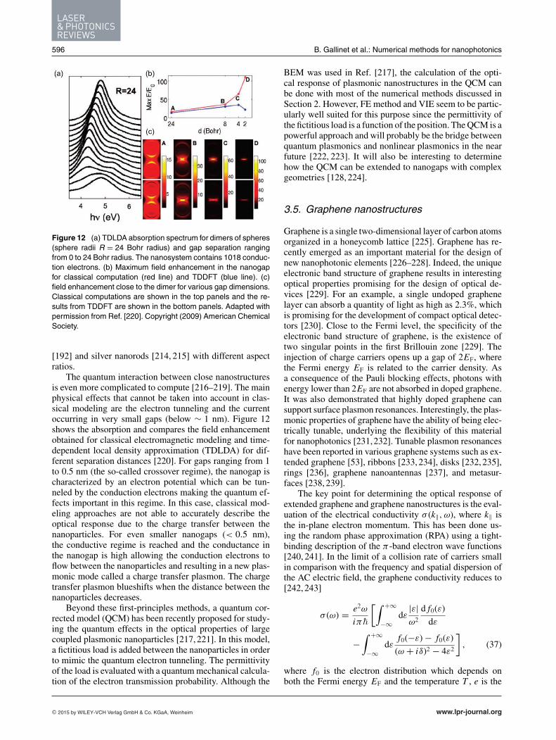
this is no longer the case in a stratified background, wherethe Green tensor must be computed numerically – usuallyin the spectral domain using numerical integration in thecomplex plane – which has an additional, non-negligible,computational cost [100]. This approach is especially ef-ficient when the scatterer volume is limited, compared tothe volume of the stratified background, as illustrated inFig. 6c–e. This figure shows the field distribution producedby a light-coupling mask for nanolithography [101]: themask is made of a soft polymer and includes a thin goldlayer to increase the contrast. It is applied onto the photore-sist, where it produces a strongly localized field distribu-tion, which can be used to expose sub-wavelength features[102]. The geometry is easily decomposed into a stratifiedbackground made of the different homogeneous layers, anda few localized scatterers (Fig. 6c). The numerical solutionof Eq. (20) requires only the discretization of these fewscatterers that link the polymer layer with the photoresist.Note that for some backgrounds, the dielectric contrast cantake arbitrary values, including negative values; this is forexample the case when one simulates light scattering by airbubbles within a dielectric background, leading to �ε < 0.The role played by the background in that type of simulationis illustrated in Fig. 6d and e, which show two simulationswith exactly the same scatterers accounting for the light-coupling mask, but a different background. In Fig. 6e, anadditional layer is introduced in the background (i.e. inthe Green tensor), serving as anti-reflection layer (bottomanti-reflection coating), as is often the case in lithography.Consequently, the standing wave in the photoresist causedby the reflections at the substrate interface (Fig. 6d) is
588 B. Gallinet et al.: Numerical methods for nanophotonics
completely suppressed (Fig. 6e). The numerical effort forboth calculations is almost identical, although the physicalsystems are quite different.
In Eq. (20), the tensors M and L are used to handle thesingularity of the Green tensor [90]. In particular, the tensorL represents the depolarization of the discretized volume[103]. There exists a completely different approach to thediscretization of Eq. (19), where the singular terms M andL are skipped and another value is used for the dielectriccontrast. As a matter of fact, �ε(r) is similar to the di-electric susceptibility χ (r), which in turn can be associatedwith the polarizability α(r) of the scatterer [104]. In theso-called DDA, also sometimes called the coupled dipoleapproximation, the polarizability of the scatterer is used inEq. (20) instead of �ε(r) and the singular terms are omitted[91,105]. To obtain accurate results, the discretization takesinto account the fact that the scatterer is decomposed intoa lattice of dipoles and the polarizatbility of each mesh isobtained from the lattice dispersion relation instead of thescatterer’s material properties [106].
The DDA usually considers a homogeneous back-ground, where the Green tensor has the following additionalsymmetry property: Gb(r, r′) = Gb(r − r′). This transla-tion property is easily understood with Fig. 6a: the fieldradiated at position r by a dipole located at position r′ onlydepends on the relative distance r − r′ between both points;note that this property does not hold in the case of a stratifiedbackground, where the distances between these points andthe interfaces also play a role (Fig. 6b). For a homogeneousbackground, Eq. (19) can be rewritten as
E(r) = E0(r) +∫
Vdr′Gb(r − r′) · k2
0�ε(r′)E(r′), (21)
which represents a convolution between the Green tensorand the source. Such a convolution can be easily computedin Fourier space, especially when the scatterer is discretizedover a regular mesh and fast Fourier transform algorithmscan be used [107]. This has led to an extremely efficient im-plementation of the DDA that uses fast Fourier transformsto speed up the integration [108]. A definite appeal of theDDA is that a very solid implementation of the techniqueis freely available [109].
The VIE method and DDA can be extended to periodicsystems [110–112]. In this case, the periodic boundary con-ditions are handled by a specific Green function for whichefficient acceleration techniques have been developed forits computation [113]. Let us finally mention that Eq. (19)forms the basis for a very general approximation for lightscattering, namely the Born approximation. This approxi-mation consists of using the illumination field E0(r) insteadof the unknown field E(r′), thus transforming the implicitEq. (19) into an explicit equation, with the unknown electricfield only on the left-hand side [114]. The procedure canbe iterated, using the result of this first step as illuminationfield in Eq. (19) and so on. From a physical point of view,the first term in this Born series corresponds to the responseof the different meshes in the system to the excitation, thesecond term to the first interaction between the meshes,
and so on. In principle, this procedure should converge tothe self-consistent solution of Eq. (19); unfortunately, theconvergence is rather poor, especially for highly scatter-ing materials, as encountered in nanophotonics [115]. ThisBorn series has, however, inspired an iterative algorithm forthe solution of Eq. (19) [116].
2.5. Surface integral methods
Surface integral methods reduce the computation of anelectromagnetic scattering problem with open boundaryconditions to the surface boundaries of materials. Theywork therefore best for piecewise homogeneous media. Twomethods are used extensively in nanophotonics, namely theSIE method [26,117,118] and the boundary element method(BEM) [119]. We discuss first the SIE method, followed bythe BEM and distinguish them by their usual implementa-tion in nanophotonics.
The computational space is divided into domains Vn ofrelative permittivity εn and relative permeability μn . FromEq. (9), the electric field E in each region must satisfy theequation
∇ × ∇ × E(r) − k2nE(r) = iωμnj(r), r ∈ Vn, (22)
where k2n = ω2εnμn is the wavenumber for electromag-
netic waves in region Vn and j denotes the volume cur-rent density. A dyadic Green function G
nfor region Vn is
introduced:
∇ × ∇ × Gn(r, r′) − k2
n Gn(r, r′) = 1δ(r − r′). (23)
The equivalent surface current densities Jn = nn × H andMn = −nn × E defined on the boundaries ∂Vn of the do-mains are introduced. Using Green’s theorem, the electricfield integral equation (EFIE) and the magnetic field integralequation (MFIE) can be derived on the domain boundaries[117]. A technique for solving the EFIE and the MFIE is themethod of moments (MoM) [120]. The equivalent surfacecurrents can be expanded in terms of Rao–Wilton–Glisson(RWG) basis functions fn
i building a triangular mesh ap-proximating the boundary surface ∂Vn [121]:
Jn =∑
i
αi fni (24)
Mn =∑
i
βi fni , (25)
where the index i labels the different edges within all re-gions (Fig. 2e). If two RWG functions fn
i and fn′i are asso-
ciated with the same edge, the conservation of current on∂Vn = ∂Vn′ between the two adjacent regions Vn and Vn′
implies fni = −fn′
i . If more than two regions are touchingan edge, all the expansion coefficients related to this edgeare identified. In this case, more than one RWG function isassociated with the same edge, but only one per adjacentregion. If the region Vn is not adjacent to the edge i , then
fni ≡ 0. The Galerkin method is applied, multiplying the
EFIE and the MFIE with the basis functions and integrat-ing over ∂Vn . Defining the sets {α} and {β} of expansioncoefficients αi and βi , the EFIE can be written as a matrixequation for {α} and {β} for all regions:
[∑n iωμnDn
∑n Kn
] ·[{α}{β}
]=
∑n
q(E),n, (26)
with sub-matrices
Dni j =
∫∂Vn
dS fni (r) ·
∫∂Vn
dS′ Gn(r, r′) · fn
j (r′), (27)
K ni j =
∫∂Vn
dS fni (r) ·
∫∂Vn
dS′[∇′ × G
n(r, r′)
]· fn
j (r′), (28)
and
q (E),ni =
∫∂Vn
dS fni (r) · Einc
n (r). (29)
In some cases, solving for {α} and {β} with the EFIEor the MFIE does not result in the same values and canlead to large errors. Several combinations of SIEs can beconsidered, with different accuracy and convergence prop-erties [122, 123]. The Poggio–Miller–Chang–Harrington–Wu–Tsai (PMCHWT) formulation combines EFIE andMFIE to solve them simultaneously [124]. Although thePMCHWT formulation might lead to poor conditioningof the system matrix and a slow convergence of iterativesolvers [125], it has proven to give stable and accurate re-sults [126, 127], even in resonant conditions [117]. In thatcase, the EFIE and the MFIE are combined:
[∑n iωμnDn
∑n Kn∑
n Kn −∑n iωεnDn
]·[{α}{β}
]
=∑
n
[q(E),n
q(H ),n
], (30)
with
q (H ),ni = −
∫∂Vn
dS fni (r) · Hinc
n (r). (31)
There are several ways to solve Eq. (30), among which areGaussian elimination, LU factorization, and iterative meth-ods. Overall, the number of numerical operations scales ap-proximately with the sixth power of the particle size whenGaussian elimination is used, and can be brought to thefourth power with the conjugate gradient method [21]. Thememory consumption scales approximately with the sixthpower of the particle size. Once Eq. (30) has been solvedon the domain boundaries, the electric and magnetic fieldscan be directly calculated at all points in space.
As a frequency-domain method, the SIE method candirectly handle dispersive materials (similarly to the FEand VIE methods discussed previously). The matrix ele-ments of Eq. (27) can be turned into integrals involvingthe scalar Green function Gn(r, r′) or its gradient in theirintegrand, which is known to be divergent for |r′ − r| → 0.This behavior of the Green function can also lead to in-accurate results in the numerical evaluation of the matrixelements relative to neighboring triangles. An elegant wayto overcome this difficulty is to separate the Green func-tion into a singular part that can be integrated in a closedform and a smooth, slowly varying part that can be ac-curately integrated numerically. Highly conductive metalswith Green function approaching a Dirac distribution cantherefore be handled accurately. The same procedure can berepeated when evaluating the electric and magnetic fields,which guarantees an accurate field evaluation close to thescatterer surface. Similarly to the VIE method and as op-posed to differential methods, the scattering, absorption,and extinction cross sections can be directly obtained with-out the use of absorbing boundary conditions. The dis-cretization in elements allows for a great flexibility in ren-dering complex shapes, such as the defects that can arisein nanofabrication and their effect on optical properties.The SIE method was used in particular to investigate thenear field and far field of realistic nanoantennas and com-pared them to that of idealized geometries [128]. Althoughtheir far field is comparable, the location of hot spots ofthe electromagnetic near field in the respective structuresmarkedly varies, following the local variations of the shape.This has a strong influence on SERS or fluorescence signals[128, 129].
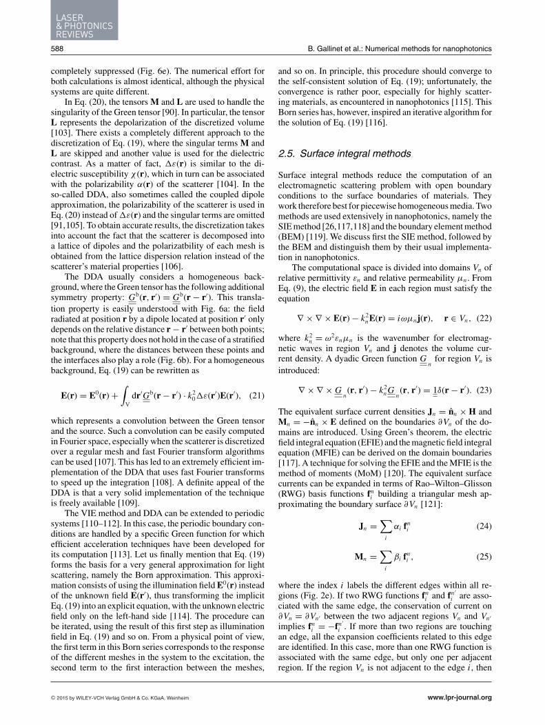
The SIE method can be generalized to multilayeredplasmonic systems [130]. The Green function of homo-geneous media (Eq. (23)) is replaced by the Green func-tion of a layered medium Green function. Although thecomputation of this specific Green function is intensive,the discretization and the resulting system of equationsare reduced to the nanostructured scatterers only. Com-pared to the VIE method, additional complications arisein the implementation due to the need to compute thecurl of the Green function. In Ref. [130], this approachis used to study the spontaneous emission in complex mul-tilayered plasmonic systems. Similarly to the VIE method,the SIE method can be generalized to periodic structures[113,131,132]. Reflection, transmission, and absorption areexamples of measurable quantities that can be delivered, inaddition to phase information of the field as well as ordersof diffraction. An example of implementation to a com-plex resonator supporting Fano-like plasmonic resonancesis shown in Fig. 7. The ability to monitor simultaneouslythe near field and the far field of the SIE method has re-vealed their relation [133, 134]. In particular, it has beenobserved that the maximum in field enhancement does notcorrespond to particular features of the far field (neithera local maximum nor minimum) but is determined by thecondition of Fano interference. Quantitative information onthe field enhancement is also obtained with the SIE method:in this case, the intensity of the near field at the resonance
590 B. Gallinet et al.: Numerical methods for nanophotonics
-100 -50 0 50 100-100
-50
0
50
100
x [nm]
z [n
m]
1. 1.5 2. 2.50.
0.25
0.5
0.75
1.
Energy [eV]
Ref
lect
ance
1. 1.5 2. 2.50.
50.
100.
150.
Energy [eV]
Max
.Int
.Enh
ance
men
t
(a) (b) (c)
Figure 7 Fano resonance in a periodic system of strongly cou-pled gold nanowires. (a) Reflectance spectrum for top illumina-tion. (b) Maximum intensity enhancement sampled at a distanceof 1 nm around the surface. (c) Normalized electric field inten-sity enhancement with field lines. Adapted from Ref. [133] withpermission. Copyright (2011) Optical Society of America.
wavelength increases to 200 times the intensity of the inci-dent field.
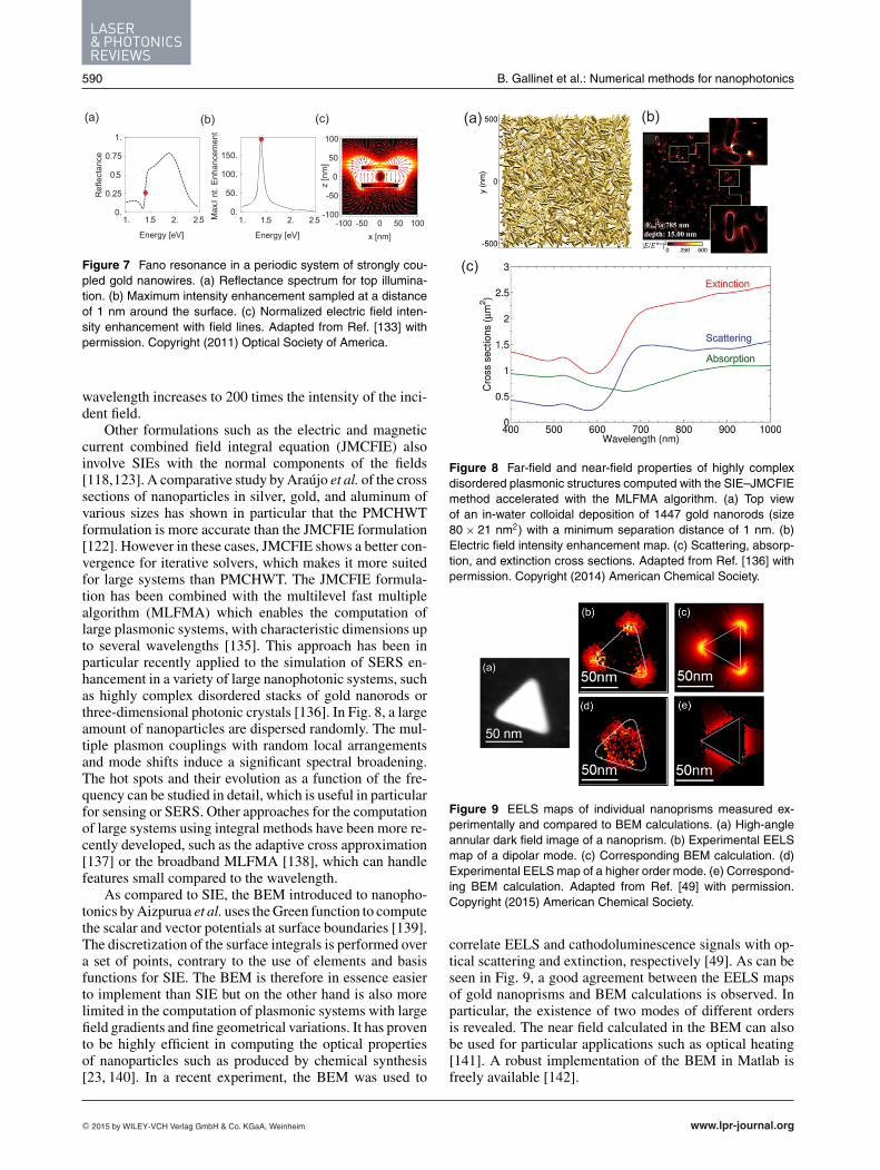
Other formulations such as the electric and magneticcurrent combined field integral equation (JMCFIE) alsoinvolve SIEs with the normal components of the fields[118,123]. A comparative study by Araujo et al. of the crosssections of nanoparticles in silver, gold, and aluminum ofvarious sizes has shown in particular that the PMCHWTformulation is more accurate than the JMCFIE formulation[122]. However in these cases, JMCFIE shows a better con-vergence for iterative solvers, which makes it more suitedfor large systems than PMCHWT. The JMCFIE formula-tion has been combined with the multilevel fast multiplealgorithm (MLFMA) which enables the computation oflarge plasmonic systems, with characteristic dimensions upto several wavelengths [135]. This approach has been inparticular recently applied to the simulation of SERS en-hancement in a variety of large nanophotonic systems, suchas highly complex disordered stacks of gold nanorods orthree-dimensional photonic crystals [136]. In Fig. 8, a largeamount of nanoparticles are dispersed randomly. The mul-tiple plasmon couplings with random local arrangementsand mode shifts induce a significant spectral broadening.The hot spots and their evolution as a function of the fre-quency can be studied in detail, which is useful in particularfor sensing or SERS. Other approaches for the computationof large systems using integral methods have been more re-cently developed, such as the adaptive cross approximation[137] or the broadband MLFMA [138], which can handlefeatures small compared to the wavelength.
As compared to SIE, the BEM introduced to nanopho-tonics by Aizpurua et al. uses the Green function to computethe scalar and vector potentials at surface boundaries [139].The discretization of the surface integrals is performed overa set of points, contrary to the use of elements and basisfunctions for SIE. The BEM is therefore in essence easierto implement than SIE but on the other hand is also morelimited in the computation of plasmonic systems with largefield gradients and fine geometrical variations. It has provento be highly efficient in computing the optical propertiesof nanoparticles such as produced by chemical synthesis[23, 140]. In a recent experiment, the BEM was used to
Figure 8 Far-field and near-field properties of highly complexdisordered plasmonic structures computed with the SIE–JMCFIEmethod accelerated with the MLFMA algorithm. (a) Top viewof an in-water colloidal deposition of 1447 gold nanorods (size80 × 21 nm2) with a minimum separation distance of 1 nm. (b)Electric field intensity enhancement map. (c) Scattering, absorp-tion, and extinction cross sections. Adapted from Ref. [136] withpermission. Copyright (2014) American Chemical Society.
Figure 9 EELS maps of individual nanoprisms measured ex-perimentally and compared to BEM calculations. (a) High-angleannular dark field image of a nanoprism. (b) Experimental EELSmap of a dipolar mode. (c) Corresponding BEM calculation. (d)Experimental EELS map of a higher order mode. (e) Correspond-ing BEM calculation. Adapted from Ref. [49] with permission.Copyright (2015) American Chemical Society.
correlate EELS and cathodoluminescence signals with op-tical scattering and extinction, respectively [49]. As can beseen in Fig. 9, a good agreement between the EELS mapsof gold nanoprisms and BEM calculations is observed. Inparticular, the existence of two modes of different ordersis revealed. The near field calculated in the BEM can alsobe used for particular applications such as optical heating[141]. A robust implementation of the BEM in Matlab isfreely available [142].
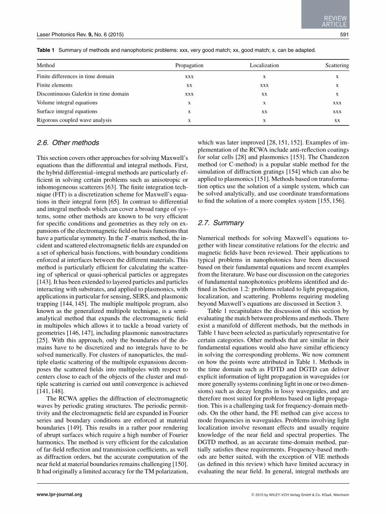
Table 1 Summary of methods and nanophotonic problems: xxx, very good match; xx, good match; x, can be adapted.
Method Propagation Localization Scattering
Finite differences in time domain xxx x x
Finite elements xx xxx x
Discontinuous Galerkin in time domain xxx xx x
Volume integral equations x x xxx
Surface integral equations x xx xxx
Rigorous coupled wave analysis x x xx
2.6. Other methods
This section covers other approaches for solving Maxwell’sequations than the differential and integral methods. First,the hybrid differential–integral methods are particularly ef-ficient in solving certain problems such as anisotropic orinhomogeneous scatterers [63]. The finite integration tech-nique (FIT) is a discretization scheme for Maxwell’s equa-tions in their integral form [65]. In contrast to differentialand integral methods which can cover a broad range of sys-tems, some other methods are known to be very efficientfor specific conditions and geometries as they rely on ex-pansions of the electromagnetic field on basis functions thathave a particular symmetry. In the T -matrix method, the in-cident and scattered electromagnetic fields are expanded ona set of spherical basis functions, with boundary conditionsenforced at interfaces between the different materials. Thismethod is particularly efficient for calculating the scatter-ing of spherical or quasi-spherical particles or aggregates[143]. It has been extended to layered particles and particlesinteracting with substrates, and applied to plasmonics, withapplications in particular for sensing, SERS, and plasmonictrapping [144, 145]. The multiple multipole program, alsoknown as the generalized multipole technique, is a semi-analytical method that expands the electromagnetic fieldin multipoles which allows it to tackle a broad variety ofgeometries [146, 147], including plasmonic nanostructures[25]. With this approach, only the boundaries of the do-mains have to be discretized and no integrals have to besolved numerically. For clusters of nanoparticles, the mul-tiple elastic scattering of the multipole expansions decom-poses the scattered fields into multipoles with respect tocenters close to each of the objects of the cluster and mul-tiple scattering is carried out until convergence is achieved[141, 148].
The RCWA applies the diffraction of electromagneticwaves by periodic grating structures. The periodic permit-tivity and the electromagnetic field are expanded in Fourierseries and boundary conditions are enforced at materialboundaries [149]. This results in a rather poor renderingof abrupt surfaces which require a high number of Fourierharmonics. The method is very efficient for the calculationof far-field reflection and transmission coefficients, as wellas diffraction orders, but the accurate computation of thenear field at material boundaries remains challenging [150].It had originally a limited accuracy for the TM polarization,
which was later improved [28, 151, 152]. Examples of im-plementation of the RCWA include anti-reflection coatingsfor solar cells [28] and plasmonics [153]. The Chandezonmethod (or C-method) is a popular stable method for thesimulation of diffraction gratings [154] which can also beapplied to plasmonics [151]. Methods based on transforma-tion optics use the solution of a simple system, which canbe solved analytically, and use coordinate transformationsto find the solution of a more complex system [155, 156].
2.7. Summary
Numerical methods for solving Maxwell’s equations to-gether with linear constitutive relations for the electric andmagnetic fields have been reviewed. Their applications totypical problems in nanophotonics have been discussedbased on their fundamental equations and recent examplesfrom the literature. We base our discussion on the categoriesof fundamental nanophotonics problems identified and de-fined in Section 1.2: problems related to light propagation,localization, and scattering. Problems requiring modelingbeyond Maxwell’s equations are discussed in Section 3.
Table 1 recapitulates the discussion of this section byevaluating the match between problems and methods. Thereexist a manifold of different methods, but the methods inTable 1 have been selected as particularly representative forcertain categories. Other methods that are similar in theirfundamental equations would also have similar efficiencyin solving the corresponding problems. We now commenton how the points were attributed in Table 1. Methods inthe time domain such as FDTD and DGTD can deliverexplicit information of light propagation in waveguides (ormore generally systems confining light in one or two dimen-sions) such as decay lengths in lossy waveguides, and aretherefore most suited for problems based on light propaga-tion. This is a challenging task for frequency-domain meth-ods. On the other hand, the FE method can give access tomode frequencies in waveguides. Problems involving lightlocalization involve resonant effects and usually requireknowledge of the near field and spectral properties. TheDGTD method, as an accurate time-domain method, par-tially satisfies these requirements. Frequency-based meth-ods are better suited, with the exception of VIE methods(as defined in this review) which have limited accuracy inevaluating the near field. In general, integral methods are
592 B. Gallinet et al.: Numerical methods for nanophotonics
also limited to smaller systems as the FE method. For lightscattering, integral methods are the preferred choice. SIEcan handle larger systems than VIE but is also limited topiecewise homogeneous scatterers. RCWA has in compari-son less flexibility in geometries, although it is particularlyefficient for periodic systems.
In general, it has been shown that there always exists oneor several methods that are particularly suited for a givencategory of problems. In these cases, the structure of thefundamental equations of the methods shows that they areable to directly and efficiently provide a solution. In mostcases when the match between the method and the systemsis not optimal, the method can still provide a solution butan additional development or computational effort may berequired. The modeling of nanophotonic systems shouldinvolve finding the solution of one or several problems in-cluded in these categories. The reader is invited to considerthe ranking of the associated columns in order to make achoice of method: for example, in the case of a quantum dotwith a nanoantenna (such as in Ref. [48]), the coupling fromthe quantum dot to the near field as well as the radiationpattern of the nanoantenna are important for the emissionefficiency. In such cases, the input from the localization andscattering columns should be considered together and SIEmethods appear to be the most efficient. In another example,if the quantum dot is coupled to a waveguide, the FE andDGTD methods are the most appropriate by consideringinputs from the propagation and localization columns.
3. Next modeling challenges innanophotonics
In this section, we review the different numerical techniquesfor nonlinear and quantum nanophotonics and the upcom-ing challenges related to these recent topics. Nonlinear andquantum effects play an important part in the developmentof modern optics in general and in nanophotonics in par-ticular. Furthermore, a multitude of nonlinear optical pro-cesses can be observed in nanostructures. The aim of thepresent section is not to provide a complete overview ofnonlinear optical processes, but to present some of theirparticularities in relation to suitable numerical treatments(Section 3.1). In Section 3.2, active systems requiring op-tical and electronic simulations are discussed. The recentadvances in nanofabrication have revealed that the predic-tions from classical electromagnetism fail for tiny nanos-tructures and narrow gaps, and the development of new nu-merical approaches including nonlocal dielectric functions(Section 3.3) or quantum effects (Section 3.4) is mandatoryin order to provide accurate evaluation of their optical prop-erties. Finally, the specific and important case of graphenenanostructures is addressed (Section 3.5).
3.1. Nonlinear optical processes
The observation of nonlinear optical processes requireshigh pump intensity. Interestingly, the localization of lightin nanovolume increases the local field intensity making
Figure 10 (a) Jablonski diagrams describing TPPL, SHG, andTHG. Near-field distributions of the second harmonic intensityand the corresponding nonlinear emission patterns computed for(b) an idealized nanoantenna with rectangular arms and (c) arealistic nanoantenna described by a mesh adapted from a scan-ning electron microscope image. Adapted with permission fromRef. [176]. Copyright (2013) American Chemical Society.
the observation of nonlinear optical processes possible atthe nanoscale [51]. Various nonlinear optical processes areobservable in nanophotonics depending on the matter prop-erties and the excitation conditions (Fig. 10a) [51]. Obvi-ously, it is important to classify them in order to developsystematic approaches for their numerical evaluations. Thefirst necessary distinction is between parametric and non-parametric optical processes. Boyd writes is his textbookabout nonlinear optics [157]: “The origin of this terminol-ogy is obscure but the word parametric has come to denotea process in which the initial and final quantum-mechanicalstates of the system are identical.” And “A difference is thatphoton energy is always conserved in a parametric process;photon energy need not be conserved in a nonparamet-ric process, because energy can be transferred to or fromthe material medium.” In other words, there is no transferof energy, momentum, or angular momentum between thenonlinear medium and the electromagnetic wave during aparametric optical process.
Before discussing the parametric processes in greaterdetail, it is worth saying a few words about an impor-tant nonparametric nonlinear optical process, namely two-photon photoluminescence (TPPL), mainly because thisprocess has been widely studied and observed in goldnanostructures [158–160]. TPPL is a three-step processinvolving the excitation of an electron–hole pair by the
absorption of two incident photons, the relaxation of theexcited electrons and holes, and the emission of light due tothe recombination of electron with hole. TPPL results in abroadband signal. The TPPL intensity for an emission fre-quency ω2 resulting from a pumping beam with a frequencyω1 is given by[161]
I (ω2) = η(ω2)|E0|4|L4(ω1)L2(ω2)|, (32)
where ω1 and ω2 are the incident light and TPPL frequen-cies, respectively, and η is a factor related to the intrinsicluminescence spectrum of the material. The local field fac-tors L(ω) at the excitation and emission frequencies arerelated to the electric field enhancement close to the con-sidered nanostructure [161]. More specifically, the localfield factors are defined as the ratio between the local elec-tric field and the incident electric field. The computationof the electric field enhancement can be performed usingone of the numerical methods discussed in this review. Theevaluation of the parameter η is more complicated and re-quires considering the band structure of the studied material[158]. However, this evaluation is not mandatory for under-standing the trend of the influence of plasmon resonance onTPPL and for designing efficient plasmonic nanostructureswith high TPPL for specific applications [162].
Let us now turn our attention to parametric processes.Such nonlinear effects are described by re-writing the po-larization as [157]
The quantities χ (2) and χ (3) are the second- and third-order nonlinear susceptibilities, describing, respectively,the second- and third-order nonlinear optical processes.The second- and third-order nonlinear susceptibilities areresponsible for different nonlinear optical processes. Forexample, the second-order nonlinear susceptibility is re-sponsible for SHG, the process whereby two photons at thefundamental frequency are converted into one at the sec-ond harmonic (SH) frequency. The third-order nonlinearsusceptibility is responsible for THG, the process therebythree photons at the fundamental frequency are convertedinto one at the third harmonic (TH) frequency [157]. Theproperties of nonlinear susceptibilities are directly relatedto the properties of the nonlinear medium and closely re-lated to the symmetry selection rules. For example, it iswell known that SHG (a second-order nonlinear opticalprocess) is forbidden in centrosymmetric media in theelectric dipole approximation, which explains its surfacesensitivity [163, 164]. Numerical methods based on FEmethods [165–167], BEM [123, 168, 169], hydrodynamicmodels [170–173], FDTD [174], VIE [175], and SIE meth-ods [176–178] have been developed for the computation ofSHG from plasmonic nanosystems. The frequency conver-sion in nanostructures is relatively weak meaning that theundepleted pump approximation is valid and that the com-putation of the nonlinear signal can be decomposed intothree distinct steps: evaluation of the fundamental near-fieldintensity/electric field, evaluation of the nonlinear sources,
i.e. the nonlinear polarization, and evaluation of the nonlin-ear electromagnetic field.
The main challenge for accurate computation of thesurface SHG is the correct evaluation of the fundamentalelectric field very close to the boundary surface. For doingso, BEM and SIE have been shown to be methods of choicesince the electric field close to the interface can be evaluateddirectly from the surface current. Furthermore, numericalmethods requiring the discretization of the boundary sur-faces only are more suitable for surface SHG, reducing thecomputation time and the necessary memory [168, 177].In contrast, THG is not forbidden in a centrosymmetricmedium and the TH intensity is expected to arise from thevolume of the nanostructures [179]. In this case, a volumediscretization is required for a convenient evaluation of theTH signal and the use of FE or volume integral methodsseems to be more appropriate [180–183]. Even though SIEcan, in principle, be used to model THG, the expression ofthe nonlinear sources taking place in the nanoparticle vol-ume in terms of surface unknowns is not straightforward.The symmetry properties of SHG not only influence theorigin of the SH signal but also strongly affect the influenceof the nanostructure shape on the SH scattered wave [165].Indeed, the SH signal is strongly modified by any deviationfrom perfectly symmetric shapes. This point is very impor-tant for nonlinear nanophotonics and plasmonics openingthe possibility of nonlinear ultrasensitive optical characteri-zation[176]. Indeed, despite the recent progress in nanofab-rication, it is not possible to realize perfect nanostructuresand small defects, such as surface roughness for example,are always observed. Computations using a SIE approachhave demonstrated that the SHG from a realistic nanoan-tenna differs from that from an idealized one although bothnanoantennas have an identical linear response (Fig. 10b,c)[176]. As a consequence, depending on the expected degreeof accuracy required for describing experimental results, itis necessary to use a mesh describing accurately the realshape of the fabricated samples.
Although the numerical modeling of nonlinear opticalprocesses in nanosystems is nowadays well established,there are still open questions and a higher level of refine-ment is still possible. For example, the relative role of theconduction and core electrons in the nonlinear response hasnot been unambiguously determined. Indeed, it was shownthat the electronic transitions with initial and intermediatestates standing in the d-band contribute significantly to theSHG from a gold surface [184], while the hydrodynamicmodel only considers the influence of the core electron onthe motion of the conduction electrons [185]. So far, thecrystallinity of nanoparticles has been neglected in the nu-merical modeling of nonlinear effects but it can play animportant role, even for surface response, due to the tenso-rial nature of the nonlinear response [157].
3.2. Active systems
Some nanophotonics systems such as gain media inamplifiers and lasers require a modeling of electron
594 B. Gallinet et al.: Numerical methods for nanophotonics
populations with multilevel quantum systems in addition tothe electromagnetic field. The constitutive equations for theelectric field are not linear. In a semi-classical approach, theequations of a multiple level quantum system can be solvednumerically in the time domain, simultaneously with theequations for the electromagnetic field [56, 186]. Recentexamples of such a problem solved by FDTD with auxil-iary differential equations are shown in Ref. [187] wherethe output emission intensity of a nanolaser built from astrongly coupled plasmonic nanoparticle array is computedas a function of the input pump pulse energy, or in Ref. [188]for modeling metamaterials with gain. As nonlinear termsare involved in the rate equations coupled to Maxwell’sequations, time-domain methods (such as FDTD, FETD,and DGTD) are more appropriate than frequency-domainmethods.
In light harvesting systems such as solar cells [38, 39],various light management strategies have been imple-mented in order to increase the absorption in the activelayer. Modeling of the efficiency of such complex systemsrequires state-of-the-art optical simulations in addition tothe transport physics. In Ref. [189], coherent simulations oflight propagation in a thin-film silicon solar cell have beenperformed to study the influence of interface patterning onthe photocurrent. Various light management scenarios in-volve nanoscale patterning of the active layer or even theintroduction of plasmonic nanostructures to enhance lightabsorption by near-field effects [38,39]. A complete under-standing of their influence on the efficiency would requiremodeling of the electronic properties in such complex sys-tems with nanopatterned interfaces.
3.3. Nonlocal effects
A nonlocal correction of the linear Maxwell’s equationsis required for particles of small size, which implies chal-lenges in the computation of their optical properties. An im-portant parameter for the description of the material prop-erties is the dielectric constant. In the local approximation,the electric displacement at a given point is a function of theelectric field at this given point and D(r, ω) = ε(ω)E(r, ω),where ε(ω) is the local permittivity at the frequency ω.This dispersive local permittivity can be either interpolatedfrom experimental results or theoretically evaluated. How-ever, the local bulk permittivities fail to accurately describethe optical responses of small plasmonic nanoparticles.If the nanoparticle diameter is reduced below ∼ 10 nm,then the nanoparticle size is comparable to the mean freepath of the conduction electrons increasing the electronscattering rate at the nanoparticle surface. In order to de-scribe this effect, the dielectric function of a metal can bephenomenologically rewritten as [190]
ε(ω) = εloc(ω) + ω2p
ω(ω + iη)− ω2
p
ω(ω + iη + ivF/a),
(34)
where εloc(ω) is the local part of the response which canbe taken from optical measurements [191], ωp is the elec-tron gas plasma frequency, η is the width of the metal bulkplasmon, vF is the Fermi velocity, and a is the nanopar-ticle radius. The size-corrected dielectric function leadsto satisfactory values for both plasmon energy and width(Fig. 11a) [192]. In comparison with the bulk permittivity,the corrected dielectric function results in a broadening ofthe surface plasmon resonances supported by small spheri-cal nanoparticles due to additional energy dissipation. Notethat the size-corrected dielectric function does not repro-duce the surface plasmon resonance blueshift induced bynonlocal effects. Furthermore, such a phenomenologicalmodification of the dielectric constant is possible only inthe case of compact metallic nanospheres but is difficult toapply for nonspherical nanoparticles [193, 194]: even thedescription of plasmonic nanoshells is not straightforwardsince the electron scattering rate depends on both the coreradius and the shell thickness [195].
In a more general way, the electric displacement in anonlocal medium must be written as
D(r, ω) =∫
dr′ε(r, r′, ω)E(r, ω), (35)
where ε(r, r′, ω) is the nonlocal dielectric function. Thisexpression is said to be “nonlocal” because the dielectricfunction at one given point of the nanostructure dependson the electric field at other points. Analytical expressionshave been developed for describing the important case ofthe free electron gas. It has been proposed to model thedielectric constants of metals by subtracting the Drude partεD from the measured permittivity εloc and then adding theMermin dielectric function εM [196]:
ε(q, ω) = εloc(ω) + εM(q, ω) − εD(ω), (36)
where q is the momentum. In the specular reflection model[197, 198], the response of a nanostructure is expressed interms of the nonlocal dielectric function of the bulk mate-rial and the continuity of the potential and the electric dis-placement are imposed at the interface assuming that eachmedium is infinitely extended. Auxiliary boundary chargesare defined on each side of the interface to guarantee theseboundary conditions. The specular reflection model has agood agreement with experimental results (Fig. 11a) [198].However, this approach is still restricted to simple geome-tries including spherical nanoparticles due to the requiredcomputation memory. Note that the nonlocal optical prop-erties of nanoshells and nanodimers can be evaluated withthis approach [199]. As observed in the case of compactnanospheres, the nonlocal effects result in a blueshift of thesurface plasmon resonances supported by gold nanodimers(Fig. 11b) [199].
Recently, numerical schemes combining a hydrody-namic description of the conduction electron response withFE or FDTD methods have been proposed [200–202]. Thenonlocal calculations require more computation memorythan local ones. Indeed, the numerical grid size has to be
Figure 11 (a) Extinction cross section as a function of incidentwavelength evaluated with various numerical approaches. Thesphere diameter is D = 2.9 nm (top panel) and D = 5.4 nm (bot-tom panel). Adapted with permission from Ref. [199]. Copyright(2011) American Chemical Society. (b) Comparison between thelocal and the nonlocal responses of gold nanodimers with var-ious gap dimensions. Adapted with permission from Ref. [198].Copyright (2008) American Chemical Society. (c) Focusing prop-erties of a silver nanotip computed with a local description (toppanel) and a nonlocal description (bottom panel). Adapted withpermission from Ref. [201]. Copyright (2012) American ChemicalSociety.
much smaller than the Fermi wavelength (λF ∼ 0.5 nmfor silver and gold) and not only smaller than the inci-dent wavelength and the nanostructure size. Examples ofthe nonlocal response of complex plasmonic nanostruc-tures, e.g. gold bowtie nanoantennas and a gold nanotip,have been reported (Fig. 11c) [200–202]. In the case ofnanoparticle dimers and gold nanotips, the field enhance-ments predicted considering a nonlocal response are smallerthan those obtained with a local description. Furthermore,spectral differences arise when nonlocality is addressed ap-proximately, compared to a full quantum treatment of thedynamical screening [203]. This behavior is dramatic formost of the applications in plasmonics including SERS andnonlinear optics because the scattered intensity varies non-linearly with the fundamental intensity for these opticalprocesses [200–202]. The combination of a SIE methodwith the hydrodynamic Drude model has been proposed inorder to reduce the required memory for the evaluation ofnonlocal effects in plasmonic nanostructures [204]. In thiscase, an additional SIE is required for taking into accountthe longitudinal waves existing in the metal. This methodhas been used for describing nonlocal effects in infiniteplasmonic nanowires standing on the top of a dielectricsubstrate [204]. A blueshift of surface plasmon resonances,which increases as the radius of the nanowire decreases, isalso induced by the nonlocal effects. The same approachfor three-dimensional nanostructures, where the advantagesassociated with a surface method are even more important,has to be developed taking into account the boundary con-ditions for the longitudinal waves. This will be particularlyappealing in the case of realistic nanostructures modeledwith SIE [128].
3.4. Quantum plasmonics
The phenomenological inclusion of nonlocal effects in var-ious classical modeling approaches has been discussed inthe previous section, showing a good agreement betweentheoretical predictions and experimental results. However,full quantum calculations are necessary for the accuratedescription of specific physical effects such as electronscreening effects, spill-out, and tunneling [52]. In this con-text, time-dependent density functional theory (TDDFT)has been widely used for the computation of the optical andelectronic properties of small metallic clusters [205–209].The dynamics of the conduction electron fluid is describedwith a jellium model, for which the discrete ionic back-ground is replaced by a continuous box with a constantpotential reproducing the electron density in a real metal.Even though the TDDFT is a considerable simplificationof the quantum description of the many-body problem, thenumber of involved conduction electrons, and then the di-mension of the considered nanostructures, is still limited bycomputer memory [210, 211]. As a consequence, TDDFThas been only used to describe metallic nanostructures withsimple geometries including objects with spherical symme-tries, such as compact nanospheres [211] and nanoshells[212, 213], but also elongated objects such as Na wires
596 B. Gallinet et al.: Numerical methods for nanophotonics
Figure 12 (a) TDLDA absorption spectrum for dimers of spheres(sphere radii R = 24 Bohr radius) and gap separation rangingfrom 0 to 24 Bohr radius. The nanosystem contains 1018 conduc-tion electrons. (b) Maximum field enhancement in the nanogapfor classical computation (red line) and TDDFT (blue line). (c)field enhancement close to the dimer for various gap dimensions.Classical computations are shown in the top panels and the re-sults from TDDFT are shown in the bottom panels. Adapted withpermission from Ref. [220]. Copyright (2009) American ChemicalSociety.
[192] and silver nanorods [214, 215] with different aspectratios.
The quantum interaction between close nanostructuresis even more complicated to compute [216–219]. The mainphysical effects that cannot be taken into account in clas-sical modeling are the electron tunneling and the currentoccurring in very small gaps (below ∼ 1 nm). Figure 12shows the absorption and compares the field enhancementobtained for classical electromagnetic modeling and time-dependent local density approximation (TDLDA) for dif-ferent separation distances [220]. For gaps ranging from 1to 0.5 nm (the so-called crossover regime), the nanogap ischaracterized by an electron potential which can be tun-neled by the conduction electrons making the quantum ef-fects important in this regime. In this case, classical mod-eling approaches are not able to accurately describe theoptical response due to the charge transfer between thenanoparticles. For even smaller nanogaps (< 0.5 nm),the conductive regime is reached and the conductance inthe nanogap is high allowing the conduction electrons toflow between the nanoparticles and resulting in a new plas-monic mode called a charge transfer plasmon. The chargetransfer plasmon blueshifts when the distance between thenanoparticles decreases.
Beyond these first-principles methods, a quantum cor-rected model (QCM) has been recently proposed for study-ing the quantum effects in the optical properties of largecoupled plasmonic nanoparticles [217, 221]. In this model,a fictitious load is added between the nanoparticles in orderto mimic the quantum electron tunneling. The permittivityof the load is evaluated with a quantum mechanical calcula-tion of the electron transmission probability. Although the
BEM was used in Ref. [217], the calculation of the opti-cal response of plasmonic nanostructures in the QCM canbe done with most of the numerical methods discussed inSection 2. However, FE method and VIE seem to be partic-ularly well suited for this purpose since the permittivity ofthe fictitious load is a function of the position. The QCM is apowerful approach and will probably be the bridge betweenquantum plasmonics and nonlinear plasmonics in the nearfuture [222, 223]. It will also be interesting to determinehow the QCM can be extended to nanogaps with complexgeometries [128, 224].
3.5. Graphene nanostructures
Graphene is a single two-dimensional layer of carbon atomsorganized in a honeycomb lattice [225]. Graphene has re-cently emerged as an important material for the design ofnew nanophotonic elements [226–228]. Indeed, the uniqueelectronic band structure of graphene results in interestingoptical properties promising for the design of optical de-vices [229]. For an example, a single undoped graphenelayer can absorb a quantity of light as high as 2.3%, whichis promising for the development of compact optical detec-tors [230]. Close to the Fermi level, the specificity of theelectronic band structure of graphene, is the existence oftwo singular points in the first Brillouin zone [229]. Theinjection of charge carriers opens up a gap of 2EF, wherethe Fermi energy EF is related to the carrier density. Asa consequence of the Pauli blocking effects, photons withenergy lower than 2EF are not absorbed in doped graphene.It was also demonstrated that highly doped graphene cansupport surface plasmon resonances. Interestingly, the plas-monic properties of graphene have the ability of being elec-trically tunable, underlying the flexibility of this materialfor nanophotonics [231,232]. Tunable plasmon resonanceshave been reported in various graphene systems such as ex-tended graphene [53], ribbons [233, 234], disks [232, 235],rings [236], graphene nanoantennas [237], and metasur-faces [238, 239].
The key point for determining the optical response ofextended graphene and graphene nanostructures is the eval-uation of the electrical conductivity σ (k‖, ω), where k‖ isthe in-plane electron momentum. This has been done us-ing the random phase approximation (RPA) using a tight-binding description of the π -band electron wave functions[240, 241]. In the limit of a collision rate of carriers smallin comparison with the frequency and spatial dispersion ofthe AC electric field, the graphene conductivity reduces to[242, 243]
σ (ω) = e2ω
iπ�
[∫ +∞
−∞dε
|ε|ω2
d f0(ε)
dε
−∫ +∞
−∞dε
f0(−ε) − f0(ε)
(ω + iδ)2 − 4ε2
], (37)
where f0 is the electron distribution which depends onboth the Fermi energy EF and the temperature T , e is the
elementary electric charge, � is the reduced Planck constant,ε is the energy, and δ is the infinitesimal quantity determin-ing the bypass around the integrand pole. The second termof this equation corresponds to the intraband transition,which results in the Drude conductivity at zero tempera-ture:
σ intra(ω) = e2
π�2
i EF
ω + iτ−1. (38)
The second term corresponds to the interband transitionsacross the gap. When the collision rate τ−1 tends to 0, thisterm is easily computed as [242, 243]
σ inter(ω) = e2
4�
[G
(ω
2
)− 4ω
iπ
∫ +∞
0dε
G(ε) − G(ω/2)
ω2 − 4ε2
],
(39)
where
G(ε) = sinh(ε/T )
cosh(μ/T ) + sinh(ε/T ), (40)
in which μ is the chemical potential. This formula givesreasonably accurate results for the analysis of grapheneplasmons [231, 232]. The dielectric function of grapheneis directly related to the conductivity by the formula1 + 4π iσ/ωt . The electromagnetic response of nanostruc-tured graphene has been computed implementing this di-electric function in the FE method [237] and the BEM[231, 232]. Figure 13 shows a comparison between first-principles calculations based on the RPA and classical com-putation. Note that the classical computation takes into ac-count the quantum nature of the electronic response but theedges are treated in a classical way [237]. A good agree-ment is found for the classical computations and the RPAones considering armchair (ac) edges but not for zigzag(zz) edges. This discrepancy is explained by the near-zero-energy electronic states observed in zz edges, which resultin additional losses. The faster plasmon decay induces alower field enhancement in graphene nanoantennas with zzedges [237].
The ultrafast transient response of graphene sheets hasbeen recently investigated and the relative role of the in-traband and interband transitions discussed [244,245]. Theultrafast response of graphene nanostructures is of great im-portance for the design of high-speed and compact opticaldevices. To the best of our knowledge, numerical methodsfor evaluating the transient response of graphene nanos-tructures have not been reported in the literature yet. Thedirect introduction of the transient dielectric constant ofgraphene in classical modeling methods, as discussed pre-viously in the continuous regime, is a rough approach butcan probably be used as a first step for the understandingof experimental results.
4. Summary and outlook
Nanophotonics includes the science and engineering oflight manipulation and confinement at the nanoscale. Themodeling of nanophotonic systems has been decomposedinto four categories of problems: those involving light prop-agation, light localization, light scattering, and multiscalesystems. A broad variety of materials and geometries canbe involved with a dynamic range of the electromagneticfield which can span several orders of magnitude, with theamplitude of the electric field going from zero to severalhundreds over a few nanometers at the edge of a plasmonicnanostructure, for example. These characteristics make theaccurate and efficient modeling of nanophotonic systemsextremely challenging, but also of utmost importance forthe analysis and the development of new components anddevices.
A large portion of problems in nanophotonics can becurrently modeled with classical Maxwell’s equations. Adiversity of methods have been developed and used for themodeling, understanding, and design of nanophotonic sys-tems, shared between commercial and freeware implemen-tations. Among them, two categories of versatile methodshave been reviewed: differential (FDTD, FE, and hybridFD/FE) and integral (VIE, SIE) methods . Other methodsare specific to certain geometries but also very efficient(such as RCWA). Each method is based on a specific equa-tion derived from classical Maxwell’s equations, which de-termines the typical problems it can tackle. Therefore, thereis no ultimate method for modeling nanophotonic systemsas such and it is very important to have a basic understand-ing of the assumptions behind a given numerical method inorder to use it at its best and obtain the most reliable results.This review was aimed at providing the reader with suffi-cient information to choose the most appropriate methodfor the problem at hand. References were provided, whichpoint to detailed descriptions of the methods. The mainconclusions of Section 2 are summarized in Table 1. Inparticular, methods in the time domain such as FDTD andDGTD have been identified as very well suited for prob-lems involving light propagation. For problems based onlight localization, the FE and SIE methods are particularlyefficient. Finally, VIE- and SIE-based methods as well asRCWA are very well suited for problems involving lightscattering.
Current and future developments tend to enlarge thescope of these methods, that is, adapt them to systemsfor which they were not originally designed. This can ofcourse be an advantage for the user of a method if thecapability can be extended without the requirements forinvesting in the implementation or purchase of anothersoftware. The simulation of larger systems or with higheraccuracy calls for further developments and optimizationsof both methods and solvers. Nanophotonic systems arealso at the stage where they can be implemented and com-bined together in integrated devices. This requires a mul-tilevel modeling where several methods are combined to-gether to simulate the entire device. The engineering ofnanophotonic devices also calls for the use of optimization
598 B. Gallinet et al.: Numerical methods for nanophotonics
Figure 13 Extinction cross section as a function of photon energy and induced charges associated with the observed dominantplasmon features (shown by red arrows) for (a–c) individual graphene triangles and (d–f) bowtie graphene dimers. The quantummechanical description (RPA) of (a,d) zz and (b,e) ac triangles is shown. The classical description is shown in (c,f). The triangle sidelength is L = 20 nm, the Fermi energy is EF = 0.4 eV, and the intrinsic width is τ−1 = 1.6 meV in all cases. Adapted with permissionfrom Ref. [237]. Copyright (2013) American Physical Society.
algorithms [9, 246, 247]. There, hundreds or more systemsare usually screened or iteratively studied and the efficiencyof the method (in terms of computational time and memory)is crucial. It is therefore important to determine the figureof merit for which the system has to be optimized prior toselection of the method.
With the progress in nanofabrication and optical charac-terization methods, optical effects which call for modelingbeyond Maxwell’s equations in their classical form are nowobserved. In particular, novel materials such as graphenewith a two-dimensional geometry appear in plasmonic de-vices. It has also been seen in Section 3 that quantum andnonlocal effects appear for nanostructures with nanomet-ric and sub-nanometric features, and other nonlinear effectsare generated with high optical intensities. An extremely ac-curate rendering of the geometries including their defectsis required. A more precise modeling of the permittivitiesis a possible direction for future developments, which in-cludes the details of structural properties, crystallinity, andcomplex dispersion. In other classes of active and optoelec-tronic devices such as lasers, solar cells, or photodetectors,the electrodynamics needs to be combined with transportproperties and dynamics of charge carriers. The emergingfield of plasmon-enhanced photocatalysis has many mod-eling challenges before it, which are related in particularto the mechanisms by which surface plasmons can induce
chemical reactions on metal surfaces, or the mechanisms re-sponsible for the transfer of charge from an excited nanopar-ticle to an adsorbate [54].
Received: 7 May 2015, Revised: 19 August 2015,Accepted: 30 September 2015
Benjamin Gallinet received a PhD degree in photonics in2012 at the Swiss Federal Institute of Technology, Lausanne(EPFL). He now occupies the position of senior R&D engineerat CSEM SA where he is leading projects in the thin-film opticsdivision, with the aim of enabling the transfer of nano-opticaltechnologies to industry. His current research interests includenanophotonics and plasmonics.
Jeremy Butet received a PhD degree at the University ofLyon, France, in 2012. He joined the Nanophotonics andMetrology Laboratory (NAM) at the Swiss Federal Instituteof Technology, Lausanne (EPFL) in 2012 as a postdoc-toral researcher. He develops new experiments and mod-els for nonlinear plasmonics. His current research interestsinclude nanosciences, nanophotonics, nonlinear optics, andplasmonics.
Olivier J. F. Martin is Professor of Nanophotonics and OpticalSignal Processing at the Swiss Federal Institute of Technology,Lausanne (EPFL), where he is head of the Nanophotonics andMetrology Laboratory and Director of the Doctoral Program inPhotonics. His research interests focus on the interactions ofelectromagnetic fields with low-dimension systems, especiallyin the optical regime and with emphasis on plasmonics. He hasauthored more than 200 journal articles and holds a handfulof patents and invention disclosures.
References
[1] B. E. A. Saleh and M. C. Teich; Fundamentals of Photonics,2nd edition (Wiley, Hoboken, NJ, 2007).
[2] A. E. Siegman, IEEE J. Sel. Topics Quantum Electron. 6,1380–1388 (2000).
[3] F. K. Reinhart, Semicond. Sci Technol. 27, 090206 (2012).[4] M. D. Lukin, Rev. Mod. Phys. 75, 457–472 (2003).[5] H. Walther, B. T. H. Varcoe, B. G. Englert, and T. Becker,
Rep. Prog. Phys. 69, 1325–1382 (2006).[6] T. J. Kippenberg and K. J. Vahala, Opt. Express 15, 17172–
17205 (2007).[7] K. Sakoda, Optical Properties of Photonic Crystals
(Springer, Berlin, 2005).[8] J. D. Joannopoulos, S. G. Johnson, J. N. Winn, and R.
D. Meade, Photonic Crystals: Molding the Flow of Light(Princeton University Press, Princeton, NJ, 2008).
[9] M. Minkov and V. Savona, Sci. Rep. 4, 5124 (2014).[10] T. F. Krauss, Nat. Photonics 2, 448–450 (2008).[11] B. Hecht, B. Sick, U. P. Wild, V. Deckert, R. Zenobi, O. J.
F. Martin, and D. W. Pohl, J. Chem. Phys. 112, 7761–7774(2000).
[12] O. J. F. Martin, C. Girard, and A. Dereux, Phys. Rev. Lett.74, 526–529 (1995).
[13] J. A. Schuller, Z. Rashid, T. Taubner, and M. L.Brongersma, Phys. Rev. Lett. 99, 107401 (2007).
[14] M. I. Stockman, Opt. Express 19, 22029–22106 (2011).[15] R. Esteban, T. V. Teperik, and J. J. Greffet, Phys. Rev. Lett.
104, 026802 (2010).[16] K. A. Willets and R. P. Van Duyne, Annu. Rev. Phys. Chem.
58, 267–297 (2007).[17] N. Yu and F. Capasso, Nat. Mater. 13, 139–150 (2014).[18] S. Sun, K. Y. Yang, C. M. Wang, T. K. Juan, W. T. Chen, C.
Y. Liao, Q. He, S. Xiao, W. T. Kung, G. Y. Guo, L. Zhou,and D. P. Tsai, Nano Lett. 12, 6223–6229 (2012).
[19] N. Yu, P. Genevet, M. A. Kats, F. Aieta, J. P. Tetienne, F.Capasso, and Z. Gaburro, Science 334, 333–337 (2011).
[20] Y. Montelongo, J. O. Tenorio-Pearl, C. Williams, S. Zhang,W. I. Milne, and T. D. Wilkinson, Proc. Natl Acad. Sci.USA 111, 12679–12683 (2014).
[21] F. M. Kahnert, J. Quant. Spectrosc. Radiat. Transfer 79–80,775–824 (2003).
[22] E. K. Miller, IEEE Trans. Antennas Propag. 30, 1281–1305(1988).
[23] V. Myroshnychenko, E. Carbo-Argibay, I. Pastoriza-Santos, J. Perez-Juste, L. M. Liz-Marzan, and F. J. Garcıade Abajo, Adv. Mater. 20, 4288–4293 (2008).
[24] G. A. E. Vandenbosch; Computational Electromagneticsin Plasmonics, in Plasmonics Principles and Applications(InTech, 2012).
[25] J. Smajic, C. Hafner, L. Raguin, K. Tavzarashvili, and M.Mishrikey, J. Comput. Theor. Nanosci. 6, 1–12 (2009).
[26] G. A. E. Vandenbosch, V. Volski, N. Verellen, and V. V.Moshchalkov, Radio Sci. 46, RS0E02 (2011).
[27] M. R. Goncalves, J. Phys. D: Appl. Phys. 47, 213001(2014).
[28] K. Han and C. H. Chang, Nanomaterials 4, 87–128 (2014).[29] X. Guo, Y. Ma, Y. Wang, and L. Tong, Nanowire plasmonic
waveguides, circuits and devices. Laser Photonics Rev. 7,855–881 (2013).
[30] J. C. Weeber, J. R. Krenn, A. Dereux, B. Lamprecht, Y.Lacroute, and J. P. Goudonnet, Phys. Rev. B 64, 045411(2001).
[31] T. Sfez, E. Descrovi, L. Yu, D. Brunazzo, M. Quaglio, L.Dominici, W. Nakagawa, F. Michelotti, F. Giorgis, O. J. F.Martin, and H. P. Herzig, J. Opt. Soc. Am. B 27, 1617–1625(2010).
[32] Y. Fang, Z. Li, Y. Huang, S. Zhang, P. Nordlander, N. J.Halas, and H. Xu, Nano Lett. 10, 1950–1954 (2010).
[33] S. Nauert, A. Paul, Y. R. Zhen, D. Solis, L. Vigderman, W.S. Chang, E. R. Zubarev, P. Nordlander, and S. Link, ACSNano 8, 572–580 (2014).
[34] Musa S. M., Computational Nanophotonics (CRC Press,2014).
[35] P. Berini and I. De Leon, Nat. Photonics 6, 16–24 (2012).[36] N. J. Halas, S. Lal, W. S. Chang, S. Link, and P. Nordlander,
Chem. Rev. 111, 3913–3961 (2011).[37] M. W. Knight, H. Sobhani, P. Nordlander, and N. J. Halas,
Science 332, 702–704 (2011).[38] Q. Gan, F. J. Bartoli, and Z. H. Kafafi, Adv. Mater. 25,
2377–2377 (2013).[39] M. L. Brongersma, Y. Cui, and S. Fan, Nat. Mater. 13,
451–460 (2014).[40] G. Baffou, and R. Quidant, Thermo-plasmonics: using
metallic nanostructures as nano-sources of heat. Laser Pho-tonics Rev. 7, 171–187 (2013).
[41] O. Neumann, A. S. Urban, J. Day, S. Lal, P. Nordlander,and N. J. Halas, ACS Nano 7, 42–49 (2013).
[42] J. B. Herzog, M. W. Knight, and D. Natelson, Nano Lett.14, 499–503 (2014).
[43] N. Liu, M. L. Tang, M. Hentschel, H. Giessen, and A. P.Alivisatos, Nat. Mater. 10, 631–636 (2011).
[44] C. F. Bohren and D. R. Huffman, Absorption and Scatteringof Light by Small Particles (Wiley, 1983).
[45] K. Kumar, H. Duan, R. S. Hegde, S. C. W. Koh, J. N. Wei,and J. K. W. Yang, Nat. Nanotechnol. 7, 557–561 (2012).
[46] A. B. Evlyukhin, S. M. Novikov, U. Zywietz, R. L. Eriksen,C. Reinhardt, S. I. Bozhevolnyi, and B. N. Chichkov, NanoLett. 12, 3749–3755 (2012).
[47] L. Cao, P. Fan, E. S. Barnard, A. M. Brown, and M. L.Brongersma, Nano Lett. 10, 2649–2654 (2010).
[48] A. G. Curto, G. Volpe, T. H. Taminiau, M. P. Kreuzer, R.Quidant, and N. F. van Hulst, Science 329, 930–933 (2010).
[49] A. Losquin, L. F. Zagonel, V. Myroshnychenko, B.Rodrıguez-Gonzslez, M. Tence, L. Scarabelli, J. Forstner,L. M. Liz-Marzan, F. J. Garcıa de Abajo, O. Stephan, andM. Kociak, Nano Lett. 15, 1229–1237 (2015).
600 B. Gallinet et al.: Numerical methods for nanophotonics
[50] K. Lodewijks, N. Maccaferri, T. Pakizeh, R. K. Dumas, I.Zubritskaya, J. Akerman, P. Vavassori, and A. Dmitriev,Nano Lett. 14, 7207–7214 (2014).
[51] M. Kauranen and A. V. Zayats, Nat. Phys. 6, 737–748(2012).
[52] M. S. Tame, K. R. McEnery, S. K. Ozdemir, J. Lee, S. A.Maier, and M. S. Kim, Nat. Phys. 9, 329–340 (2013).
[53] M. Jablan, H. Buljan, and M. Soljacic, Phys. Rev. B 80,245435 (2009).
[54] S. Linic, U. Aslam, C. Boerigter, and M. Morabito, Nat.Mater. 14, 567–576 (2015).
[55] J. M. Montgomery, T. W. Lee, and S. K. Gray, J. Phys.:Condens. Matter 20, 323201 (2008).
[56] A. Taflove and S. C. Hagness, Computational Electro-dynamics: The Finite-Difference Time-Domain Method(Artech House, Boston, MA, 2005).
[57] K. Yee, IEEE Trans. Antennas Propag. 14, 302–307 (1966).[58] R. F. Remis, J. Comput. Phys. 230, 1382–1386 (2011).[59] P. Monk, IEEE Trans. Magn. 30, 3200–3203 (1994).[60] S. Gedney, F. Lansing, and D. Rascoe, IEEE Trans. Microw.
Theory Techn. 44, 1393–1400 (1996).[61] T. Wriedt and U. Comberg, J. Quant. Spectrosc. Radiat.
Transfer 60, 411–423 (1998).[62] B. Gallinet, J. Kupec, B. Witzigmann, and M. A. Dupertuis,
J. Opt. Soc. Am. B 27, 1364–1380 (2010).[63] J. Jin, Finite Element Method in Electromagnetics (Wiley,
2002).[64] J. P. Berenger, J. Comput. Phys. 114, 185–200 (1994).[65] T. Weiland, A discretization method for the solution of
[76] J. C. Nedelec, Numer. Meth. 35, 315–341 (1980).[77] G. Warren and W. Scott, IEEE Trans. Antennas Propag. 44,
317–320 (1996).[78] R. Kappeler, D. Erni, C. Xudong, and L. Novotny, J. Com-
put. Theor. Nanosci. 4, 686–691 (2007).[79] D. Barchiesi, C. Girard, O. J. F. Martin, D. Van-Labeke,
and D. Courjon, Phys. Rev. E 54, 4285–4292 (1996).[80] Y. J. Lu, J. Kim, H. Y. Chen, C. Wu, N. Dabidian, C. E.
Sanders, C. Y. Wang, M. Y. Lu, B. H. Li, X. Qiu, W. H.
Chang, L. J. Chen, G. Shvets, C. K. Shih, and S. Gwo,Science 337, 450–453 (2012).
[81] Q. Zhang, G. Li, X. Liu, F. Qian, Y. Li, T. Chien Sum, C.M. Lieber, and Q. Xiong, Nat. Commun. 5, 4953 (2014).
[82] W. Zhang, L. Huang, C. Santschi, and O. J. F. Martin, NanoLett. 10, 1006–1011 (2010).
[83] M. F. Wong, O. Picon, and V. F. Hanna, IEEE Trans. Magn.32, 1393–1396 (1996).
[84] Z. Lou and J. M. Jin, IEEE Trans. Antennas Propag. 54,1850–1862 (2006).
[85] Z. Lou and J. M. Jin, IEEE Trans. Antennas Propag. 54,2990–2999 (2006).
[86] T. Rylander and A. Bondeson, Comput. Phys. Commun.125, 75–82 (2000).
[87] K. Busch, M. Konig, and J. Niegemann, Laser PhotonicsRev. 5, 773–809 (2011).
[88] J. Niegemann, W. Pernice, and K. Busch, J. Opt. A 11,114015 (2009).
[89] J. Niegemann, M. Konig, K. Stannigel, and K. Busch, Pho-tonic Nanostruct. 7, 2–11 (2009).
[90] O. J. F. Martin and N. B. Piller, Phys. Rev. E 58, 3909–3915(1998).
[91] B. T. Draine and P. J. Flatau, J. Opt. Soc. Am. A 11, 1491–1499 (1994).
[92] V. V. Varadan, A. Lakhtakia, and V. K. Varadan, IEEETrans. Antennas Propag. 37, 800–802 (1989).
[93] J. Van Kranendonk and J. E. Sipe, Foundations of theMacroscopic Electromagnetic Theory of Dielectric Media,Progress in Optics 15 (Elsevier, 1977).
[94] N. B. Piller and O. J. F. Martin, IEEE Trans. AntennasPropag. 46, 1126–1137 (1998).
[95] P. Gay-Balmaz and O. J. F. Martin, Comput. Phys. Com-mun. 144, 111–120 (2002).
[96] J. P. Kottmann and O. J. F. Martin, IEEE Trans. AntennasPropag. 48, 1719–1726 (2000).
[97] M. A. Yurkin and M. Kahnert, J. Quant. Spectrosc. Radiat.Transfer 123, 176–183 (2013).
[98] P. J. Flatau, Opt. Lett. 22, 1205–1207 (1997).[99] M. Paulus and O. J. F. Martin, J. Opt. Soc. Am. A 18,
854–861 (2001).[100] M. Paulus, P. Gay-Balmaz, and O. J. F. Martin, Phys. Rev.
E 62, 5797–5807 (2000).[101] M. Paulus, H. Schmid, B. Michel, and O. J. F. Martin,
Microelectron. Eng. 57–58, 109–116 (2001).[102] H. Schmid, H. Biebuyck, B. Michel, and O. J. F. Martin,
Appl. Phys. Lett. 72, 2379–2381 (1998).[103] A. D. Yaghjian, Proc. IEEE 68, 248–263 (1980).[104] J. D. Jackson, Classical Electrodynamics, 3 edition (Wiley,
1998).[105] B. T. Draine, Astrophys. J. 333, 848–872 (1988).[106] D. Gutkowicz-Krusin and B. Draine, arXiv:astro-
ph/0403082 (2004).[107] W. H. Press, S. A. Teukolsky, W. T. Vetterling, and B. P.
Flannery, Numerical Recipes: The Art of Scientific Com-puting, 3rd edition (Cambridge University Press, Cam-bridge, 2007).
[108] J. J. Goodman, B. T. Draine, and P. J. Flatau, Opt. Lett. 16,1198–1200 (1991).
[109] B. T. Draine, Ddscat light scattering code,http://www.ddscat.org/, Accessed: 22.04.2015.
[110] P. C. Chaumet, A. Rahmani, and G. W. Bryant, Phys. Rev.B 67, 165404 (2003).
[111] B. T. Draine and P. J. Flatau, J. Opt. Soc. Am. A 25, 2693–2703 (2008).
[112] P. C. Chaumet and A. Sentenac, J. Quant. Spectrosc. Radiat.Transfer 110, 409–414 (2009).
[113] I. Stevanovic, P. Crespo-Valero, K. Blagovic, F. Bongard,and J. R. Mosig, IEEE Trans. Microw. Theory Techn. 54,3688–3697 (2006).
[114] E. N. Economou, Green’s Functions in Quantum Mechan-ics, 3rd edition (Springer, Berlin, 2006).
[115] R. E. Kleinman, G. F. Roach, and P. M. Vandenberg, J. Opt.Soc. Am. A 7, 890–897 (1990).
[116] O. J. F. Martin, A. Dereux, and C. Girard, J. Opt. Soc. Am.A 11, 1073–1080 (1994).
[117] A. M. Kern and O. J. F. Martin, J. Opt. Soc. Am. A 26,732–740 (2009).
[118] J. M. Taboada, J. Rivero, F. Obelleiro, M. G. Araujo, andL. Landesa, J. Opt. Soc. Am. A 28, 1341–1348 (2011).
[119] F. J. Garcıa de Abajo and A. Howie, Phys. Rev. B 65,115418 (2002).
[120] R. F. Harrington, Field Computation by Moment Methods(Macmillan, 1968).
[121] S. Rao, D. Wilton, and A. Glisson, IEEE Trans. AntennasPropag. 30(May), 409–418 (1982).
[122] M. G. Araujo, J. M. Taboada, D. M. Solıs, J. Rivero, L.Landesa, and F. Obelleiro, Opt. Express 20, 9161–9171(2012).
[123] C. Forestiere, A. Capretti, and G. Miano, J. Opt. Soc. Am.B 30, 2355–2364 (2013).
[124] T. K. Wu and L. L. Tsai, Radio Sci. 12, 709–718 (1977).[125] M. S. Yeung and E. Barouch, Proc. SPIE 3051, 509–521
(1997).[126] X. Q. Sheng, J. M. Jin, J. M. Song, W. C. Chew, and C. C.
Lu, IEEE Trans. Antennas Propag. 46, 1718–1726 (1998).[127] P. Yla-Oijala and M. Taskinen, IEEE Trans. Antennas
Propag. 53, 1168–1173 (2005).[128] A. M. Kern and O. J. F. Martin, Nano Lett. 11, 482–487
(2011).[129] A. M. Kern, A. J. Meixner, and O. J. F. Martin, ACS Nano
6, 9828–9836 (2012).[130] Y. P. Chen, W. E. I. Sha, W. C. H. Choy, L. Jiang, and W.
C. Chew, Opt. Express 20, 20210–20221 (2012).[131] B. Gallinet and O. J. F. Martin, Photonic Nanostruct. 8,
278–284 (2010).[132] B. Gallinet, A. M. Kern, and O. J. F. Martin, J. Opt. Soc.
Am. A 27, 2261–2271 (2010).[133] B. Gallinet and O. J. F. Martin, Opt. Express 19, 22167–
22175 (2011).[134] B. Gallinet, T. Siegfried, H. Sigg, P. Nordlander, and O. J.
F. Martin, Nano Lett. 13, 497–503 (2013).[135] M. G. Araujo, J. M. Taboada, J. Rivero, D. M. Solıs, and F.
Obelleiro, Opt. Lett. 37, 416–418 (2012).[136] D. M. Solıs, J. M. Taboada, F. Obelleiro, L. M. Liz-
Marzan, and F. J. Garcıa de Abajo, ACS Nano 8, 7559–7570(2014).
[137] K. Zhao, M. N. Vouvakis, and J. F. Lee, IEEE Trans. Elec-tromagn. Compat. 47, 763–773 (2005).
[138] H. Wallen and J. Sarvas, Prog. Electromagn. Res. 55, 47–78(2005).
[139] J. Aizpurua, P. Hanarp, D. S. Sutherland, M. Kall, G. W.Bryant, and F. J. Garcıa de Abajo, Phys. Rev. Lett. 90,057401 (2003).
[140] V. Myroshnychenko, J. Rodriguez-Fernandez, I. Pastoriza-Santos, A. M. Funston, C. Novo, P. Mulvaney, L. M. Liz-Marzan, and F. J. Garcıa de Abajo, Chem. Soc. Rev. 37,1792–1805 (2008).
[141] G. Baffou, R. Quidant, and F. J. Garcıa de Abajo, ACSNano 4, 709–716 (2010).
[142] U. Hohenester and A. Trugler, Comput. Phys. Commun.183, 370–381 (2012).
[143] M. I. Mishchenko, L. D. Travis, and D. W. Mackowski, J.Quant. Spectrosc. Radiat. Transfer 55, 535–575 (1996).
[144] R. Boyack and E. C. Le Ru, Phys. Chem. Chem. Phys. 11,7398–7405 (2009).
[145] N. G. Khlebstov, J. Quant. Spectrosc. Radiat. Transfer 123,184–217 (2013).
[146] H. C., The Generalized Multipole Technique for Com-putational Electromagnetics (Artech House, Boston, MA,1990).
[147] C. Hafner, Post-Modern Electromagnetics Using IntelligentMaxwell Solvers (Wiley, Chichester, UK, 1999).
[148] F. J. Garcıa de Abajo, Phys. Rev. B 60, 6086–6102 (1999).[149] M. G. Moharam, E. B. Grann, D. A. Pommet, and T. K.
Gaylord, J. Opt. Soc. Am. A 12, 1068–1076 (1995).[150] P. Lalanne and M. P. Jurek, J. Mod. Opt. 45, 1357–1374
(1998).[151] S. Massenot, R. Chevallier, J. L. de Bougrenet de la Toc-
naye, and O. Parriaux, Opt. Commun. 275, 318–323 (2007).[152] P. Lalanne and G. M. Morris, J. Opt. Soc. Am. A 13, 779–
784 (1996).[153] A. Dhawan, M. Canva, and T. Vo-Dinh, Opt. Express 19,
787–813 (2011).[154] J. Chandezon, D. Maystre, and G. Raoult, J. Opt.-Nouv.
Rev. Opt. 11, 235–241 (1980).[155] U. Leonhard and P. T. G., Transformation Optics and the
Geometry of Light, Progress in Optics 53 (Elsevier, 2009).[156] L. Xu and H. Chen, Nat. Photonics 9, 15–23 (2015).[157] R. W. Boyd, Nonlinear Optics (Academic Press, New York,
1992).[158] K. Imura, T. Nagahara, and H. Okamoto, J. Phys. Chem. B
109, 13214–13220 (2005).[159] P. Biagioni, M. Celebrano, M. Savoini, G. Grancini, D.
Brida, S. Matefi-Tempfli, M. Matefi-Tempfli, L. Duo, B.Hecht, G. Cerullo, and M. Finazzi, Phys. Rev. B 80, 045411(2009).
[160] X. F. Jiang, Y. Pan, C. Jiang, T. Zhao, P. Yuan, T. Venkate-san, and Q. H. Xu, J. Phys. Chem. Lett. 4, 1634–1638(2013).
[161] D. S. Wang, F. Y. Hsu, and C. W. Lin, Opt. Express 17,11350–11359 (2009).
[162] H. Wang, T. B. Huff, D. A. Zweifel, W. He, P. S. Low,A. Wei, and J. X. Cheng, Proc. Natl Acad. Sci. USA 102,15752–15756 (2005).
[163] G. Bachelier, J. Butet, I. Russier-Antoine, C. Jonin, E. Beni-chou, and P. F. Brevet, Phys. Rev. B 82, 235403 (2010).
[164] F. X. Wang, F. J. Rodriguez, W. M. Albers, R. Ahorinta, J.E. Sipe, and M. Kauranen, Phys. Rev. B 80, 233402 (2009).
[165] G. Bachelier, I. Russier-Antoine, E. Benichou, C. Jonin,and P. F. Brevet, J. Opt. Soc. Am. B 25, 955–960 (2008).
602 B. Gallinet et al.: Numerical methods for nanophotonics
[166] J. Butet, G. Bachelier, I. Russier-Antoine, C. Jonin, E. Beni-chou, and P. F. Brevet, , Phys. Rev. Lett. 105, 077401 (2010).
[167] Y. Zhang, N. K. Grady, C. Ayala-Orozco, and N. J. Halas,Nano Lett. 11, 5519–5523 (2011).
[168] J. Makitalo, S. Suuriniemi, and M. Kauranen, Opt. Express19, 23386–23399 (2011).
[169] J. Makitalo, S. Suuriniemi, and M. Kauranen, J. Opt. Soc.Am. A 31, 2821–2832 (2014).
[170] Y. Zeng, W. Hoyer, J. Liu, S. W. Koch, and J. V. Moloney,Phys. Rev. B 79, 235109 (2009).
[171] A. Benedetti, M. Centini, C. Sibilia, and M. Bertolotti, J.Opt. Soc. Am. B 27, 408–416 (2010).
[172] C. Ciracı, E. Poutrina, M. Scalora, and D. R. Smith, Phys.Rev. B 86, 115451 (2012).
[173] D. de Ceglia, M. A. Vincenti, C. D. Angelis, A. Locatelli,J. W. Haus, and M. Scalora, Opt. Express 23, 1715–1729(2015).
[174] T. Laroche, F. I. Baida, and D. V. Labeke, J. Opt. Soc. Am.B 22, 1045–1051 (2005).
[175] A. Benedetti, M. Centini, M. Bertolotti, and C. Sibilia, Opt.Express 19, 26752–26767 (2011).
[176] J. Butet, K. Thyagarajan, and O. J. F. Martin, Nano Lett.13, 1787–1792 (2013).
[177] J. Butet, B. Gallinet, K. Thyagarajan, and O. J. F. Martin,J. Opt. Soc. Am. B 30, 2970–2979 (2013).
[178] J. Butet and O. J. F. Martin, Opt. Express 22, 29693–29707(2014).
[179] M. Lippitz, M. A. van Dijk, and M. Orrit, Nano Lett. 5,799–802 (2005).
[180] M. Hentschel, T. Utikal, H. Giessen, and M. Lippitz, NanoLett. 12, 3778–3782 (2012).
[181] B. Metzger, T. Schumacher, M. Hentschel, M. Lippitz, andH. Giessen, ACS Photonics pp. 471–476 (2014).
[182] J. B. Lassiter, X. Chen, X. Liu, C. Ciraci, T. B. Hoang, S.Larouche, S. H. Oh, M. H. Mikkelsen, and D. R. Smith,ACS Photonics 1, 1212–1217 (2014).
[183] X. Liu, S. Larouche, P. Bowen, and D. R. Smith, Opt.Express 23, 19565–19574 (2015).
[184] T. A. Luce, W. Hubner, and K. H. Bennemann, Z. Phys. B102, 223–232 (1997).
[185] P. Ginzburg, A. V. Krasavin, G. A. Wurtz, and A. V. Zayats,ACS Photonics 2, 8–13 (2015).
[186] S. H. Chang and A. Taflove, Opt. Express 12, 3827–3833.[187] W. Zhou, M. Dridi, J. Y. Suh, C. H. Kim, D. T. Co, M.
R. Wasielewski, G. C. Schatz, and T. W. Odom, Nat. Nan-otechnol. 8, 506–511 (2013).
[188] A. Fang, T. Koschny, M. Wegener, and C. M. Soukoulis,Phys. Rev. B 79, 241104 (2009).
[189] T. Lanz, B. Ruhstaller, C. Battaglia, and C. Ballif, J. Appl.Phys. 110, 033111 (2011).
[190] U. Kreibig and M. Vollmer, Optical Properties of MetalClusters (Springer-Verlag, Berlin, 1995).
[191] P. B. Johnson and R. W. Christy, Phys. Rev. B 6, 4370–4379(1972).
[192] S. Gao and Z. Yuan, Phys. Rev. B 72, 121406 (2005).[193] B. B. Dasgupta and R. Fuchs, Phys. Rev. B 24, 554–561
(1981).[194] R. Fuchs and F. Claro, Phys. Rev. B 35, 3722–3727 (1987).[195] R. Rojas, F. Claro, and R. Fuchs, Phys. Rev. B 37, 6799–
6807 (1988).
[196] N. D. Mermin, Phys. Rev. B 1, 2362–2363 (1970).[197] R. H. Ritchie and A. L. Marusak, Surf. Sci. 4, 234–240
(1966).[198] F. J. Garcıa de Abajo, J. Phys. Chem. C 112, 17983–17987
(2008).[199] C. David and F. J. Garcıa de Abajo, J. Phys. Chem. C 115,
19470–19475 (2011).[200] J. M. McMahon, S. K. Gray, and G. C. Schatz, Nano Lett.
10, 3473–3481 (2010).[201] A. Wiener, A. I. Fernandez-Domınguez, A. P. Horsfield,
J. B. Pendry, and S. A. Maier, Nano Lett. 12, 3308–3314(2012).
[202] G. Toscano, S. Raza, A. P. Jauho, N. A. Mortensen, and M.Wubs, Opt. Express 20, 4176–4188 (2012).
[203] T. V. Teperik, N. P., J. Aizpurua, and A. G. Borisov, Phys.Rev. Lett. 110, 263901 (2013).
[204] W. Yan, N. A. Mortensen, and M. Wubs, Phys. Rev. B 88,155414 (2013).
[205] A. Zangwill and P. Soven, Phys. Rev. A 21, 1561–1572(1980).
[206] W. Ekardt, Phys. Rev. B 31, 6360–6370 (1985).[207] M. J. Puska, R. M. Nieminen, and M. Manninen, Phys. Rev.
B 31, 3486–3495 (1985).[208] D. E. Beck, Phys. Rev. B 35, 7325–7333 (1987).[209] E. Cottancin, J. Lerme, M. Gaudry, M. Pellarin, J. L. Vialle,
M. Broyer, B. Prevel, M. Treilleux, and P. Melinon, Phys.Rev. B 62, 5179–5185 (2000).
[210] L. Jensen, C. M. Aikens, and G. C. Schatz, Chem. Soc. Rev.37, 1061–1073 (2008).
[211] E. Townsend and G. W. Bryant, Nano Lett. 12, 429–434(2012).
[212] E. Prodan and P. Nordlander, Nano Lett. 3, 543–547 (2003).[213] E. Prodan, P. Nordlander, and N. J. Halas, Nano Lett. 3,
1411–1415 (2003).[214] H. E. Johnson and C. M. Aikens, J. Phys. Chem. A 113,
4445–4450 (2009).[215] J. Zuloaga, E. Prodan, and P. Nordlander, ACS Nano 4,
5269–5276 (2010).[216] K. J. Savage, M. M. Hawkeye, R. Esteban, A. G. Borisov, J.
Aizpurua, and J. J. Baumberg, Nature 491, 574–577 (2012).[217] R. Esteban, A. G. Borisov, P. Nordlander, and J. Aizpurua,
Nat. Commun. 3, 825 (2012).[218] J. A. Scholl, A. Garcıa-Etxarri, A. L. Koh, and J. A. Dionne,
Nano Lett. 13, 564–569 (2013).[219] L. Wu, H. Duan, P. Bai, M. Bosman, J. K. W. Yang, and E.
Li, ACS Nano 7, 707–716 (2013).[220] J. Zuloaga, E. Prodan, and P. Nordlander, Nano Lett. 9,
887–891 (2009).[221] M. Zapata, Angela S. Camacho Beltran, A. G. Borisov, and
J. Aizpurua, Opt. Express 23, 8134–8149 (2015).[222] G. Hajisalem, M. S. Nezami, and R. Gordon, Nano Lett.
14, 6651–6654 (2014).[223] J. W. Haus, D. de Ceglia, M. A. Vincenti, and M. Scalora,
J. Opt. Soc. Am. B 31, A13–A19 (2014).[224] R. Esteban, G. Aguirregabiria, A. G. Borisov, Y. M. Wang,
P. Nordlander, G. W. Bryant, and J. Aizpurua, ACS Pho-tonics 2, 295–305 (2015).
[225] K. S. Novoselov, A. K. Geim, S. V. Morozov, D. Jiang, Y.Zhang, S. V. Dubonos, I. V. Grigorieva, and A. A. Firsov,Science 306, 666–669 (2004).
[226] A. N. Grigorenko, M. Polini, and K. S. Novoselov, Nat.Photonics 6, 749–758 (2012).
[227] Q. Bao and K. P. Loh, ACS Nano 6, 3677–3694 (2012).[228] F. J. Garcıa de Abajo, ACS Photonics 1, 135–152 (2014).[229] A. H. Castro Neto, F. Guinea, N. M. R. Peres, K. S.
Novoselov, and A. K. Geim, Rev. Mod. Phys. 81, 109–162(2009).
[230] K. F. Mak, M. Y. Sfeir, Y. Wu, C. H. Lui, J. A. Misewich,and T. F. Heinz, Phys. Rev. Lett. 101, 196405 (2008).
[231] F. H. L. Koppens, D. E. Chang, and F. J. Garcıa de Abajo,Nano Lett. 11, 3370–3377 (2011).
[232] Z. Fang, S. Thongrattanasiri, A. Schlather, Z. Liu, L. Ma,Y. Wang, P. M. Ajayan, P. Nordlander, N. J. Halas, and F.J. Garcıa de Abajo, ACS Nano 7, 2388–2395 (2013).
[233] L. Ju, B. Geng, J. Horng, C. Girit, M. Martin, Z. Hao, H.A. Bechtel, X. Liang, A. Zettl, Y. Ron Shen and F. Wang,Nat. Nanotechnol. 6, 630–634 (2011).
[234] J. Christensen, A. Manjavacas, S. Thongrattanasiri, F. H. L.Koppens, and F. J. Garcıa de Abajo, ACS Nano 6, 431–440(2012).
[235] Z. Fang, Y. Wang, A. E. Schlather, Z. Liu, P. M. Ajayan, F.J. Garcıa de Abajo, P. Nordlander, X. Zhu, and N. J. Halas,Nano Lett. 14, 299–304 (2014).
[236] H. Yan, F. Xia, Z. Li, and P. Avouris, New J. Phys. 14,125001 (2012).
[237] S. Thongrattanasiri and F. J. Garcıa de Abajo, Phys. Rev.Lett. 110, 187401 (2013).
[238] A. Fallahi and J. Perruisseau-Carrier, Phys. Rev. B 86,195408 (2012).
[239] S. Thongrattanasiri, F. H. L. Koppens, and F. J. Garcıa deAbajo, Phys. Rev. Lett. 108, 047401 (2012).
[240] E. H. Hwang and S. Das Sarma, Phys. Rev. B 75, 205418(2007).
[241] B. Wunsch, T. Stauber, F. Sols, and F. Guinea, New J. Phys.8, 318 (2006).
[242] L. A. Falkovsky and S. S. Pershoguba, Phys. Rev. B 76,153410 (2007).
[243] L. A. Falkovsky and A. A. Varlamov, Eur. Phys. J. B 56,281–284 (2007).
[244] P. N. Romanets and F. T. Vasko, Phys. Rev. B 81, 085421(2010).
[245] L. M. Malard, K. F. Mak, A. H. C. Neto, N. M. R. Peres,and T. F. Heinz, New J. Phys. 15, 015009 (2013).
[246] C. Forestiere, A. J. Pasquale, A. Capretti, G. Miano, A.Tamburrino, S. Y. Lee, B. M. Reinhard, and L. Dal Negro,Nano Lett. 12, 2037–2044 (2012).
[247] J. A. Bossard, L. Lin, S. Yun, L. Liu, D. H. Werner, and T.S. Mayer, ACS Nano 8, 1517–1524 (2014).
[248] X. Wu, S. K. Gray, and M. Pelton, Opt. Express 18, 23633–23645 (2010).