50
LatticeMico8 Tutorial June 2012
LatticeMico8 Tutorial
June 2012

ii LatticeMico8 Tutorial
CopyrightCopyright © 2012 Lattice Semiconductor Corporation.
This document may not, in whole or part, be copied, photocopied, reproduced, translated, or reduced to any electronic medium or machine-readable form without prior written consent from Lattice Semiconductor Corporation.
TrademarksLattice Semiconductor Corporation, L Lattice Semiconductor Corporation (logo), L (stylized), L (design), Lattice (design), LSC, CleanClock, Custom Movile Device, DiePlus, E2CMOS, Extreme Performance, FlashBAK, FlexiClock, flexiFLASH, flexiMAC, flexiPCS, FreedomChip, GAL, GDX, Generic Array Logic, HDL Explorer, iCE Dice, iCE40, iCE65, iCEcable, iCEchip, iCEcube, iCEcube2, iCEman, iCEprog, iCEsab, iCEsocket, IPexpress, ISP, ispATE, ispClock, ispDOWNLOAD, ispGAL, ispGDS, ispGDX, ispGDX2, ispGDXV, ispGENERATOR, ispJTAG, ispLEVER, ispLeverCORE, ispLSI, ispMACH, ispPAC, ispTRACY, ispTURBO, ispVIRTUAL MACHINE, ispVM, ispXP, ispXPGA, ispXPLD, Lattice Diamond, LatticeCORE, LatticeEC, LatticeECP, LatticeECP-DSP, LatticeECP2, LatticeECP2M, LatticeECP3, LatticeECP4, LatticeMico, LatticeMico8, LatticeMico32, LatticeSC, LatticeSCM, LatticeXP, LatticeXP2, MACH, MachXO, MachXO2, MACO, mobileFPGA, ORCA, PAC, PAC-Designer, PAL, Performance Analyst, Platform Manager, ProcessorPM, PURESPEED, Reveal, SiliconBlue, Silicon Forest, Speedlocked, Speed Locking, SuperBIG, SuperCOOL, SuperFAST, SuperWIDE, sysCLOCK, sysCONFIG, sysDSP, sysHSI, sysI/O, sysMEM, The Simple Machine for Complex Design, TraceID, TransFR, UltraMOS, and specific product designations are either registered trademarks or trademarks of Lattice Semiconductor Corporation or its subsidiaries in the United States and/or other countries. ISP, Bringing the Best Together, and More of the Best are service marks of Lattice Semiconductor Corporation.
Other product names used in this publication are for identification purposes only and may be trademarks of their respective companies.
DisclaimersNO WARRANTIES: THE INFORMATION PROVIDED IN THIS DOCUMENT IS “AS IS” WITHOUT ANY EXPRESS OR IMPLIED WARRANTY OF ANY KIND INCLUDING WARRANTIES OF ACCURACY, COMPLETENESS, MERCHANTABILITY, NONINFRINGEMENT OF INTELLECTUAL PROPERTY, OR FITNESS FOR ANY PARTICULAR PURPOSE. IN NO EVENT WILL LATTICE SEMICONDUCTOR CORPORATION (LSC) OR ITS SUPPLIERS BE LIABLE FOR ANY DAMAGES WHATSOEVER (WHETHER DIRECT, INDIRECT, SPECIAL, INCIDENTAL, OR CONSEQUENTIAL, INCLUDING, WITHOUT LIMITATION, DAMAGES FOR LOSS OF PROFITS, BUSINESS INTERRUPTION, OR LOSS OF INFORMATION) ARISING OUT OF THE USE OF OR INABILITY TO USE THE INFORMATION PROVIDED IN THIS DOCUMENT, EVEN IF LSC HAS BEEN ADVISED OF THE POSSIBILITY OF SUCH DAMAGES. BECAUSE SOME JURISDICTIONS PROHIBIT THE EXCLUSION OR LIMITATION OF CERTAIN LIABILITY, SOME OF THE ABOVE LIMITATIONS MAY NOT APPLY TO YOU.
LSC may make changes to these materials, specifications, or information, or to the products described herein, at any time without notice. LSC makes no commitment to update this documentation. LSC reserves the right to discontinue any product or service without notice and assumes no obligation to correct any errors contained herein or to advise any user of this document of any correction if such be made. LSC recommends its customers obtain the latest version of the relevant information to establish, before ordering, that the information being relied upon is current.
LatticeMico8 Tutorial iii
Type Conventions Used in This Document
Convention Meaning or Use
Bold Items in the user interface that you select or click. Text that you type into the user interface.
<Italic> Variables in commands, code syntax, and path names.
Ctrl+L Press the two keys at the same time.
Courier Code examples. Messages, reports, and prompts from the software.
... Omitted material in a line of code.
.
.
.
Omitted lines in code and report examples.
[ ] Optional items in syntax descriptions. In bus specifications, the brackets are required.
( ) Grouped items in syntax descriptions.
{ } Repeatable items in syntax descriptions.
| A choice between items in syntax descriptions.

iv LatticeMico8 Tutorial
LatticeMico8 Tutorial v
Contents
LatticeMico8 Tutorial 1
Introduction 1Learning Objectives 2Time to Complete This Tutorial 2System Requirements 2Accessing Online Help 3About the Tutorial Design 3Tutorial Data Flow 4
Task 1: Create a New Lattice Diamond Project 7
Task 2: Create LatticeMico8 Platform 11Create a New MSB Platform 11Add the Microcontroller Core 16Add the Peripheral Components 19Specify the Connections Between Master and Slave Ports 21Assign Component Addresses 24Assign Interrupt Request Priorities 25Perform a Design Rule Check 26Generate the LatticeMico8 Platform 26Create a User Top-Level Module 28
Task 3: Create Software Application Code 29Create a New C/C++ SPE Project 31Build the Project 33
Task 4: Deploy Software Application Code to LatticeMico8 34
Task 5: Generate Platform Bitstream 38Import the MSB Output File 38Connect the Microcontroller to the FPGA Pins 39Perform Functional Simulation 40Perform Timing Simulation 41Generate the Bitstream 41
Task 6: Download Platform Bitstream to FPGA 41
Summary 44

CONTENTS
vi LatticeMico8 Tutorial
LatticeMico8 Tutorial 1
LatticeMico8 Tutorial
Introduction
This tutorial steps you through the basic process involved in using the LatticeMico System software to implement an instance of the LatticeMico8 microcontroller and other attached components in a Lattice Semiconductor device for the MachXO2 Control Board. LatticeMico System encompasses three tools: the Mico System Builder (MSB), the C/C++ Software Project Environment (C/C++ SPE), and the Debugger. The MSB and the C/C++ SPE together enable you to build an embedded microcontroller system on a single FPGA device and to write and debug the software that drives it. Such a microcontroller lowers cost by saving board space and increases performance by reducing the number of external wires.
The LatticeMico System interface is based on the Eclipse environment, which is an open-source development and application framework for building software.
Although you can install LatticeMico System as a stand-alone tool, this tutorial assumes that you have installed Lattice Diamond before installing LatticeMico System. After you have created a project in Lattice Diamond, the tutorial shows you how to use MSB to choose a Lattice Semiconductor 8-bit microcontroller, attach components to it, and generate a top-level design, including the microcontroller and the chosen components. Next you will use Lattice Diamond to synthesize, map, place, and route the design and generate a bitstream for it. You will then download this bitstream to the FPGA on the board. The tutorial then changes to the Lattice Software Project Environment (C/C++ SPE) and shows how to use C/C++ SPE to write and compile the software application code that exercises the microcontroller and components. Finally, it shows how to deploy the code to the microcontroller.
This tutorial is intended for a new or infrequent user of the LatticeMico System software and covers only the basic aspects of it. For more detailed information

LATTICEMICO8 TUTORIAL : Introduction
2 LatticeMico8 Tutorial
on the LatticeMico System software, see the sources listed in “Recommended References”.
Learning Objectives
When you have completed this tutorial, you should be able to do the following:
Use MSB to configure a Lattice Semiconductor 8-bit microcontroller for your design, select the desired components, and connect the selected components to the microcontroller with a shared-bus arbitration scheme, which is the default.
Use The Lattice Software Project Environment to create the C/C++ software application code that drives the microcontroller and components.
Compile and deploy the software application code to the microcontroller.
Import the Verilog or Verilog/VHDL files generated by MSB into the Lattice Diamond development tools.
Import an .lpf file containing the pinout.
Synthesize, map, place, and route the design.
Generate a bitstream of the microcontroller and download it to an FPGA on the board.
Time to Complete This Tutorial
The time to complete this tutorial is about two hours.
System Requirements
You can run this tutorial on Windows or Linux.
Windows
If you will be running this tutorial on Windows on a PC, your system must meet the following minimum system requirements:
Pentium IV PC running at 2 GHz or faster
Microsoft Windows XP® Professional, or Windows Vista®, or Windows 7.
Available USB 2.0 port
The following software is required to complete the tutorial:
Lattice Diamond version 1.3 or later
LATTICEMICO8 TUTORIAL : Introduction
LatticeMico8 Tutorial 3
LatticeMico System version 1.3 or later
See the Lattice Diamond Installation Notice for Windows for the current release for information on installing software on the Windows platform.
Linux
If you will be running this tutorial on Linux on a PC, your system must meet the following minimum system requirements:
Red Hat Enterprise Linux operating system Version 4.0 or 5.0
Lattice Diamond version 1.3 or later
Linux system with USB port
See the Lattice Diamond Installation Notice for Linux for the current release for information on installing software on the Linux platform.
Hardware
This tutorial requires the following hardware:
A MachXO2 Control Board for Lattice MachXO2 FPGA.
USB cable
AC adapter cord
Accessing Online Help
You can access the online Help for MSB, C/C++ SPE, the Debugger, or Eclipse Workbench by choosing Help > Help Contents in the LatticeMico System graphical user interface.
About the Tutorial DesignThis tutorial uses a MachXO2 device, and all references are based on the MachXO2 device. The tutorial design consists of the LatticeMico8 embedded microcontroller, a GPIO, and a UART. After you add these components, you will specify the connections between the master and slave ports on these components, as shown in Figure 1.

LATTICEMICO8 TUTORIAL : Introduction
4 LatticeMico8 Tutorial
Figure 1: Desired Connections Between Master and Slave Ports
In this design, the instruction port and the data port of the LatticeMico8 microcontroller are the master ports. All other ports are slave ports. The LatticeMico8 data port accesses the LatticeMico GPIO and the LatticeMico UART.
Tutorial Data Flow
You will perform the following major steps to create an embedded microcontroller system:
1. Create a new project in Lattice Diamond.
2. Create a microcontroller platform for the LatticeMico8 microcontroller in MSB with a shared-bus arbitration scheme, which is the default.
3. Write the software application code for the microcontroller platform in C/C++ SPE.
4. Deploy the software application code to the microcontroller’s internal PROM and Scratchpad.
5. Generate a bitstream of the microcontroller platform in Diamond.
6. Download the hardware bitstream to the FPGA using Diamond Programmer.
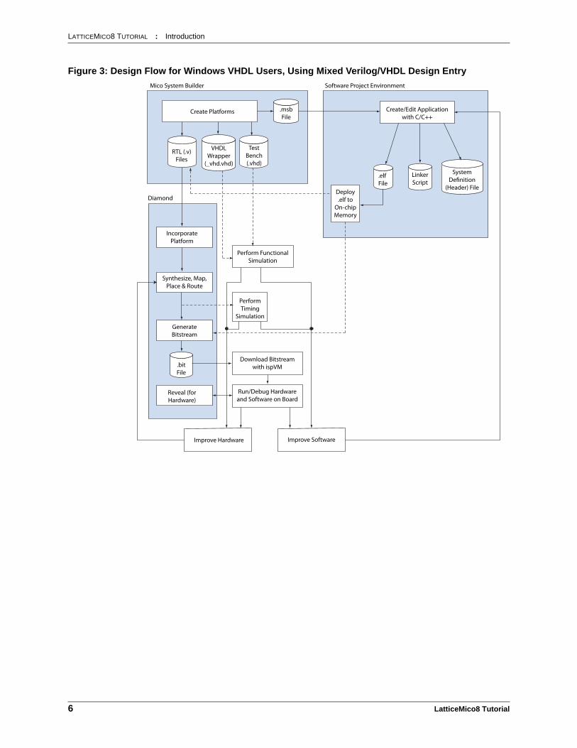
This tutorial supports both Verilog and mixed Verilog/VHDL design flows in Diamond for Windows and Linux users. The Windows Verilog design flow for using LatticeMico System to create an embedded microcontroller and the software code for it is shown in Figure 2. The Windows mixed Verilog/VHDL design flow is shown in Figure 3. The difference between the two methods is that mixed verilog/VHDL designs have a VHDL wrapper as an output from MSB. The VHDL wrapper is an input to Synthesis and Functional Simulation in the Diamond flow.
Functional and timing simulation are performed in third-party and simulation tools outside of Diamond.
GPIO slave device (for controlling LEDs)
UART slave device (for controlling host communication)LM8 CPU
(master ports)
Data port

LATTICEMICO8 TUTORIAL : Introduction
LatticeMico8 Tutorial 5
Figure 2: Design Flow for Windows Verilog Users
Create/Edit Applicationwith C/C++
.elf File
LinkerScript
SystemDefinition
(Header) FileDeploy.elf to
On-chipMemory
Create Platforms
RTL (.v)Files
TestFixture(.v) File
.msbFile
IncorporatePlatform
Synthesize, Map,Place & Route
GenerateBitstream
.bitFile
Reveal (forHardware)
Download Bitstreamwith ispVM
Run/Debug Hardwareand Software on Board
Improve Hardware Improve Software
PerformFunctionalSimulation
PerformTiming
Simulation
Mico System Builder Software Project Environment
Diamond
LATTICEMICO8 TUTORIAL : Introduction
6 LatticeMico8 Tutorial
Figure 3: Design Flow for Windows VHDL Users, Using Mixed Verilog/VHDL Design Entry
Create/Edit Applicationwith C/C++
.elf File
LinkerScript
SystemDefinition
(Header) FileDeploy.elf to
On-chipMemory
Create Platforms
RTL (.v)Files
TestBench(.vhd)
.msbFile
IncorporatePlatform
Synthesize, Map,Place & Route
GenerateBitstream
.bitFile
Reveal (forHardware)
Download Bitstreamwith ispVM
Run/Debug Hardwareand Software on Board
Improve Hardware Improve Software
Perform FunctionalSimulation
PerformTiming
Simulation
VHDLWrapper
(_vhd.vhd)
Mico System Builder Software Project Environment
Diamond

LATTICEMICO8 TUTORIAL : Task 1: Create a New Lattice Diamond Project
LatticeMico8 Tutorial 7
Task 1: Create a New Lattice Diamond Project
As a first step, you will create a new project in Diamond.
To create a new Lattice Diamond project:
1. Create a folder called lm8_tutor in the following directory:
For Windows, <Diamond_install_path>\examples
For Linux, ~/LatticeMico
2. Start Lattice Diamond:
On the Windows desktop, choose Start > Programs > Lattice Diamond > Lattice Diamond.
On the Linux command line, run the following script:<Diamond_install_path>/bin/lin/diamond.
3. Choose File > New > Project, and then click Next in the New Project wizard.
4. In the New Project wizard dialog box, shown in Figure 4, select or specify the following:
a. In the Project Name box, enter platform1.
b. In the Location box, enter the path for the lm8_tutor directory:
For Windows, <Diamond_install_path>\examples\lm8_tutor
For Linux, ~/LatticeMico/lm8_tutor
By default, Diamond uses the Project name and location for the implementation and fills in this information. Although you can change to a different name and directory for the first implementation, you will use the default settings for this tutorial.

LATTICEMICO8 TUTORIAL : Task 1: Create a New Lattice Diamond Project
8 LatticeMico8 Tutorial
Figure 4: New Project Wizard
5. Click Next to proceed to the Add Source dialog box, and then click Next. You will add the source later.
6. In Select Device dialog box, shown in Figure 5, make the following selections:
a. In the Family box, select MachXO2.
b. In the Device box, select LCMXO2-1200HC.
c. In the Speed grade box, select 5.
d. In the Package Type box, select CSBGA132.
e. In the Operating Conditions box, select Commercial.
The dialog box should now resemble the illustration in Figure 5.

LATTICEMICO8 TUTORIAL : Task 1: Create a New Lattice Diamond Project
LatticeMico8 Tutorial 9
Figure 5: New Project Wizard – Select a Device Dialog Box
7. Click Next, and then click Finish.
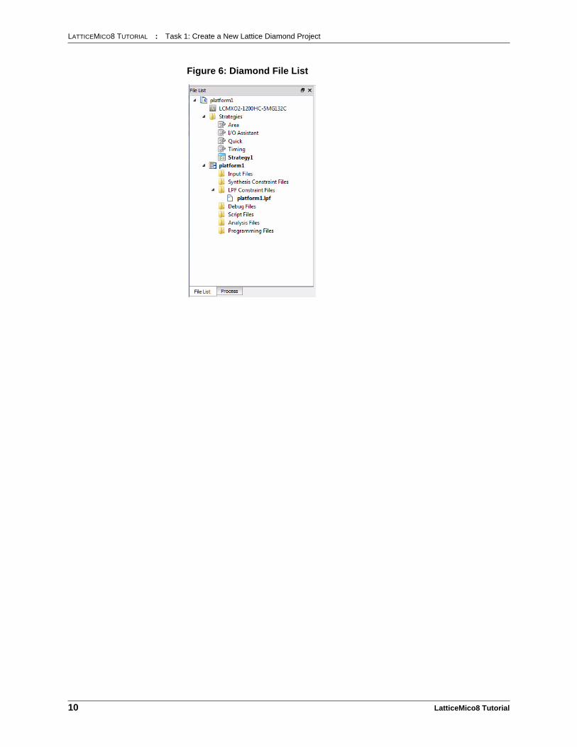
In the File List, shown in Figure 6, the project name is shown at the top. The implementation name, which has the same name as the project name, is displayed in bold type, with the implementation icon . The
project is assigned a default strategy, Strategy1, which is also displayed in bold type with the strategy icon . A strategy is a collection of settings
for logic synthesis, place, and route. You can view these settings by double-clicking the strategy name. The platform1 project is also assigned a logical preference file, platform1.lpf.
LATTICEMICO8 TUTORIAL : Task 1: Create a New Lattice Diamond Project
10 LatticeMico8 Tutorial
Figure 6: Diamond File List
LATTICEMICO8 TUTORIAL : Task 2: Create LatticeMico8 Platform
LatticeMico8 Tutorial 11
Task 2: Create LatticeMico8 Platform
In Task 1, you created a blank Diamond project. The Diamond project is a placeholder for the LatticeMico8 microcontroller platform. You use LatticeMico System Builder (MSB) to create the microcontroller platform. MSB allows you to select components to attach to the microcontroller. Additionally, MSB allows you to customize each of the attached components. After all components are attached to the microcontroller, you use MSB to generate Verilog or VHDL source code that describes a microcontroller–based System-on-a-Chip (SOC). You then enter the HDL source code into the Diamond project in order to create the bitstream used to configure the FPGA.
The steps in this section describe how to build a LatticeMico8 microcontroller SOC that is intended for developing and debugging LatticeMico8-based systems. During system development, the FPGA resources and the firmware are in a state of flux, undergoing many changes. When you deploy a LatticeMico8 microcontroller, as described here, you reduce the impact of the on-going changes in the development environment.
Create a New MSB Platform
Now you will create a new platform in MSB.
To create a new platform:
1. In Windows, from the Start menu, choose Programs > Lattice Diamond > Accessories > LatticeMico System.
For Linux, on the Linux command line, run the following script:
<Diamond_install_path>/micosystem/LatticeMicoLauncher
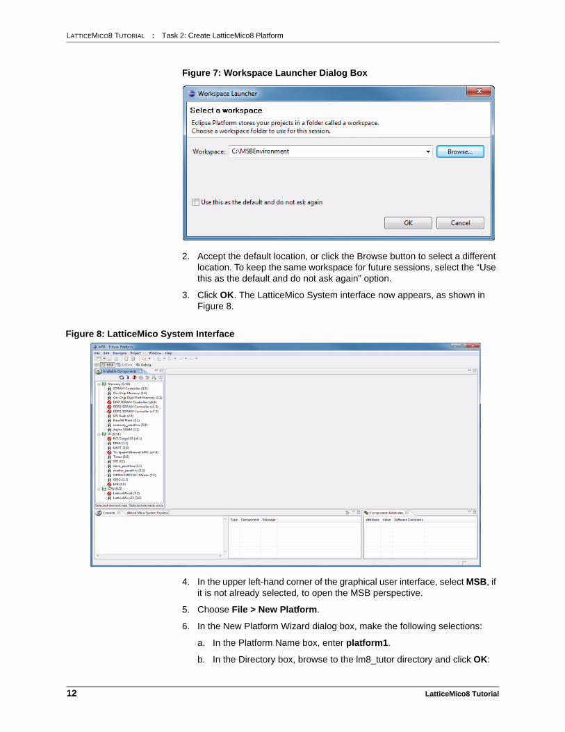
The Workspace Launcher dialog box, shown in Figure 7, displays a default workspace location for the platform.
LATTICEMICO8 TUTORIAL : Task 2: Create LatticeMico8 Platform
12 LatticeMico8 Tutorial
Figure 7: Workspace Launcher Dialog Box
2. Accept the default location, or click the Browse button to select a different location. To keep the same workspace for future sessions, select the “Use this as the default and do not ask again” option.
3. Click OK. The LatticeMico System interface now appears, as shown in Figure 8.
Figure 8: LatticeMico System Interface
4. In the upper left-hand corner of the graphical user interface, select MSB, if it is not already selected, to open the MSB perspective.
5. Choose File > New Platform.
6. In the New Platform Wizard dialog box, make the following selections:
a. In the Platform Name box, enter platform1.
b. In the Directory box, browse to the lm8_tutor directory and click OK:

LATTICEMICO8 TUTORIAL : Task 2: Create LatticeMico8 Platform
LatticeMico8 Tutorial 13
For Windows, <Diamond_install_path>\examples\lm8_tutor
For Linux, ~/LatticeMico/lm8_tutor
c. Do one of the following:
If you are generating a platform in Verilog, leave the Create VHDL Wrapper unselected.
If you are generating a platform in mixed Verilog/VHDL, select only Create VHDL Wrapper.
d. In the Arbitration scheme box, select Shared Bus (Default) from the drop-down menu, if it is not already selected.
e. In the Processor box, select LM8.
f. In the Device Family section, select MachXO2 from the Family menu and All from the Device menu.
g. In the Platform Templates box, select blank.
The New Platform Wizard dialog box should look like the illustration in Figure 9.

LATTICEMICO8 TUTORIAL : Task 2: Create LatticeMico8 Platform
14 LatticeMico8 Tutorial
Figure 9: New Platform Wizard Dialog Box
7. Click Finish.
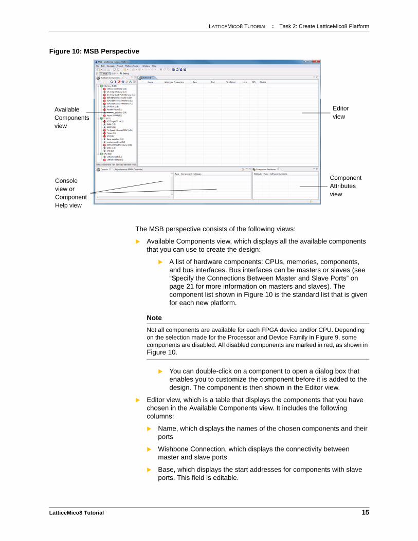
The MSB perspective now appears, as shown in Figure 10.
LATTICEMICO8 TUTORIAL : Task 2: Create LatticeMico8 Platform
LatticeMico8 Tutorial 15
Figure 10: MSB Perspective
The MSB perspective consists of the following views:
Available Components view, which displays all the available components that you can use to create the design:
A list of hardware components: CPUs, memories, components, and bus interfaces. Bus interfaces can be masters or slaves (see “Specify the Connections Between Master and Slave Ports” on page 21 for more information on masters and slaves). The component list shown in Figure 10 is the standard list that is given for each new platform.
You can double-click on a component to open a dialog box that enables you to customize the component before it is added to the design. The component is then shown in the Editor view.
Editor view, which is a table that displays the components that you have chosen in the Available Components view. It includes the following columns:
Name, which displays the names of the chosen components and their ports
Wishbone Connection, which displays the connectivity between master and slave ports
Base, which displays the start addresses for components with slave ports. This field is editable.
Available Components view
Editor view
Component Attributes view
Console view or Component Help view
Note
Not all components are available for each FPGA device and/or CPU. Depending on the selection made for the Processor and Device Family in Figure 9, some components are disabled. All disabled components are marked in red, as shown in Figure 10.

LATTICEMICO8 TUTORIAL : Task 2: Create LatticeMico8 Platform
16 LatticeMico8 Tutorial
End, which displays the end addresses for components with slave ports. This field is not editable. The value of the end address is equivalent to the value of the base address plus the value of the size.
Size (Bytes), which displays the number of addresses available for component access.
Lock, which indicates whether addresses are locked from any assignments. If you lock a component, its address will not change when you select Platform Tools > Generate Address.
IRQ, which displays the interrupt priorities of all components that have interrupt lines connected to the LatticeMico8 microcontroller. The LatticeMico8 microcontroller can accept up to 8 external interrupt lines.
Disable, which indicates whether components are temporarily excluded from the design
Component Help view, which displays information about the component that you selected in the Available Components view. The Help page displays the name of the component—for example, “LatticeMico Timer” or “LatticeMico UART—and gives a brief description of the function of the component. It also provides a list and explanation of the parameters that appear in the dialog box when you double-click the component. If you click the icon next to the component name, you can view a complete description of the component in a PDF file.
Console view, which displays informational and error messages output by MSB
Component Attributes view, which displays the name, parameters, and values of the component selected in the Available Components view or the Editor view. This view is read-only
Add the Microcontroller Core
The first step in building the platform is to add the CPU. In this release, the LatticeMico8 and LatticeMico32 CPUs are available. To add the LatticeMico8 microcontroller core:
1. Under CPU in the Available Components view, click LatticeMico8 to view the information available about the LatticeMico8 microcontroller.
Information about the LatticeMico8 microcontroller, including the parameters that you can set for it, now appears in the Component Help view and in the Component Attributes view in the lower third of the screen. If you click the icon in the Component Help view, you can view the LatticeMico8 Reference Manual, which provides a complete description of the microcontroller.
2. Double-click LatticeMico8 to open the Add LatticeMico8 dialog box. Alternatively, you can select LatticeMico8, and then click the Add Component button .

LATTICEMICO8 TUTORIAL : Task 2: Create LatticeMico8 Platform
LatticeMico8 Tutorial 17
The parameters in the dialog box, shown in Figure 11, correspond to those in the table in the Component Help view.
3. In the Add LatticeMico8 dialog box, do the following:
a. Set the “Number of Registers” to 32.
b. Set the “Call Stack Depth” to 16.
c. Set the address ranges for the Scratchpad and Peripheral (I/O) regions of LatticeMico8.
The maximum size of the two regions is defined by the contents of the field “Data and I/O Addressable Range”. Set this value to 64Kbytes for the tutorial.
The base address of the Scratchpad region is identified by the value in the field “Scratchpad Base Address”. Set this value to 0x00000000 for the tutorial. The software developer can use LatticeMico8 instructions – lsp, lspi, ssp, and sspi – to access this region. The LatticeMico8 compiler will map all of the software application’s data in to this region by default.
The base address of the Peripheral (I/O) region is identified by the value in the field “I/O Base Address”. Set this value to 0x80000000 for the tutorial. This software developer can use LatticeMico8 instructions – import, importi, export, and exporti – or compiler-provided builtin functions –__builtin_export, and __builtin_import – to access this region. Since the LatticeMico8 compiler does not map data accesses in to this region by default, the software developer must explicitly use the aforementioned instructions or functions to direct the compiler to access this region.
d. The LatticeMico8 PROM is either internal to the microcontroller, or located in a non-volatile memory. The following settings determine the PROM settings.
The size of the PROM is defined in the “PROM Size” box and it determines the maximum number of LatticeMico8 instructions that can be stored in it. The size is required regardless of whether the PROM is internal or external. Set this value to 2048 (i.e. 2048 LatticeMico8 assembly instructions).
We need to provide a PROM initialization file that contains the software application’s code image when the PROM is internal. The field “Initialization File Name” will be set up in Task 4.
e. The LatticeMico8 Scratchpad is either internal to the microcontroller, or located in any other volatile memory. The following settings determine the Scratchpad settings.
Select the “Internal Scratchpad” option to locate the Scratchpad within the microcontroller.
Note
In this tutorial the LatticeMico8 PROM is internal. If the developer wants the PROM to reside in non-volatile memory such as SPI flash, he must enable the “Images in Non-Volatile Memory” and “Execute-In-Place” options in the LatticeMico8 configuration GUI.

LATTICEMICO8 TUTORIAL : Task 2: Create LatticeMico8 Platform
18 LatticeMico8 Tutorial
The size of the Scratchpad is defined in the “Scratchpad Size”. The size is required regardless of whether the Scratchpad is internal or external since the LatticeMico8 compiler uses this value to determine the maximum number of bytes that can be within the software application’s data. Set this value to 0x00000800 (i.e. 2046 bytes).
We need to provide a Scratchpad initialization file that contains the software application’s data image when the Scratchpad is internal. The field “Initialization File Name” will be set up in Task 4.
f. Click OK to accept the default settings for the rest of the options. Figure 11 shows the settings that are used for LatticeMico8 within the tutorial.
Figure 11: LatticeMico8 Microcontroller Core Dialog Box
Once you click OK, information about the microcontroller now appears in the Name, Wishbone Connection, Base, End, and Size columns of the table in the Editor view.
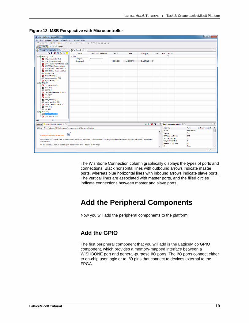
The MSB perspective now shows the LatticeMico8 Microcontroller in the Editor View, as shown in Figure 12.
LATTICEMICO8 TUTORIAL : Task 2: Create LatticeMico8 Platform
LatticeMico8 Tutorial 19
Figure 12: MSB Perspective with Microcontroller
The Wishbone Connection column graphically displays the types of ports and connections. Black horizontal lines with outbound arrows indicate master ports, whereas blue horizontal lines with inbound arrows indicate slave ports. The vertical lines are associated with master ports, and the filled circles indicate connections between master and slave ports.
Add the Peripheral Components
Now you will add the peripheral components to the platform.
Add the GPIO
The first peripheral component that you will add is the LatticeMico GPIO component, which provides a memory-mapped interface between a WISHBONE port and general-purpose I/O ports. The I/O ports connect either to on-chip user logic or to I/O pins that connect to devices external to the FPGA.

LATTICEMICO8 TUTORIAL : Task 2: Create LatticeMico8 Platform
20 LatticeMico8 Tutorial
To add the GPIO to the platform:
1. Under IO in the Available Components view, double-click GPIO. Alternatively, you can select GPIO, then click the Add Component button
.
2. In the Add GPIO dialog box, shown in Figure 13, do the following:
a. In the Instance Name box, change the name of the GPIO to LED. For this tutorial, the GPIO block must be named LED. Failure to name the GPIO block LED will cause mismatches in the FPGA I/O pin names. The example C source code uses this instance name to access the GPIO registers.
b. Change the setting of the Data Width option to 4.
c. Change the setting of the WISHBONE Data Bus Width to 8.
d. Click OK to accept the default settings for the rest of the options.
Figure 13: Add GPIO Dialog Box
Add the UART
The final component that you will add is a LatticeMico universal asynchronous receiver-transmitter (UART), a core that contains a receiver and a transmitter. The receiver performs serial-to-parallel conversion of the asynchronous data frame received at its serial data input pin. The transmitter performs parallel-to-serial conversion on the 8-bit data received from the CPU.

LATTICEMICO8 TUTORIAL : Task 2: Create LatticeMico8 Platform
LatticeMico8 Tutorial 21
To add the UART to the platform:
1. Under IO in the Available Components view, double-click UART to open the dialog box. Alternatively, you can select UART, and then click the Add Component button .
2. In the Add UART dialog box, shown in Figure 14, click OK to accept the default settings.
Figure 14: Add UART Dialog Box.
Specify the Connections Between Master and Slave Ports
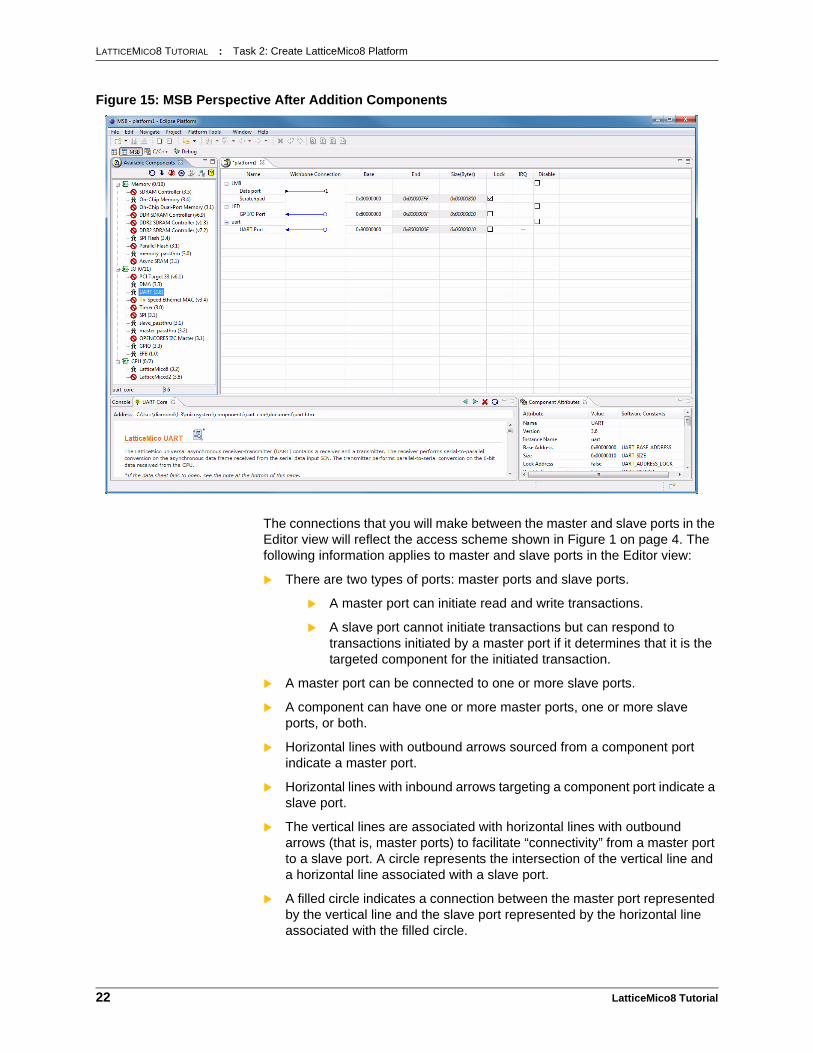
The MSB perspective now resembles the illustration in Figure 15.
LATTICEMICO8 TUTORIAL : Task 2: Create LatticeMico8 Platform
22 LatticeMico8 Tutorial
Figure 15: MSB Perspective After Addition Components
The connections that you will make between the master and slave ports in the Editor view will reflect the access scheme shown in Figure 1 on page 4. The following information applies to master and slave ports in the Editor view:
There are two types of ports: master ports and slave ports.
A master port can initiate read and write transactions.
A slave port cannot initiate transactions but can respond to transactions initiated by a master port if it determines that it is the targeted component for the initiated transaction.
A master port can be connected to one or more slave ports.
A component can have one or more master ports, one or more slave ports, or both.
Horizontal lines with outbound arrows sourced from a component port indicate a master port.
Horizontal lines with inbound arrows targeting a component port indicate a slave port.
The vertical lines are associated with horizontal lines with outbound arrows (that is, master ports) to facilitate “connectivity” from a master port to a slave port. A circle represents the intersection of the vertical line and a horizontal line associated with a slave port.
A filled circle indicates a connection between the master port represented by the vertical line and the slave port represented by the horizontal line associated with the filled circle.

LATTICEMICO8 TUTORIAL : Task 2: Create LatticeMico8 Platform
LatticeMico8 Tutorial 23
A hollow circle indicates an absence of connection between the master port represented by the vertical line and the slave port represented by the horizontal line associated with the hollow circle. This can be seen in Figure 16.
The numbers next to the lines representing the master ports are the priorities in which the master ports can access the slave ports. You can change the priority of these connections by following the instructions in the online Help for LatticeMico System.
To specify the connections between master and slave ports:
1. Connect the data port of the LatticeMico8 microcontroller to the LatticeMico GPIO slave port by clicking the circle in the WISHBONE Connection column of the GPIO Port row.
2. Connect the data port of the LatticeMico8 microcontroller to the LatticeMico UART slave port by clicking the circle in the WISHBONE Connection column of the UART Port row.
Figure 16 shows the resulting connections in the Editor view. This tutorial example uses the shared-bus arbitration scheme. For information about bus arbitration schemes, refer to the “LatticeMico8 Developer's User Guide.”
MSB automatically generates the arbiter, depending on which arbitration scheme is selected. In the case of the shared-bus arbitration scheme, it generates the microcontroller platform to allow multiple master ports access to multiple slave ports over a single shared bus. In the diagram, the data port accesses the LatticeMico GPIO and the LatticeMico UART.

LATTICEMICO8 TUTORIAL : Task 2: Create LatticeMico8 Platform
24 LatticeMico8 Tutorial
Figure 16: Resulting Connections
Assign Component Addresses
The next step is for MSB to generate an address for each component with slave ports. Addresses are specified in hexadecimal notation. Components with master ports are not assigned addresses.
You will not assign individual addresses. To automatically assign component addresses:
Choose Platform Tools > Generate Address, or click the Generate Base Address button , or right-click in the Editor view and choose Generate Address from the pop-up menu. The addresses now appear in the Base and End columns in the Editor view, in hexadecimal notation. Slave components that are not memories are assigned addresses within the 0x80000000-0xFFFFFFFF memory range. The Generate Address command sets A31 of each of the I/O components to ‘1
Note
You can only edit the addresses in the Base column in the Editor View. You cannot edit the addresses in the End column. The value of the end address is equivalent to the value of the base address plus the value of the size.

LATTICEMICO8 TUTORIAL : Task 2: Create LatticeMico8 Platform
LatticeMico8 Tutorial 25
Your MSB perspective should now resemble the example shown in Figure 17. The base addresses that you see in your Editor view might be different from those shown.
Figure 17: MSB Perspective with Component Addresses Assigned
Assign Interrupt Request Priorities
The interrupt request priority is the order in which hardware components request computing time from the CPU. Now you will assign an interrupt request priority (IRQ) to all components that feature a dash in the IRQ column of the Editor view. You cannot assign interrupt priorities to components lacking this dash in the IRQ column, such as memories and CPUs.
Note
Address and size values that appear in italic font in the Editor view cannot be changed.
LATTICEMICO8 TUTORIAL : Task 2: Create LatticeMico8 Platform
26 LatticeMico8 Tutorial
To assign interrupt priorities for all components providing interrupt functionality:
Choose Platform Tools > Generate IRQ, or click the Generate IRQ button , or right-click in the Editor view and choose Generate IRQ from the pop-up menu.
If you accidentally assign duplicate priorities, MSB will issue an error message in the Console view when you select Platform Tools > Generate IRQ.
Perform a Design Rule Check
You will want to perform a design rule check to verify that components in the platform have valid base addresses, interrupt request values, and other fundamental properties.
To perform a design rule check:
Choose Platform Tools > Run DRC, or click the Run DRC button , or right-click in the Editor view and choose Run DRC from the pop-up menu.
In the Console view, MSB shows that there are no errors in the platform.
Generate the LatticeMico8 Platform
You are now ready to generate the microcontroller platform. During the generation process, MSB creates the following files in the “lm8_tutor\platform1\soc” directory:
A platform1.msb file, which describes the platform. It is in XML format and contains the configurable parameters and bus interface information for the components.
A platform1.v (Verilog) file, which is used by both Verilog and mixed Verilog/VHDL users:
For Verilog users, the platform1.v file is used in both simulation and implementation. It instantiates all the selected components and the interconnect described in the MSB graphical user interface. This file is the top-level simulation and synthesis RTL file
Note
To reassign an interrupt priority for a specific component, go to the IRQ column in the row for the component, click on the current interrupt priority number, and choose the new priority number from the drop-down menu. Explicitly assigned interrupt priorities will not be overridden by the interrupt generator tool. The Lock control does not affect IRQ assignment; it only prevents auto-assignment of the Base Address.
LATTICEMICO8 TUTORIAL : Task 2: Create LatticeMico8 Platform
LatticeMico8 Tutorial 27
passed to Diamond. It includes the .v files for each component in the design. These .v files are used to synthesize and generate a bitstream to be downloaded to the FPGA. The first time Generate is run, the Verilog source for each component in the platform, which is located in “<Diamond_install_path>/micosystem/components/<component>”, is copied into a subdirectory called “components”. The components subdirectory is a sibling to the “soc” subdirectory.
For mixed Verilog/VHDL users, the platform1.v file is used in simulation only. A mixed-mode Verilog and VHDL simulator, such as Aldec® Active-HDL™, is needed for functional simulation.
A platform1_vhd.vhd (VHDL) file is created if you selected the “Create VHDL Wrapper” option in the New Platform Wizard dialog box. It is intended to be used only to incorporate the Verilog-based platform into a mixed Verilog/VHDL design. The platform1_vhd.vhd contains the top-level design used for synthesis. This top-level design file instantiates the platform1 component.
A platform1.ngo file, if you selected both the Create VHDL Wrapper and the Create VHDL NGO File options in the New Platform Wizard dialog box. The .ngo file is required for Linux Verilog/VHDL users. It is a synthesized version of platform1.v.
The contents of the platform1.msb file are used by the C/C++ development tools. The C/C++ source code build process extracts the base address information and the size of each component and uses the information to build GNU LD linker files. Each time the Generate function is run, it causes the C/C++ compiler to consider the C/C++ source code to be out of date. This means that the source code will be rebuilt from scratch after each Generate process.
To generate the microprocessor platform:
Click anywhere in the Editor view and choose Platform Tools > Run Generator, or click the Run Generator button , or right-click and choose Run Generator from the pop-up menu.
The Console view displays the output as MSB processes the design. If you are using Verilog, you will see Finish Generator in the Console view when the generator is finished. If the project was created with the “Create VHDL Wrapper” option selected, the project is a mixed Verilog/VHDL flow and the generator silently launches Synplify synthesis and Diamond to create the wrapper. If you are using mixed Verilog/VHDL, you must wait for the Finish VHDL Wrapper message to appear in the Console view.T
he MSB perspective now looks like the illustration in Figure 18. The assigned addresses for the components might differ. As shown in Figure 19, MSB generates a platform1_inst.v file, which contains the Verilog instantiation template for use in a design where the platform is not the top-level module. For a mixed Verilog/VHDL project, no equivalent file is generated.

LATTICEMICO8 TUTORIAL : Task 2: Create LatticeMico8 Platform
28 LatticeMico8 Tutorial
Figure 18: MSB Perspective
Create a User Top-Level Module
As mentioned in the previous section, the platform that is generated by MSB may not be the top-level module. In this scenario, you can use the contents of platform1_inst.v, as shown in Figure 19, within your top-level module. This instantiates the platform generated by MSB within your top-level module.
You must now create a top level file name platform1_top.v to instantiate the MSB-generated platform. Create the file as follows:
Figure 19: platform1_inst.v file
`include "../components/lm8/rtl/verilog/lm8_include_all.v"`include "../components/gpio/rtl/verilog/gpio.v"`include "../components/gpio/rtl/verilog/tpio.v"`include "../components/uart_core/rtl/verilog/uart_core.v"platform1 platform1_u ( .clk_i(clk_i),.reset_n(reset_n), .LEDPIO_OUT(LEDPIO_OUT) // [4-1:0], .uartSIN(uartSIN) // , .uartSOUT(uartSOUT) // );

LATTICEMICO8 TUTORIAL : Task 3: Create Software Application Code
LatticeMico8 Tutorial 29
1. Copy and paste the contents of Figure 20 into a text editor.
2. Name the file platform1_top.v, and save the file in the following directory:
For Windows, <Diamond_install_path>\examples\lm8_tutor\platform1\soc
For Linux, ~/LatticeMico/lm8_tutor/platform1/soc
You will import this file into your Diamond project, in the section ““Importing the Source Files” on page 38.
Task 3: Create Software Application Code
In this task, you create the software application by using C/C++ in the LatticeMico System Software Project Environment (C/C++ SPE). The software application is the code that runs on the LatticeMico8 microcontroller to control the components, the bus, and the memories. The application is written in C.
C/C++ SPE is based on the Eclipse environment and provides an integrated development environment for developing, debugging, and deploying C/C++ applications. C/C++ SPE uses the GNU C tool chain (compiler, assembler, linker, debugger, and other necessary utilities) that has been customized for the LatticeMico8 microcontroller. C/C++ SPE uses the same LatticeMico
Figure 20: User Top Level File
`include "../soc/platform1.v"
module platform1_top (
input reset_n,input uartSIN,output uartSOUT,output [3:0] LEDPIO_OUT
);
// MachX02 internal oscillator generates platform clockwire clk_in;OSCH OSCH_inst (.OSC(clk_in), .SEDSTDBY(), .STDBY(1'b0));defparam OSCH_inst.NOM_FREQ = "24.18";
platform1 platform1_u(
.clk_i (clk_in),
.reset_n (reset_n),
.LEDPIO_OUT (LEDPIO_OUT),
.uartSIN (uartSIN),
.uartSOUT (uartSOUT));
endmodule

LATTICEMICO8 TUTORIAL : Task 3: Create Software Application Code
30 LatticeMico8 Tutorial
System interface as MSB, but it uses a different perspective called the C/C++ perspective.
To activate the C/C++ perspective select C/C++ in the upper left-hand corner of MSB graphical user interface. The C/C++ perspective is shown in Figure 21.
Figure 21: Software Project Environment
The C/C++ perspective consists of the following views:
C/C++ Projects view, which lists C/C++ SPE projects that have been created
Navigator view, which shows all of the file system's files under the workspace directory
Editor view, which is similar to the Editor view in the MSB perspective
Outline view, which displays the structure of the file currently open in the Editor view
Problems view, which displays any error, warning, or informational messages output by C/C++ SPE
Console view, which displays informational messages output by the C/C++ SPE build process
Properties view, which displays the attributes of the item currently selected in the C/C++ Projects view. This view is read-only.
Search view, which displays the results of a search when you choose Search > File.
Tasks view, which shows the tasks running concurrently in the background

LATTICEMICO8 TUTORIAL : Task 3: Create Software Application Code
LatticeMico8 Tutorial 31
Make Targets view, which is not used in LatticeMico8 C projects
Create a New C/C++ SPE Project
You will create a new project in C/C++ SPE, import the platform1.msb file into the project, select the application code template to use so that you do not have to write the code yourself, and compile the code.
To create a new C/C++ SPE project:
1. In the C/C++ perspective, choose File > New > Mico Managed Make C Project.
2. In the New Project dialog box, make the following selections:
a. In the Project Name box, enter LEDTest.
b. In the Location box, browse to the following directory:
For Windows, <Diamond_install_path>\examples\lm8_tutor\platform1
For Linux, ~/LatticeMico/lm8_tutor/platform1
c. In the MSB System box, browse to the following location, select the platform1.msb file in the dialog box, and click Open.
For Windows, lm8_tutor\platform1\soc\platform1.msb
For Linux, lm8_tutor/platform1/soc/platform1.msb
d. In the Select Project Templates box, select LM8 LEDTest as the template for the application code.
The New Project dialog box should resemble the figure shown in Figure 22.
LATTICEMICO8 TUTORIAL : Task 3: Create Software Application Code
32 LatticeMico8 Tutorial
Figure 22: New Project Dialog Box
3. Click Finish.
Now you see the source code in the middle pane of the C/C++ perspective, as shown in Figure 23.
Note
The directory shown in the Location box in the Project Contents field is where the software project directory will be created. Your user files will be placed in this directory.

LATTICEMICO8 TUTORIAL : Task 3: Create Software Application Code
LatticeMico8 Tutorial 33
Figure 23: Source Code in C/C++ Perspective
Build the Project
The next step is to build the project, in which C/C++ SPE compiles, assembles, and links your application code, as well as the system library code provided by C/C++ SPE.
To compile the project:
In the C/C++ Projects view (left-hand pane), select LEDTest and choose Project > Build Project. Do not click on any of the buttons in the Build Project dialog box.
The compilation process generates the following files, among others, in the LEDTest\platform1 directory:
A C header file, DDStructs.h, that describes the device-driver structures for the applicable devices, in addition to the relevant platform settings, such as the microcontroller clock frequency.
A C source file, DDStructs.c, that describes the component instance parameters required by the device drivers in appropriate structures.
A C source file, DDInit.c, that invokes specified device initialization routines for putting the relevant instantiated components in a known state.
A linker script, linker.ld (in LEDTest\platform1\Release), that contains the location and size of the memory components and the rules for generating

LATTICEMICO8 TUTORIAL : Task 4: Deploy Software Application Code to LatticeMico8
34 LatticeMico8 Tutorial
an executable file image, as required by the GNU linker. C/C++ SPE uses this information to ensure that the program code and data are located at the correct addresses. Although it is not covered in this tutorial, the LatticeMico C/C++ SPE enables you to easily specify a custom linker script to be used in lieu of the generated script for the managed build.
A LatticeMico8 software executable linked formal file (.elf). The .elf file contains the LatticeMico8 instructions and information about the pre-initialized data. This tutorial generates a file called platform1.elf.
These files are included within the directory LEDTest and are generated by the C/C++ SPE in the background. All the contents of this directory except user’s C application – in this case it is LEDTest.c – are dynamically generated, and any changes to them are overwritten from build to build. The platform1 library directory (LEDTest\platform1\) contains platform-specific information for the building of an application.
Task 4: Deploy Software Application Code to LatticeMico8
The LEDTest application is in an executable linked format (ELF) that contains both, code and data. This ELF file must be converted in to hexadecimal initialization files, one each for code and data. The initialization file that contains LEDTest code is called prom_init.hex and is used to initialize the LatticeMico8 PROM. The initialization file that contains LEDTest data is called scratchpad_init.hex and is used to initialize the LatticeMico8 Scratchpad.
C/C++ SPE provides an easy-to-use interface for preparing LEDTest for deployment to the LatticeMico8 PROM and Scratchpad. Consult the “LatticeMico8 User Guide” for functional details on the deployment utility.
To prepare LEDTest for deployment:
1. In the C/C++ perspective, select LEDTest and choose Tools > Software Deployment. The Software Deployment Tools dialog box appears, as shown in Figure 24.

LATTICEMICO8 TUTORIAL : Task 4: Deploy Software Application Code to LatticeMico8
LatticeMico8 Tutorial 35
Figure 24: Software Deployment Tools Dialog Box
2. Select Mico8 Memory Deployment, and click on New launch configuration button. The Software Deployment Tools dialog now displays a Mico8 memory deployment configuration settings pane similar to that shown in Figure 26.
a. In the Name box, enter the value LEDTest
b. Browse to LEDTest and select it as the value for the Project box
c. Click on the Search Project button and select LEDTest.elf as the value for the C/C++ Application box
d. Select the folder to which the initialization files are saved.

LATTICEMICO8 TUTORIAL : Task 4: Deploy Software Application Code to LatticeMico8
36 LatticeMico8 Tutorial
Figure 25: Mico8 Configuration Options
3. The configuration options within the Mico8 memory deployment configuration settings pane should look like Figure 26.
Figure 26: Mico8 Memory Deployment Configuration Settings
LATTICEMICO8 TUTORIAL : Task 4: Deploy Software Application Code to LatticeMico8
LatticeMico8 Tutorial 37
4. Click Apply and then click Start.
5. The two initialization files prom_init.mem and scratchpad_init.mem should now be saved within the output folder specified in Step 2.d above.
To initialize LatticeMico8 with LEDTest initialization files:
1. Return to the MSB perspective.
2. Double-click on LM8 instance within the platform.
a. Initialize the PROM in the Initialization File Name box in PROM Settings by browsing to the prom_init.mem file.
b. Initialize the Scratchpad in the Initialization File Name box in Scratchpad Settings by browsing to the scratchpad_init.mem file.
3. The LM8 instance GUI should look like Figure 27. Click OK.
Figure 27: LatticeMico8 Instance GUI
4. Regenerate the hardware platform by clicking anywhere in the Editor view and choose Platform Tools > Run Generator, or clicking the Run Generator button, or right-clicking and choose Run Generator from the pop-up menu.
LATTICEMICO8 TUTORIAL : Task 5: Generate Platform Bitstream
38 LatticeMico8 Tutorial
The LatticeMico8 Verilog source code is now configured to use the prom_init.mem and data_init.mem files that implement LEDTest.
Task 5: Generate Platform Bitstream
The next step in the flow is to generate the microcontroller bitstream. This bitstream is then downloaded to the FPGA on the circuit board. To generate the bitstream, return to Diamond.
Import the MSB Output File
First, you must import the Verilog file output by MSB, the Verilog and VHDL files for mixed Verilog/VHDL, or the EDIF file created by the synthesis tool into Diamond. The process of importing the generated platform file into Diamond is the same for Verilog and mixed Verilog/VHDL, except that you must import the VHDL wrapper file in addition to the Verilog file for mixed Verilog/VHDL.
Configure the Lattice Diamond Environment
The Diamond build process has the ability to operate in two different modes. One is to copy all HDL source files into the Diamond project directory, and the other is to reference them in their current directory structure. The LatticeMico8 build requires that the source files remain in the directory structure created by MSB. The default Diamond behavior is to leave the files where they are, but it is advisable to verify that Diamond is configured correctly.
1. In Diamond, choose Tools > Options.
2. Under Environment, in the left pane of the Options dialog box, select General.
3. If the option Copy file to Implementation's Source directory when adding existing file is selected, clear this option and click OK.
Importing the Source Files
You import the top-level file, platform1_top.v, into Diamond. To import the Verilog or Verilog/VHDL files for the tutorial example:
1. In Diamond, choose File > Add > Existing File.
2. In the dialog box, browse to the directory containing the top level Verilog source code.
For Windows, <Diamond_install_path>\examples\lm8_tutor\platform1\soc
For Linux, ~/LatticeMico/lm8_tutor/platform1/soc/

LATTICEMICO8 TUTORIAL : Task 5: Generate Platform Bitstream
LatticeMico8 Tutorial 39
3. Do one of the following:
Select the platform1_top.v file (Verilog), and click Add.
If your design is mixed Verilog/VHDL, select the platform1_top.v, and the platform1_vhd.vhd files and click Add.
4. If your design is mixed Verilog/VHDL, perform the following additional steps:
a. Choose Project > Property Pages.
b. In the dialog box, select the project name that appears in bold type next to the implementation icon .
c. In the right pane, click inside the Value cell for “Top-Level Unit” and select platform1_top from the drop-down menu.
d. Click inside the Value cell for “Verilog Include Search Path,” and then click the browse button to open the “Verilog Include Search Path” dialog box.
e. In the dialog box, click the New Search Path button , browse to the <platform1>\soc directory, and click OK.
f. Click OK to add the path to the Project Properties and close the “Verilog Include Search Path” dialog box.
g. Click OK to return to the Diamond main window.
Connect the Microcontroller to the FPGA Pins
You have two options for connecting the microcontroller to the FPGA pins:
Manually create the pin constraints and import them into Diamond.
Import a preconfigured preference file into Diamond.
For this tutorial, you will import a preconfigured pin preference file into Diamond. Create a preconfigured pin preference file named “untitled.lpf” as follows:
1. Copy and paste the contents of Figure 28 into a text editor.
2. Name the file untitled.lpf, and save the file in the following directory:
For Windows, <Diamond_install_path>\examples\lm8_tutor
For Linux, ~/LatticeMico/lm8_tutor/
To import this preconfigured pin preference file:
1. In Diamond, select the File List tab and double-click Strategy1.
2. In the Strategies dialog box, select Translate Design in the left pane.
3. In the right pane, double-click the cell in the Value column for Consistent Bus Name Conversion.

LATTICEMICO8 TUTORIAL : Task 5: Generate Platform Bitstream
40 LatticeMico8 Tutorial
4. Choose Lattice from the drop-down menu, and click OK.
5. In Diamond, choose File > Add > Existing File.
6. In the Add Existing File dialog box, do the following:
a. Select Constraint Files (*.lpf) from the Files of type menu.
b. Select the option Copy file to Implementation’s Source directory.
c. Navigate to the directory containing the untitled.lpf file for the File Name box, and click Add. Diamond adds the .lpf file to the project and displays file name and path in the File List.
7. In the File List pane, right-click untitled.lpf and choose Set as Active Preference File.
8. Diamond displays the untitled.lpf file and path in bold type, indicating that the untitled.lpf will now be used instead of the platform1.lpf file.
Perform Functional Simulation
You can optionally simulate the functionality of the output top-level platform1.v or platform1_vhd.vhd module by using a simulator such as Active-HDL in Diamond. See the Active-HDL online Help in Diamond for more information on this procedure.
Figure 28: Preconfigured Pin Preference File
AUTOMOTIVE ;BLOCK RESETPATHS ;BLOCK ASYNCPATHS ;BLOCK INTERCLOCKDOMAIN PATHS ;
LOCATE COMP "reset_n" SITE "K2" ;IOBUF PORT "reset_n" IO_TYPE=LVCMOS18 ;#-----------------------------------------------------------# LEDs assumes the component instance name is LED & has# a width of 4#-----------------------------------------------------------LOCATE COMP "LEDPIO_OUT_0_" SITE "F1" ;LOCATE COMP "LEDPIO_OUT_1_" SITE "F2" ;LOCATE COMP "LEDPIO_OUT_2_" SITE "F3" ;LOCATE COMP "LEDPIO_OUT_3_" SITE "H2" ;IOBUF PORT "LEDPIO_OUT_0_" IO_TYPE=LVCMOS18 ;IOBUF PORT "LEDPIO_OUT_1_" IO_TYPE=LVCMOS18 ;IOBUF PORT "LEDPIO_OUT_2_" IO_TYPE=LVCMOS18 ;IOBUF PORT "LEDPIO_OUT_3_" IO_TYPE=LVCMOS18 ;#-----------------------------------------------------------# UART assumes the component instance name is uart#-----------------------------------------------------------LOCATE COMP "uartSIN" SITE "H1" ;LOCATE COMP "uartSOUT" SITE "H3" ;IOBUF PORT "uartSIN" IO_TYPE=LVCMOS18 ;IOBUF PORT "uartSOUT" IO_TYPE=LVCMOS18 ;BLOCK JTAGPATHS;

LATTICEMICO8 TUTORIAL : Task 6: Download Platform Bitstream to FPGA
LatticeMico8 Tutorial 41
For Verilog simulation, you use platform1.v and all the Verilog files for each attached component.
For mixed Verilog/VHDL simulation, you use platform1_vhd.vhd, platform1.v, and all the Verilog files for each attached component. You must use a mixed-language simulator such as ModelSim® SE or Aldec Active-HDL.
Perform Timing Simulation
You can optionally validate the timing of your design by performing timing simulation. Because timing simulation is a complex topic, it is not addressed in this tutorial. For information on timing simulation, see the Achieving Timing Closure in FPGA Designs Tutorial, the “Design Verification” topic in the Diamond online Help, or the “Strategies for Timing Closure” chapter of the FPGA Design Guide.
The timing simulation process automatically builds a database and maps, places, and routes the design.
Generate the Bitstream
Now you will generate a bitstream to download the microprocessor platform to the FPGA. If you did not perform timing simulation, the bitstream generation process will automatically synthesize, map, place, and route the design before it generates the bitstream.
To generate a bitstream:
1. In Diamond, select the Process tab.
2. In the Export Files section, double-click JEDEC File.
Diamond now generates a bitstream, platform1_platform1.jed, that is ready to be downloaded into the device. This process takes several minutes.
Task 6: Download Platform Bitstream to FPGA
The bitstream generated in the previous section contains all the information required to program the MachXO2 FPGA. Diamond Programmer sends the programming bitstream to the FPGA over a parallel port or USB port communications link.
Now you will use Programmer to download the hardware bitstream that you generated in the previous section to the FPGA on the board.

LATTICEMICO8 TUTORIAL : Task 6: Download Platform Bitstream to FPGA
42 LatticeMico8 Tutorial
To download the bitstream to the FPGA on the board:
1. Remove any Lattice USB Programming cables from your system.
2. Connect the power supply to the development board.
3. Connect a USB cable from your computer to the MachXO2 Control Board. The USB cable must be connected to the USB target connector adjacent to the keypad. Give the computer a few seconds to detect the USB device on the MachXO2 Control board before moving to step 4.
4. In Diamond, choose Tools > Programmer.
5. In the Getting Started dialog box, choose Create a new Blank Project. Leave the Import File to Current Implementation box checked, and click OK. Programmer scans the device database, and then the Programmer view displays in Diamond.
6. In the Cable Settings dialog box on the right side of the Programmer window, do the following:
a. In the Cable box, select USB2.
b. In the Port box, choose the only setting available in the drop-down menu, FTUSB-0.
7. Double-click the File Name column. Click to display the Open File dialog box, and browse to the platform1_platform1.jed file in the following directory:
For Windows, <Diamond_install_path>\examples\lm8_tutor\platform1_platform1.jed
For Linux, ~/LatticeMico/lm8_tutor/platform1_platform1.jed
8. Click Open.
9. Double-click the Operation column to display the Device Properties dialog box, as shown in Figure 29, and choose the following settings:
For Access Mode, choose Flash Programming Mode from the pull-down menu.
For Operation, choose Flash, Erase, Program, Verify from the pull-down menu.

LATTICEMICO8 TUTORIAL : Task 6: Download Platform Bitstream to FPGA
LatticeMico8 Tutorial 43
Figure 29: Device Properties Dialog Box.
10. Click OK.
11. The Programmer view should look as shown in Figure 30.
Figure 30: Diamond Programmer
12. Click the Program button on the Programmer toolbar to initiate the download.
13. Check the Programmer output console to see if the download passed, as shown in Figure 31. If the programming process succeeded, you will see a green-shaded PASS in the Programmer Status column.

LATTICEMICO8 TUTORIAL : Summary
44 LatticeMico8 Tutorial
Figure 31: Programmer Output Console
14. At the end of this process, the FPGA is loaded with the microcontroller hardware configuration. If the design is successfully downloaded onto the MachXO2 device, the four LEDs on the MachXO2 Control Board should blink in sequence and repeat the pattern.
15. In Diamond, choose File > Save. In the Save .xcf File As dialog box, enter platform1.xcf in the File Name box, and click Save.
Summary
You have finished the LatticeMico8 Tutorial. In this tutorial, you have learned how to do the following:
Set up a Lattice Diamond FPGA project.
Create microcontroller platform for the LatticeMico8 embedded microcontroller in MSB.
Create the software application code for the microcontroller platform with C/C++ SPE.
Deploy the software application code to the microcontroller’s internal PROM and Scratchpad.
Generate a bitstream of the microcontroller platform in Diamond.
Download the hardware bitstream to the FPGA on the board using Diamond Programmer.


