35
LOGICAL DESIGN 2 Course titular: DUMITRAŞCU Eugen

LOGICAL DESIGN 2
Course titular:DUMITRAŞCU Eugen
PROGRAMMABLE LOGIC DEVICES
CHAPTER 6

29-May-19 LD2_06 2018-2019 3
CONTENT
General presentation SPLD (Simple Programmable Logic
Devices) CPLD (Complex Programmable Logic
Devices) FPGA (Field Programmable Gate
Array)

29-May-19 LD2_06 2018-2019 4
GENERAL PRESENTATION
The disadvantages of implementing the interconnection of integrated circuits in SSI/MSI are:
large amount of implementation; high energy consumption; great heat dissipation; very large number of interconnections; relatively low speed work due to the length of external
connections and solder points; the reliability decreases proportionally with increasing
complexity; big allocated time for design by classical methods; testing and debugging are difficult.
29-May-19 LD2_06 2018-2019 5
GENERAL PRESENTATION
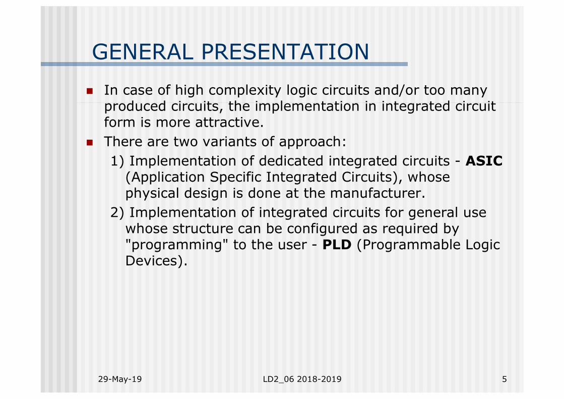
In case of high complexity logic circuits and/or too many produced circuits, the implementation in integrated circuit form is more attractive.
There are two variants of approach:1) Implementation of dedicated integrated circuits - ASIC
(Application Specific Integrated Circuits), whose physical design is done at the manufacturer.
2) Implementation of integrated circuits for general use whose structure can be configured as required by "programming" to the user - PLD (Programmable Logic Devices).
29-May-19 LD2_06 2018-2019 6
GENERAL PRESENTATION
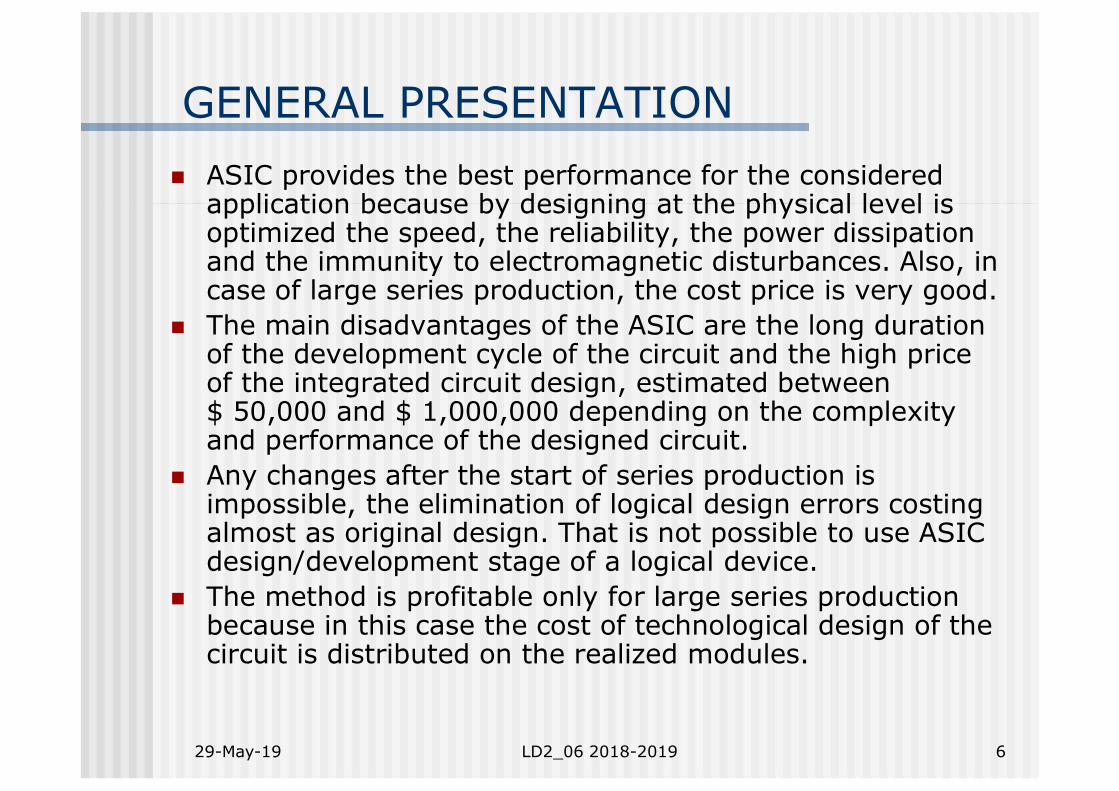
ASIC provides the best performance for the considered application because by designing at the physical level is optimized the speed, the reliability, the power dissipation and the immunity to electromagnetic disturbances. Also, in case of large series production, the cost price is very good.
The main disadvantages of the ASIC are the long duration of the development cycle of the circuit and the high price of the integrated circuit design, estimated between $ 50,000 and $ 1,000,000 depending on the complexity and performance of the designed circuit.
Any changes after the start of series production is impossible, the elimination of logical design errors costing almost as original design. That is not possible to use ASIC design/development stage of a logical device.
The method is profitable only for large series production because in this case the cost of technological design of the circuit is distributed on the realized modules.

29-May-19 LD2_06 2018-2019 7
GENERAL PRESENTATION
PLDs have a very general structure, configurable to the user and have been introduced in the mid `70s in order to provide highly flexible integrated circuits in utilization with a reasonable cost price.
It is necessary to distinguish between using of the term "programming" in software and hardware. In the first case a program is loaded and run on hardware with a well defined structure while the second case involves configuring of the circuit at the physical level.
The first PLDs were called PAL (Programmable Array Logic) respectively PLA (Programmable Logic Array). They use only AND and OR logic gates allowing only implementing CLC with medium complexity.
Very soon this limitation was removed by including in a single module of a PAL/PLA structure with one flip-flop for each output, ensuring the implementation in single module of some simple SLC.

29-May-19 LD2_06 2018-2019 8
GENERAL PRESENTATION
In the early `80s have been introduced so-called macrocells, which include a flip-flop, logic gates and multiplexers. The structure of a macrocell is programmable allowing to implement several working regimes.
The devices whose output is provided with a macrocell subsequently received the name GAL (Generic PAL). Sometimes it is used the name of PALCE (PAL CMOS Electrically erasable/programmable).
Currently the type circuits PAL, PLA, GAL are referenced in the literature as SPLDs (Simple PLDs). In fact, as an independent integrated circuit are produced only GAL/PALCE.
An important step is the transition to production of some circuits with more GALs on the same silicon chip. These circuits have auxiliary logic for interconnecting GALs but also to provide additional facilities. Such circuits have been named CPLD (Complex PLD) and became popular due to good performance at low cost (even under $ 1).

29-May-19 LD2_06 2018-2019 9
GENERAL PRESENTATION
Also in the mid `80s were introduced the circuits called FPGA (Field Programmable Gate Array), with a totally different structure of SPLD and CPLD. They are widely used to implement circuits with high complexity and high performance.
A summary of the evolution and classification of PLD is presented in table bellow:
PLD
SPLD
PAL
PLA
PAL/PLA with FF
GAL
CPLD
FPGA
29-May-19 LD2_06 2018-2019 10
CONTENT
General presentation SPLD (Simple Programmable Logic
Devices) CPLD (Complex Programmable Logic
Devices) FPGA (Field Programmable Gate
Array)

29-May-19 LD2_06 2018-2019 11
SPLDPLA structure PLA (Programmable Logic Array) consists of an AND gates
area and an OR gates area, each programmable.A0A2A3 A1
4
4
4
4
4
4
4
4
4
m m
O0 O3O2O1
m
O4
m m

29-May-19 LD2_06 2018-2019 12
SPLD Each variable appears inside the circuit both in direct and
complemented form. Each AND gate can generate a P term (not necessarily a
minterm as a memory case) depending on variables that are connected on inputs gate.
Each OR gate represents a function. A P term can be attached to many functions necessary. Such this structure is flexible but complex at the same
time, resulting an high cost per module and low work speed.
From this reason such circuits is no longer manufactured now.
29-May-19 LD2_06 2018-2019 13
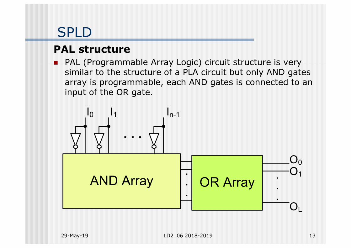
SPLDPAL structure PAL (Programmable Array Logic) circuit structure is very
similar to the structure of a PLA circuit but only AND gates array is programmable, each AND gates is connected to an input of the OR gate.
AND Array OR Array...
. . .
I0 In-1I1
O0
OL
O1...

29-May-19 LD2_06 2018-2019 14
SPLD This loss of flexibility in using circuits has allowed obtaining
some circuits with an attractive cost price and a very good work speed.
The flexibility in use was increased primarily by adding additional control circuits of outputs.
In the next figure is shown the detailed structure of a hypothetical PAL.
XOR gates work as a commanded inverter.

29-May-19 LD2_06 2018-2019 15
SPLD
O1
O3
O2
x0 x1 x2 x5x4x3 x6 CE
29-May-19 LD2_06 2018-2019 16
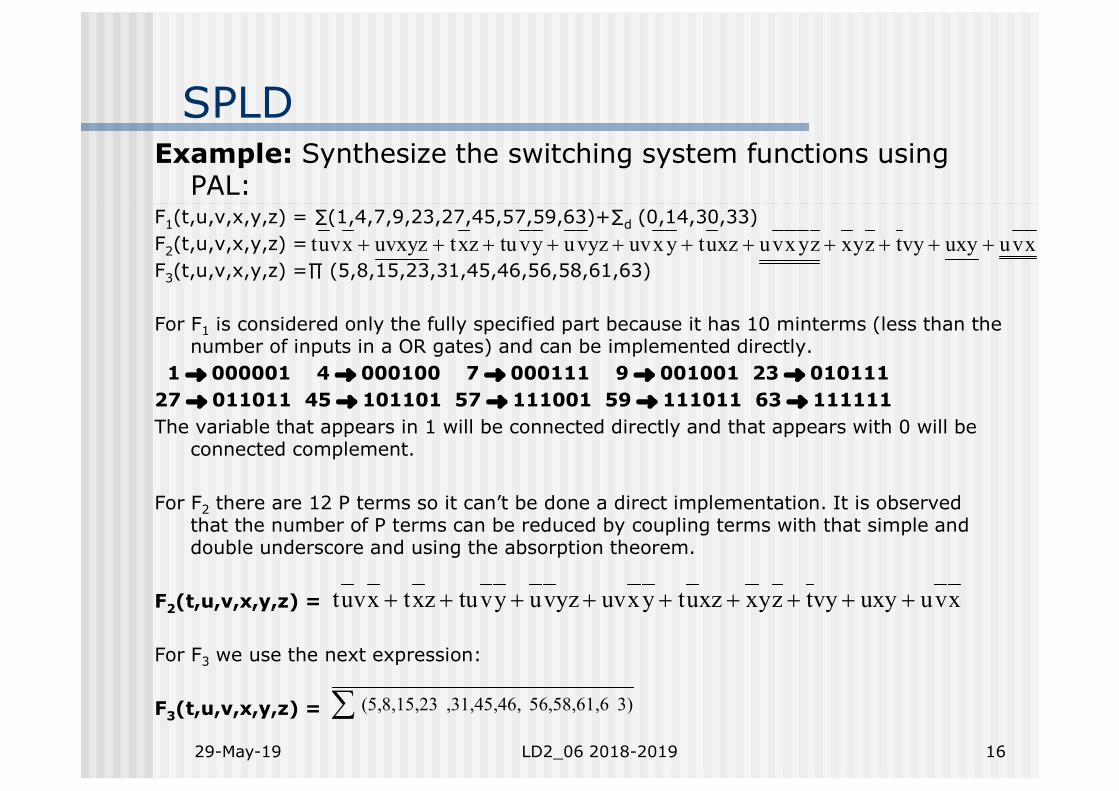
SPLDExample: Synthesize the switching system functions using
PAL: F1(t,u,v,x,y,z) = ∑(1,4,7,9,23,27,45,57,59,63)+∑d (0,14,30,33)F2(t,u,v,x,y,z) = F3(t,u,v,x,y,z) =∏ (5,8,15,23,31,45,46,56,58,61,63)
For F1 is considered only the fully specified part because it has 10 minterms (less than the number of inputs in a OR gates) and can be implemented directly.
1 000001 4 000100 7 000111 9 001001 23 010111 27 011011 45 101101 57 111001 59 111011 63 111111The variable that appears in 1 will be connected directly and that appears with 0 will be
connected complement.
For F2 there are 12 P terms so it can’t be done a direct implementation. It is observed that the number of P terms can be reduced by coupling terms with that simple and double underscore and using the absorption theorem.
F2(t,u,v,x,y,z) =
For F3 we use the next expression:
F3(t,u,v,x,y,z) =
xvuuxyvytzyxzyxvuxzutyxuvyzvuyvtuzxtuvxyzxvut
xvuuxyvytzyxxzutyxuvyzvuyvtuzxtxvut
3)56,58,61,6,31,45,46,(5,8,15,23

29-May-19 LD2_06 2018-2019 17
SPLD
F1
F3
F2
t u v zyx NC

29-May-19 LD2_06 2018-2019 18
SPLD A major improvement of PALs was the introduction of some
macrocells that allow more working regimes. Basically a macrocell is formed by a flip-flop, multiplexers
and buffer circuits with tri-state outputs. The modern PAL circuits are made in EPROM technology,
and contain programmable macrocells. Such circuits known as GAL circuits and have been
introduced by Lattice Semiconductor Company.

29-May-19 LD2_06 2018-2019 19
SPLDPAL CE22V10 – block diagram

29-May-19 LD2_06 2018-2019 20
SPLDPAL CE22V10 – macrocell

29-May-19 LD2_06 2018-2019 21
SPLDPAL CE22V10 – working regimes

29-May-19 LD2_06 2018-2019 22
SPLDPAL CE22V10 – principle scheme

29-May-19 LD2_06 2018-2019 23
SPLDPAL CE22V10 – detail
29-May-19 LD2_06 2018-2019 24
CONTENT
General presentation SPLD (Simple Programmable Logic
Devices) CPLD (Complex Programmable Logic
Devices) FPGA (Field Programmable Gate
Array)

29-May-19 LD2_06 2018-2019 25
CPLD CPLD (Complex PLD) – extends the concept of PLD to a
higher level of integration, which the result improve the performances: increase the efficiency in using silicon chips; increase the reliability of schemes; decreases the cost price; reduce the complexity of implementations; decrease the gauge (dimension); increase the speed of work; reduce the life cycle of the projects.
A CPLD contains several logical blocks, similar in structure with PAL 22V10, which communicates with each other by signals routed through a programmable interconnection block (PIB).

29-May-19 LD2_06 2018-2019 26
CPLDCPLD – block diagram
Logic block
Logic block
Logic block
Logic block
Logic block
Logic block
Logic block
Logic block
Pro
gra
mm
ab
le i
nte
rco
nn
ec
tio
n b
lock
I/O
I/O

29-May-19 LD2_06 2018-2019 27
CPLDCPLD – detailed block diagram
BIPPIB I/O
Logic block
P terms array P terms distributor
Macrocell
Mcell
29-May-19 LD2_06 2018-2019 28
CONTENT
General presentation SPLD (Simple Programmable Logic
Devices) CPLD (Complex Programmable Logic
Devices) FPGA (Field Programmable Gate
Array)
29-May-19 LD2_06 2018-2019 29
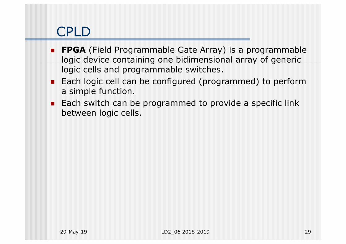
CPLD FPGA (Field Programmable Gate Array) is a programmable
logic device containing one bidimensional array of generic logic cells and programmable switches.
Each logic cell can be configured (programmed) to perform a simple function.
Each switch can be programmed to provide a specific link between logic cells.

29-May-19 LD2_06 2018-2019 30
CPLDFPGA – block diagram
29-May-19 LD2_06 2018-2019 31
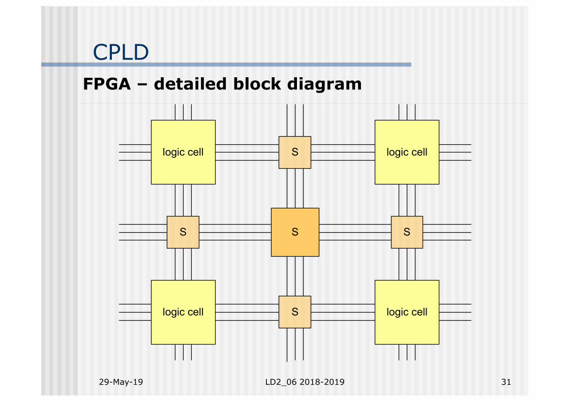
CPLDFPGA – detailed block diagram
logic cell S logic cell
logic cell S logic cell
S SS
29-May-19 LD2_06 2018-2019 32
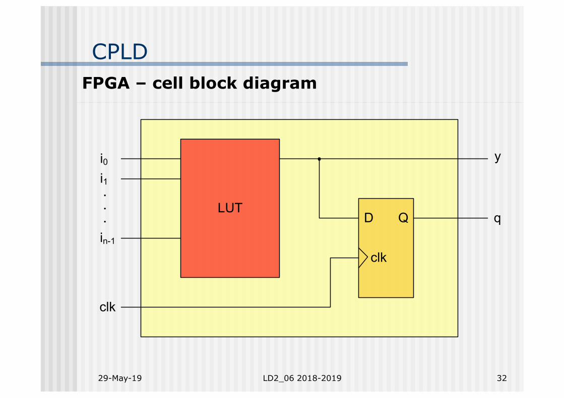
CPLDFPGA – cell block diagram
LUT
y
qD Q
clk
clk
i0
in-1
i1...

29-May-19 LD2_06 2018-2019 33
CPLDFPGA – programmable cell – XC4000 series
29-May-19 LD2_06 2018-2019 34
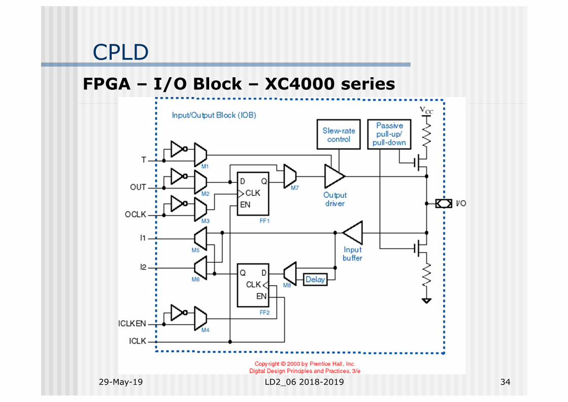
CPLDFPGA – I/O Block – XC4000 series

QUESTIONS?


