SOLDER SPREAD: A CRITERION FOR EVALUATION OF SOLDERING G. Humpston D. M. Jacobson Metallurgical Technology Group GEC Hirst Research Centre Wembley UK Quantitative measurements of the intrinsic spread characteris- tics of solders used in electronics applications can be carried out by making use of the beneficial properties of gold. I t is well known that some solders flow and spread more readily than others and is widely held that eutectic composition alloys are usually the most fluid, that is they exhibit a relatively high degree of spread [1,2] . Indeed, this is one of the main reasons why solders tend to be based on eutectic alloys [3]. Another reason is that solders of eutectic composition transform from liquid to solid at a single temperature rather than over a finite temperature range. The most widely used solder, of the Pb-60wt.%Sn composition, embodies both of these features. Restricted flow is generally regarded as being indicative of a poor joint, caused by factors such as dewetting, oxidation of the components or the sub- strate temperature being too low. High fluidity of molten solders is a desirable prop- erty where the filler metal is applied as a slug of wire to one edge of a heated assembly and expected to flow into the joint by capillary action. However, there are other situations where it is both possible and more convenient to sandwich a foil of the solder between the components which are then joined together in an appropriate heat- ing cycle. When this configuration is used, a high degree of solder spread might actually be detrimental to good joint filling because the molten alloy will tend to flow out of the joint. Therefore, there is also a requirement for solders that possess low spread characteristics, even when all surfaces are perfectly clean and wettable by the molten solder. Gold Bull., 1990, 23 (3) 83
Transcript
SOLDER SPREAD:A CRITERION FOR
EVALUATION OF SOLDERING
G. Humpston
D. M. Jacobson
Metallurgical Technology GroupGEC Hirst Research Centre
Wembley UK
Quantitative measurements of the intrinsic spread characteris-tics of solders used in electronics applications can be carried outby making use of the beneficial properties of gold.
I t is well known that some solders flow and spreadmore readily than others and is widely held that
eutectic composition alloys are usually the most fluid,that is they exhibit a relatively high degree of spread[1,2] . Indeed, this is one of the main reasons why solderstend to be based on eutectic alloys [3]. Another reasonis that solders of eutectic composition transform fromliquid to solid at a single temperature rather than overa finite temperature range. The most widely used solder,of the Pb-60wt.%Sn composition, embodies both ofthese features. Restricted flow is generally regarded asbeing indicative of a poor joint, caused by factors suchas dewetting, oxidation of the components or the sub-strate temperature being too low.
High fluidity of molten solders is a desirable prop-erty where the filler metal is applied as a slug of wire toone edge of a heated assembly and expected to flow intothe joint by capillary action. However, there are othersituations where it is both possible and more convenientto sandwich a foil of the solder between the componentswhich are then joined together in an appropriate heat-ing cycle. When this configuration is used, a high degreeof solder spread might actually be detrimental to goodjoint filling because the molten alloy will tend to flowout of the joint. Therefore, there is also a requirementfor solders that possess low spread characteristics, evenwhen all surfaces are perfectly clean and wettable by themolten solder.
Gold Bull., 1990, 23 (3) 83
To date, there is little published data comparing thespread characteristics of different solders and relatingthis property to their propensity to fill joints. Thisdearth of quantitative information can be attributedlargely to the lack of a suitable substrate on which tobase objective comparisons of solder flow and jointfilling. An "ideal" substrate would have to fulfil a num-ber of requirements. In particular it would need to be:
• readily wetted by all molten solders, without theaid of fluxes which might introduce spurious ef-fects;
• essentially inert, from a metallurgical point of view,so that wetting by the solder would neither modifythe balance of phases present in the solder, nor itsphysical characteristics;
• stable against exposure to the atmosphere so thatthe substrate would have a reasonably long solder-ability "shelf-life" for carrying out reproducibletests;
• easy and cheap to fabricate to a consistent quality.
Failure to satisfy any of these requirements restrictsthe relevance of the published data on solder spreadbeyond the particular combination of materials andprocesses examined. This study identifies an "ideal"substrate which satisfies all of the above criteria, withincertain limits. It then describes how this substrate wasused to derive comparative solder spread data for aselection of binary alloy solders, comprising all combi-nations of the elements bismuth, indium, lead, silverand tin. The spread data is then compared and con-trasted and the differences analysed.
A companion article will extend the study to assess-ing the relationship between solder spread andhermeticity of joints made using solder preforms.
Developmentof an"Ideal" Substrate
In order for a molten alloy to wet a metallic substrate inthe absence of fluxes, it is generally necessary for thesurface of the substrate to be completely free of anynon-wettable surface films such as organic residues and
oxides. Noble metals such as platinum and gold areunreactive towards ambient atmospheres and to sol-vents used for degreasing. These metals are thereforesolderable even without fluxes being present and, onthat account, are suitable candidates for the requiredsolder test substrates. Gold was selected in preference toplatinum precisely because it is widely used in flux-freesoldering applications [4].
However, gold is highly soluble in most commonsolders and the resulting alloying alters their metallur-gical and physical characteristics [4,5,6,7] , An exceptionto this trend is provided by some of the indium-basedsolders. These alloys react with gold to form an interfa-cial layer of the AuIn2 intermetallic compound [4],Once established, this layer tends to inhibit furtherinteraction between the gold layer and the molten sol-der, thereby preventing the dissolution of gold by thesolder reaching a level where it significantly modifies themetallurgical characteristics of the latter.
One obvious means of limiting the dissolution ofgold in solders is to restrict the volume of this metal toa thin surface coating. If this coating is made sufficientlythin, relative to the volume of solder, it will not appre-ciably affect the characteristics of the solder. The rele-vant data on maximum concentrations of gold in vari-ous solders that will assure compliance with this condi-tion have been published [4], At the other extreme,there is a minimum limit to the gold coating thickness,namely that which is capable of providing an adequatesolderability shelf-life. Data relating gold thickness toshelf-life was not available from the literature and hadto be obtained as a preliminary step to this study. Thiswork is described in the following section.
Because the thin gold layer envisaged was consid-ered likely to completely dissolve in most of the moltensolders, an underlying metallic layer is required andtherefore has to form an essential part of the substrate.The candidate metal would be protected from the at-mosphere by the gold overlay, prior to the applicationof the solder, so that its reactivity with the ambientatmosphere was not a consideration in the choice. How-ever, it is necessary that a clean surface of this metal isreadily wetted by molten solders while, at the same time,it is essentially insoluble in these alloys. A 0.1 µm thicklayer of chromium, applied by sputter-deposition to aglass substrate, has been found by previous experienceat the GEC Hirst Research Centre to satisfy this require-ment. Once deposited, the chromium layer must be
84 Gold Bull., 1990, 23 (3)
immediately coated with gold, without breaking thevacuum, in order to ensure that it does not oxidise.
The adoption of a standard glass substrate of knownflatness was deliberate, because surface roughness isknown to influence the rate of reaction between soldersand substrates [8,9]. This is presumably associated insome manner with the increase in surface area thataccompanies increasing surface roughness. It was possi-ble to use glass as the bulk substrate, even though it isnot wetted by solders, because it is covered with the layerof chromium which is insoluble in most solders. Thechromium-on-glass combination also enables any dis-solution of the chromium by a solder to be detectedvisually from the underside of the substrate.
Metals such as nickel, titanium, molybdenum andtungsten, all of which are routinely deposited by vapourphase processes, were considered as possible alternativesto chromium. However, all of these metals react withone or more of the constituents of common solderalloys. Thus, for example, nickel dissolves in silver,titanium in indium and tin, while tungsten and moly-bdenum dissolve in molten lead.
Sputtering is frequently chosen for applying thinmetallisation layers to substrates because this vapourdeposition technique is capable of doing so in a highlycontrollable and reproducible manner. Moreover, thelayers can be deposited with a high density and lowporosity, as compared with electroplating. Sputtering isalso amenable to multilayer deposition and it offers thepossibility of cleaning surfaces by reverse sputtering, orsputter etching, prior to commencing the depositionand so ensures excellent adhesion of the coatings to thebase material. These features made sputtering a naturalchoice as the technique to use for preparing the "ideal"substrates.
Assessment of theShelf-life SolderabilityProvided byThin Gold CoatingsThe following programme of work was undertaken inorder to establish the solderability shelf-life characteris-tics of sputtered gold coatings as a function of theirthickness. For comparative purposes, gold coatings ap-
plied by wet plating methods were assessed in parallel,because these are widely used in industry, their beinghighly amenable to mass fabrication.
Experimental ProcedureThe substrates for assessment of the shelf-life of elec-troplated gold coatings were based on coupons of cop-per, a metal that is widely used as a substrate for solderedjoints. The coupons, which measured 15 x 10 x0.15 mm, were chemically cleaned and then immedi-ately electroplated with either 0.1, 1 or 5 µm of gold.
Glass specimens with the same surface dimensions,but 1.1 mm thick, were cut from microscope slides andused as the substrates for the sputtered gold coatings.These were metallised with 0.1 µm of sputtered chro-mium, followed by either 0.1 or 0.3 µm of sputteredgold. The chromium is not only readily wettable by thesolders but, at the same time, adheres strongly to theglass through the formation of a reactive bond. Chro-mium also has a high affinity for oxygen and willtherefore rapidly oxidise should the gold overcoat notprovide a hermetic cover. Oxidation of either the chro-mium or the copper will manifest itself in dewetting ofthe solder from the substrates, in the absence of an activeflux.
These coated substrates were stored under ambientconditions for varying periods of time, up to one year,before being tested. Triplicate samples were tested ineach case.
The widely used Pb-60wt.%Sn solder was used forthe solderability shelf-life determination, describedbelow. The solder was prepared in approximately 10 gquantities from 99.999 % purity lead and tin by melt-ing under a shroud of burning hydrogen, followed by awater quench. The ingots were then remelted in highvacuum and again water quenched.
Assessment of solderability was made using a GECMeniscograph wetting balance which had been adaptedfor operating inside a vacuum chamber under a basepressure of 1 x 10 -6 Pa [10]. This equipment is illus-trated in Plate la and b. A specimen changing mecha-nism was added to the equipment to enable ten speci-mens to be tested in series without breaking the vacuum.The Meniscograph operates by lowering a testpiece intoa bath of solder to a preset immersion depth. Thevertical component of the forces acting on the specimenis measured by the instrument as a function of time and
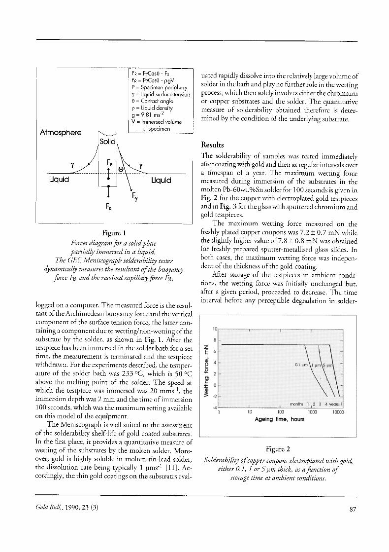
Figure 1Forces diagram for a solid platepartially immersed in a liquid.
The GEC Meniscograph solderability testerdynamically measures the resultant of the buoyancy
force FB and the resolved capillary force FR.
logged on a computer. The measured force is the resul-tant of the Archimedean buoyancy force and the verticalcomponent of the surface tension force, the latter con-taining a component due to wetting/non-wetting of thesubstrate by the solder, as shown in Fig. 1. After thetestpiece has been immersed in the solder bath for a settime, the measurement is terminated and the testpiecewithdrawn. For the experiments described, the temper-ature of the solder bath was 233 °C, which is 50 °Cabove the melting point of the solder. The speed atwhich the testpiece was immersed was 20 mms -1 , theimmersion depth was 2 mm and the time of immersion100 seconds, which was the maximum setting availableon this model of the equipment.
The Meniscograph is well suited to the assessmentof the solderability shelf-life of gold coated substrates.In the first place, it provides a quantitative measure ofwetting of the substrates by the molten solder. More-over, gold is highly soluble in molten tin-lead solder,the dissolution rate being typically I µms 1 [11]. Ac-cordingly, the thin gold coatings on the substrates eval-
uated rapidly dissolve into the relatively large volume ofsolder in the bath and play no further role in the wettingprocess, which then solely involves either the chromiumor copper substrates and the solder. The quantitativemeasure of solderability obtained therefore is deter-mined by the condition of the underlying substrate.
Results
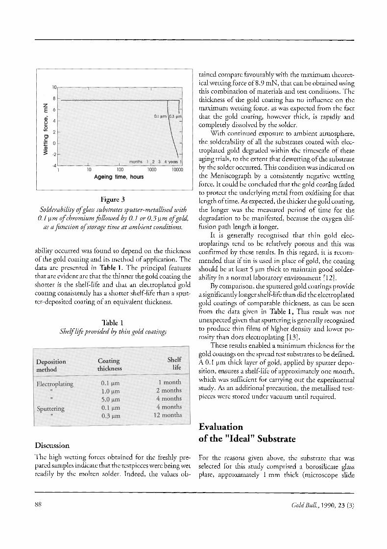
The solderability of samples was tested immediatelyafter coating with gold and then at regular intervals overa timespan of a year. The maximum wetting forcemeasured during immersion of the substrates in themolten Pb-60wt.%Sn solder for 100 seconds is given inFig. 2 for the copper with electroplated gold testpiecesand in Fig. 3 for the glass with sputtered chromium andgold testpieces.
The maximum wetting force measured on thefreshly plated copper coupons was 7.2 ± 0.7 mN whilethe slightly higher value of 7.8 ± 0.8 mN was obtainedfor freshly prepared sputter-metallised glass slides. Inboth cases, the maximum wetting force was indepen-dent of the thickness of the gold coating.
After storage of the testpieces in ambient condi-tions, the wetting force was initially unchanged but,after a given period, proceeded to decrease. The timeinterval before any perceptible degradation in solder-
Figure 2
Solderability of copper coupons electroplated with gold,either 0.1, 1 or 5 gm thick, as a function of
storage time at ambient conditions.
Gold Bull. : 1990, 23 (3) 87
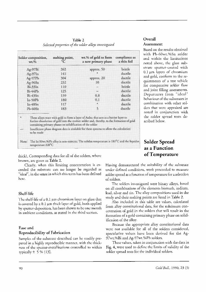
Figure 3
Solderability ofglass substrates sputter-metallised with0.1 µm of chromium followed by 0.1 or 0.3 µm ofgold,
as a function of storage time at ambient conditions.
ability occurred was found to depend on the thicknessof the gold coating and its method of application. Thedata are presented in Table 1. The principal featuresthat are evident are that the thinner the gold coating theshorter is the shelf-life and that an electroplated goldcoating consistently has a shorter shelf-life than a sput-ter-deposited coating of an equivalent thickness.
The high wetting forces obtained for the freshly pre-pared samples indicate that the testpieces were being wetreadily by the molten solder. Indeed, the values ob-
tamed compare favourably with the maximum theoret-ical wetting force of 8.9 mN, that can be obtained usingthis combination of materials and test conditions. Thethickness of the gold coating has no influence on themaximum wetting force, as was expected from the factthat the gold coating, however thick, is rapidly andcompletely dissolved by the solder.
With continued exposure to ambient atmosphere,the solderability of all the substrates coated with elec-troplated gold degraded within the timescale of theseaging trials, to the extent that dewetting of the substrateby the solder occurred. This condition was indicated onthe Meniscograph by a consistently negative wettingforce. It could be concluded that the gold coating failedto protect the underlying metal from oxidising for thatlength of time. As expected, the thicker the gold coating,the longer was the measured period of time for thedegradation to be manifested, because the oxygen dif-fusion path length is longer.
It is generally recognised that thin gold elec-troplatings tend to be relatively porous and this wasconfirmed by these results. In this regard, it is recom-mended that if tin is used in place of gold, the coatingshould be at least 5 µm thick to maintain good solder-ability in a normal laboratory environment [12].
By comparison, the sputtered gold coatings providea significantly longer shelf-life than did the electroplatedgold coatings of comparable thickness, as can be seenfrom the data given in Table 1. This result was notunexpected given that sputtering is generally recognisedto produce thin films of higher density and lower po-rosity than does electroplating [13].
These results enabled a minimum thickness for thegold coatings on the spread test substrates to be defined.A 0.1 µm thick layer of gold, applied by sputter depo-sition, ensures a shelf-life of approximately one month,which was sufficient for carrying out the experimentalstudy. As an additional precaution, the metallised test-pieces were stored under vacuum until required.
Evaluationof the "Ideal" Substrate
For the reasons given above, the substrate that wasselected for this study comprised a borosilicate glassplate, approximately 1 mm thick (microscope slide
88 Gold Bull.,1990, 23 (3)
manufactured to BS3836), that was degreased, sputteretched, and then sputter-metallised with a 0.1 µm layerof chromium, immediately followed by 0.1 µm of gold.To assess how closely the properties of this substratematched those of the "ideal" substrate defined above,the following evaluation was carried out, using thePb-60wt.%Sn solder.
WettabilityThe dynamic wetting behaviour of molten Pb-60wt.%Sn solder on the metallised glass substrates wasmeasured both in air, in the presence of a flux contain-ing 1 vol.% HCl as the active ingredient, and in vacuo,using the GEC Meniscograph wetting balance. In otherrespects, the experimental conditions were identical tothose used for the shelf-life assessment described above.
A maximum wetting force of 7.8 mN was recordedin vacuo a few seconds after immersing the testpiece intothe molten solder, as compared with a value of 8.7 mN,when the test was made in air using flux. The rapidattainment of a high and stable wetting force under bothconditions indicated that the substrate was being wetreadily by the molten solder. The maximum wettingforces measured can be compared with the maximumtheoretically attainable force of 8.9 mN. Using thisfigure, it was calculated that the measured wetting forcescorresponded to contact angles of 27° and 12°, for thetestpieces tested in vacuum and in air using flux, respec-tively. The poorer solder wetting of the substrate invacuo, without the aid of a flux, arises from the fact thata vacuum is incapable of reducing the oxide film thatwill be present on the surface of the molten solder.Indeed, virtually identical values of contact angle aremeasured if the test is made in air but with a "non-ac-tivated" (i.e. less aggressive) flux applied to the testpiece[14].
Extent of Solder/Substrate InteractionsIn the experiments of solder spread described below, thesolder foils used were 50 tm thick, which is typical ofthe solder foils used in the electronics industry. A 50 µmthick foil represents a reasonable compromise betweencost of the material, cost of fabrication and ease ofhandling. When a foil of this thickness is placed on a
substrate coated with a 0.1 tm thick gold metallisationand proceeds to totally dissolves it, the resulting con-centration of gold will be approximately 0.4 wt.%,assuming a typical solder density of 10 x 10 3 kgm 3 andthat the solder does not spread. This is well below thelevel at which the intermetallic compound AuSn4 willform as a primary phase in lead-tin solders and indeedin the other tin-based alloys used in this study [4].
As the solder spreads, the situation will be reachedwhere significant concentrations of gold are accumu-lated by the advancing solder front. By referring to theappropriate constitutional diagram, it is possible tocalculate the limit of spread for the solder alloy ofinterest at which the concentration of gold becomessufficient to form a gold-based intermetallic phase onsolidification. Gold concentrations below this level donot have a significant effect on the spread characteristicsof molten solders [15]. The limiting values, whereknown and relevant, have been marked on Fig. 4, whichdepicts the relationship between solder spread and goldconcentration, for a 1.4 mm 3 volume of solder (corre-sponding to a preform 6 mm in diameter and 50 µm
Figure 4Calculated concentration ofgold
as a function ofsolder spread ratio, assuming that the allof the 0.1 µm thick gold coating dissolvesand is uniformly distributed throughout
the volume of the molten solder.
Gold Bull., 1990, 23 (3) 89
Table 2Selected properties of the solder alloys investigated
Solder composition, melting point, wt.% of gold to form compliance as.wt.% °C a new primary phase a thin foil
These alloys react with gold to form a layer ofAuln2 that acts as a barrier layer tofurther dissolution of gold into the molten solder and, thereby, to the formation of goldcontaining primary phases on solidification of the solder
Insufficient phase diagram data is available for these systems to allow the calculation'to be made
OverallAssessmentBased on the results obtainedwith Pb-60wt.%Sn solderand within the limitationsnoted above, the glass sub-strate sputter-coated with0.1 µm layers of chromiumand gold, conform to the re-quirements of a test vehiclefor comparative solder flowand joint filling assessments.Departures from "ideal"behaviour of the substrates incombination with other sol-ders that were appraised arenoted in conjunction withthe solder spread tests de-scribed below.
Solder Spreadas a Functionof Temperature
Note: The In-50wt.%Pb alloy is non-eutectic. The solidus temperature is 180 °C and thetemperature 220 °C
thick). Corresponding data for all of the solders, whereknown, are given in Table 2.
Clearly, when this limiting concentration is ex-ceeded the substrate can no longer be regarded as"ideal", in the sense in which this term has been definedhere.
Shelf-lifeThe shelf-life of a 0.1 tm chromium layer on glass thatis covered by a 0.1 µm thick layer of gold, both appliedby sputter-deposition, has been shown to be one monthin ambient conditions, as stated in the third section.
Ease andReproducibility of FabricationSamples of the substrate described can be readily pre-pared in a highly reproducible manner, with the thick-ness of the sputter-metallisations controlled to withintypically± 5% [13].
Having demonstrated the suitability of the substrateunder defined conditions, work proceeded to measuresolder spread as a function of temperature for a selectionof solders.
The solders investigated were binary alloys, basedon all combinations of the elements bismuth, indium,lead, silver and tin. The alloy compositions used in thestudy and their melting points are listed in Table 2.
Also included in this table are values, calculatedfrom alloy constitutional data, for the minimum con-centration of gold in the solders that will result in theformation of a gold-containing primary phase on solid-ification of the alloy.
Because the appropriate alloy constitutional datawere not available for all of the solders considered,speculative values have been derived for the Ag-97wt. %Bi and Ag-97wt.%Pb solders.
These values, taken in conjunction with the data inFig. 4„ were used to define the limits of validity of thesolder spread tests for the individual solders.
90 Gold Bull., 1990, 23 (3)
ExperimentalProcedures
Small ingots of each of the solder alloys was prepared inthe manner described above. These were subsequentlycold-rolled to produce thin ductile foils approximately50 µm thick. The Ag-97wt. %Bi, Bi-33wt.%In and Bi
-43wt.%Sn solders proved too brittle to reduce to foilsby this method. Foils of these alloys were instead pro-duced by the chill-block melt-spinning technique. Thisprocess involves forcing a molten charge through a slotonto a rapidly spinning, water cooled, copper wheel.The high rate of heat extraction obtained by thismethod causes the molten alloy to solidify almost in-stantaneously on striking the wheel, resulting in theformation of a thin strip of the solder alloy with a finemicrostructure. By controlling the casting conditions,it is possible to produce the strip directly to the desiredthickness. The Bi-43wt.%Sn alloy is reasonably ductilewhen prepared in this manner.
Discs of the various solders, measuring 6 ± 0.1 mmdiameter, were stamped out of the foils and one discplaced centrally on glass substrates up to 25 mm x25 mm in area, that had been sputter-coated with thinchromium and gold layers. The testpieces were loadedinto a silica tube, which was evacuated to a pressure of1 x 10-4 Pa, and the entire assembly then inserted intoa furnace that had been preheated to the requisitetemperature. The temperature of the solder was moni-tored continuously during the heating cycle by a cali-brated thermocouple in contact with the centre of thesolder disc. The testpieces were maintained at the settemperature for one hour, after which the furnace waswithdrawn to produce rapid cooling to below the soli-dus temperature of the solder.
Following the heating cycle, the total area of thesubstrate over which the solder had spread was measuredusing an Optomax V Image Analysis System. The test-pieces were viewed on this instrument at a magnifica-tion of x5, giving an effective area resolution of300 µm2 , The spread measurement was normalised toa spread factor, being the ratio of the area of solderspread to the original area of the solder disc (28 mm 2).Thus, if a solder did not spread at all, the spread ratiois one, whereas if a solder flowed to cover an area of280 mm2, the spread ratio is ten. A spread ratio of 14was the test limit, defined by the area of the largestsubstrates.
15
13 "
O 11 - Sn Pb Sn-Ag Sn. in, Sn Bi`
ä 9
7
c% 5
3 ;
0 25 50 75 100 125 150
Excess temperature, ° C
Figure 5Spread characteristics of binary tin-based solder alloys
as a function of excess temperatureabove the melting point.
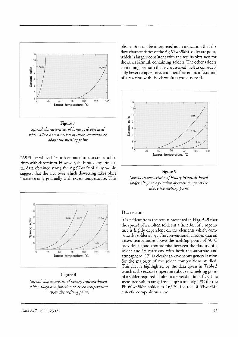
ResultsThe measured spread factors of eight common indus-trial solders on the notionally "ideal" substrate, arepresented in Figs. 5-9. To facilitate comparison of thedata, the scales used in these figures are the same andeach spread curve has been presented twice so that there
1s
13;
O 11 PbSn Pb-In
9
N 7 ''
c% 5
3 Pb-Bi
1 i0 25 50 75 100 125 150
Excess temperature, °C
Figure 6
Spread characteristics of binary lead-based solder alloysas a function of excess temperature
above the melting point.
Gold Bull., 1990, 23 (3) 91
Plate 2
A typical spread test sequence, showing solder spread increasing as a function of temperature.The solder in this case is Ag-97wt. %In.
The apparent contrast variation between the solidified solder pools is an artefact of the photography,arising from the high reflectivity of the gold-coated substrates.
exists a complete family of spread curves for each of thefive elements common to the solders investigated. Typ-ically five spread tests were used to determine eachcurve, as exemplified by the sequence for the Ag-97wt.%In solder illustrated in Plate 2.
In every case there is a trend towards increasedspread the higher the excess temperature above themelting point of the solder at which the test is con-ducted. The relationship between solder spread andexcess temperature is ex-ponential in character.By comparing the spreadcurves it is possible torank the constituent ele-ments in order of theirtendency to flow over thesubstrate, namely: tin >lead > silver > indium >bismuth. This order isalso maintained withineach family of solders, ascan be seen from Table 3,
It should be notedthat no experimentaldata was obtained for theIn-50wt,%Pb solderabove 300 °C nor for theAg-97wt.%Pb solder atany temperature. This is
because at test temperatures above 300 °C, significantvolatilisation of the lead occurred from these alloys, asascertained from analysis of the grey deposit that con-densed on the walls of the silica tube at the mouth ofthe furnace. This is to be expected given the high vapourpressure of lead at these temperatures, coupled with thelow background pressure in the vacuum furnace [16].The volatilisation could be suppressed by performingthe spread test in argon at atmospheric pressure. How-
ever, the presence of theatmosphere significantlyaltered the spread char-acteristics of the soldersand therefore this ap-proach was not pursued.
No data are pre-sented for the Ag-97wt.%Bi solder. This isbecause this solder partlydewets from the sub-strate due to reactionwith the chromium, sothat the substrate loses its"ideal" characteristics.The reaction arises fromthe fact that the Ag-97wt.%Bi solder meltsat 262 °C, which is closeto the temperature of
Table 3Excess temperature above the melting point
of each solder required to achieve a spread ratio of5
Element AElement B Tin Silver Indium Bismuth
Tin_ 1 9 54 92
Lead 1 — * 76 126'Silver 9 * — 122 +'
Indium 54 76 122 — 165
Bismuth 92 126 + 165 —
Lead volatilises at temperatures above 300 °C in vacuum..The melting point of Ag-97wt.%Pb at 304 °C is therefore tohigh to enable measurements of spread to be made in vacuum.
+ Bismuth dissolves chromium at temperatures above 265 °C.Accordingly, the molten solder then dewets from the exposed'glass substrate.
92Gold Bull., 1990, 23 (3)
15
13
O 11 ' Ag-Sn Ag In
}
9
7
vii 5
3
1,0 25 50 75 100 125 150
Excess temperature, 'C
Figure 7Spread characteristics of binary silver-based
solder alloys as a function of excess temperatureabove the melting point.
268 °C at which bismuth enters into eutectic equilib-rium with chromium. However, the limited experimen-tal data obtained using the Ag-97wt. %Bi alloy wouldsuggest that the area over which dewetting takes placeincreases only gradually with excess temperature. This
observation can be interpreted as an indication that theflow characteristics of the Ag-97wt. %Bi solder are poor,which is largely consistent with the results obtained forthe other bismuth containing solders. The other solderscontaining bismuth that were assessed melt at consider-ably lower temperatures and therefore no manifestationof a reaction with the chromium was observed.
15
13>
O 11 '' Bi Sn
9
4% 7 .;
Bi P6
uni5
3 ä1 io
0 25 50 75 100 125 150
Excess temperature, °C
Figure 9Spread characteristics of binary bismuth-basedsolder alloys as a function of excess temperature
above the melting point.
15 II
13
11 y. /in/PY Fg
a0 7
0 25 50 75 100 125 150
Excess temperature, 'C
Figure 8
Spread characteristics of binary indium-basedsolder alloys as a function of excess temperature
above the melting point.
Discussion
It is evident from the results presented in Figs. 5-9 thatthe spread of a molten solder as a function of tempera-ture is highly dependent on the elements which com-prise the solder alloy. The conventional wisdom that anexcess temperature above the melting point of 50°Cprovides a good compromise between the fluidity of asolder and its reactivity with both the substrate andatmosphere [17] is clearly an erroneous generalisationfor the majority of the solder compositions studied.This fact is highlighted by the data given in Table 3which is the excess temperature above the melting pointof a solder required to obtain a spread ratio of five. Themeasured values range from approximately 1 °C for thePb-60wt.%Sn solder to 165 °C for the Bi-33wt.%Ineutectic composition alloy.
Gold Bull., 1990, 23 (3) 93
Some elements are clearly more effective at promot-ing flow than others. In particular, solders containingtin all exhibit consistently high spread, whereas thosebased on bismuth do not spread to any significant extentat excess temperatures above the melting point of lessthan 100 °G. Detailed analysis of the results showedthat the ranking order in terms of spread at a given excesstemperature above the melting point is: tin > lead >silver > indium '> bismuth. This ranking sequence ismaintained irrespective of the second constituent of thesolder. However, it was not found possible to extract a.specific weighting factor for the individual elements inrespect of their promotion of spread.
One major reason for there being no direct quanti-tative relationship between the elemental compositionand spread of a solder is that not all of the solders aresimple binary eutectics between the pure elements..Indeed, of the common alloys for which spread data wasobtained, only the Bi-43wt.%Sn and Pb-60wt.%Snsolders fit this description. All of the other alloys involveeither one or two intermetallic compounds or arewholly non-eutectic, such as In--50wt.%Pb.
The importance of this consideration is well illus-trated by comparing the spread characteristics of theIn-48wt.%Sn solder with those of pure indium andpure tin. The relevant curves are shown in Fig. 10. Thespread characteristics of the In-48wtt.%Sn solder do nothe between those of indium and tin, as might be ex-
Figure 10
Spread characteristics of pug indium, tin andthe In-48wt. %Sn solder allay as a function
of the excess temperature above the melting point.
pected if a simple relationship applied between soldercomposition and spread. Instead the spread of the alloyis actually inferior to that of either of the two elements,which would seem to confound the accepted wisdorrtthat eutectic solders have high fluidity compared withtheir constituent elements.
It is indeed surprising that the ranking order ofspread promoted by the various elements is so consis-tent, given the very different manner in which thevarious solders react with the substrate. This point ishighlighted by contrasting the manner in which thePb-60wt.%Sn, In-5O vt.%Pb and.In-48 vt.%Sn soldersreact with gold coated substrates. The Pb-6Gwt.%5nalloy can dissolve up to 5 wt.% of gold before here isany significant change to its spread characteristics, whenmolten [4], whereas the dissolution of any gold into theIn-5Owt.%Pb solder results in the solder becomingpasty through the formation of precipitates of the inter-metallic compound AuIn2 [18]. The reaction of theIn-48wt.%Sn solder with gold is again very differentwith the establishment of an interfacial layer of AuIn2,between the molten solder and the gold coating [4].Once established this interfacial layer acts as an effectivebarrier between the indium and the gold because disso-lution of the gold then appears to cease [4] .
Despite such differences, the spread data, scatteredin the literature indicates that the ranking order of tin> lead > silver > indium > bismuth for solder spread is.generally observed. This applies not only to, binaryalloys but also to ternary and quaternary alloys, whetheror not the tests are performed in vacuo or in air usingmild fluxes, and for a variety of substrates includingcopper, tin and mild steel [ 19,24,21,22] . However, it isto be noted that when spread tests are perforated in airusing a highly activated flux, the ranking order is altered[20]. This feature clearly demonstrates the interferingeffect fluxes can have. Hence the importance o `avoidingfluxes when attempting to obtain. basic data on solderproperties.
Conclusions
Gold coatings have a vital role to play in promotingsoldering in the absence of fluxes. The chemical inert-ness and ease of deposition of gold as a high integritycoating have been exploited in devising a suitable sub-
94 Gold Bull., 1990, 23 (3)
strate for making a quantitative assessment of the spreadof different solders.
This substrate comprises 0.1 gm thick layers ofchromium and gold sequentially applied by sputter-de-position to a borosilicate glass substrate. A 0.1 µm layerof gold has been shown to protect the underlying metalfrom the atmosphere under ambient conditions andpreserving its solderability for up to one month. Thesubstrate is readily wetted by molten solders, does notsignificantly modify the metallurgical characteristics ofmost common solder alloys and is readily fabricated.
Departures from this "ideal" behaviour were onlyseen to occur at high spread ratios, where the pick-upof gold can become significant, and with one of thesolders evaluated, namelyAg-97wt. %Bi, that was foundto react with the chromium underlayer to cause dewett-ing. The spread of nine binary solders comprising com-binations of the elements bismuth, indium, lead, silverand tin, determined in vacuo, on the specified substratehave been compared and the following trends identi-fied:
• The spread of solders increases at an acceleratingrate as the excess temperature above the meltingpoint of the solder increases.
Some of the solders spread more readily than oth-ers. A consistent ranking order of elements in termsof solder spread has been established, viz. tin > lead> silver > indium > bismuth. This pattern is con-sistent with the data scattered in the literature andis also applicable to other substrates. ❑
ABSTRACT
Solder spread is commonly used as a yardstick forassessing the quality of a soldered joint. However, thespread of a molten alloy is a function not only of thetemperature and cleanliness of the joint surfaces, butalso of the solder composition.
The beneficial properties of gold have been used todevise a test substrate for quantitatively measuring theintrinsic spread characteristics of nine solders compris-ing binary combinations of bismuth, indium, lead,silver and tin. The measurements were carried out invacuum without fluxes, to avoid extraneous effects. It
was ascertained that the constituents promote solderspread in a ranking order:
tin > lead > silver > indium > bismuth
This finding is consistent with other published data.
ACKNOWLEDGEMENTS
The assistance of Miss L. Lanier, of Universite desSciences et Techniques de Lille-Flandres-Artois, is grate-fully acknowledged in obtaining the data presented inFigs. 2 and 3.
The World Gold Council and The General ElectricCompany plc are acknowledged for their support of thisstudy.
REFERENCES
1 G.L. Bailey and H.C. Watkins, The flow of liquidmetals on solid metal surfaces and its relationship tosoldering, brazing and hot-dip coating; J. Inst.Met., 1951, 80, 57-76
2 K.S. Raman, A.A. Krishnan and W. Rama-chandra , The spreading characteristics of tin-leadsolders on copper, Ind. J. Tech., 1963, 1, 471
3 C.J. Thwaites, `The attainment of reliability inmodern soldering techniques for electronicassemblies; Int. Met. Rev., 1972, 17(9), 149-174
4 D.M. Jacobson and G Humpston, `Gold coatingsfor fuxless soldering, Gold Bull., 1989, 22, 9-18
5 R. Duckett and M.L. Ackroyd, `The influence ofsolder composition on the embrittlement ofsoft-soldered gold coatings'. Electroplat. Met. Finish.,1976, 29(5), 13-20
6 D.S. Evans and A. Prince, `The effect ofgold on thePb-1.5%Ag-1 %Sn solder; Mat. Res. Bull., 1982,17, 681-687
7 F.G_ Yost, 'Soldering to gold films Gold Bull.,1977, 10, 2-7
Gold Bull., 1990, 23 (3) 95
8 L.J. Rickabaugh, The effect of thin film depositionangle and substrate surface roughness on film dissolu-tion in molten 60Sn-40Pb solder, Electrocompon-ent Science and Technology, 1977, 4, 43-46
9 R.H. Minetti and L.J. Rickabaugh, 'Solderdissolution rates of evaporated and sputteredTi-Pd-Au and NiCr-Au thin films, Proc. 27thElectronic components Conf., Arlington,Virginia, 16-17 May, 1977, 212-219
10 D.M. Jacobson and I. Gunter, `The MeniscographSolderability Tester: Adaptation to VacuumSoldering', GEC Review, 1990, 6(2), in press
11 W.G. Bader, `Dissolution ofAu, Ag, Pt, Cu and Niin a molten tin-lead solder' Weldingj Res. Suppl.,1969, 48, 551S-557S
12 C.A. Mackay, Surface finishes and theirsolderability 'International Tin Research Institute,Publication No 561, 1979
13 N.S. Platakis and L. Missei, `Wet and VacuumCoating Processes, 'Metal Finishing, 1978, 76 (5),93-97; ibid. (6), 65-69; ibid. (7), 50-54; ibid. (8),56-61; ibid. (9), 65-68
14 A.J, Mayhew and G.R. Wicks, 'Solderability andcontact angle', Proc. Int. electronic packaging and
production con£, Brighton, England, 19-21 Oc-tober, 1971
15 R.N. Wild, Effects ofgold on the properties ofsolders'. IBM Federal Systems Div., Owego, Rep.No. 67-825-2157, January 1968
17 H.H. Manko, 'Solders and soldering; (2nd ed.),New York, 1979, 56
18 M.M. Karnowsky and F.G. Yost, `The Au-In-Pbsystem: The AuIn2-In-Pb portion; Met. Trans.,1976,7A, 1149-1156
19 C.F. Knight and K.T. Harrison, Development ofzinc based solders' Proc. 4th British Associationfor Brazing and Soldering conf., London, 1-3 No-vember, 1983
20 R.N. Wild, `Properties ofsome low melting pointfusible solder alloys ; IBM Federal Systems Div.,Owego, Rep. No. 71Z000408, October 1971
21 D.H. Brewer, Solders for thick gold plating;Welding J. Res. Suppl., 1970, 49, 465-470
22 W.A. Mulholland and D.L. Willyard, 'Solderingto thin film hybrid microcircuits; Weldingi. Res.Suppl., 1974, 53, 466-474