38
Lead-free packaging for semiconductor devices E4 presentation Infineon Technologies / ST Microelectronics / Philips Semiconductors / Freescale Semiconductor 24 March 2005

Lead-free packaging for semiconductor devices
E4 presentationInfineon Technologies / ST Microelectronics / Philips Semiconductors /Freescale Semiconductor
24 March 2005
Content
1 Aim of this document2 Legislation3 Target / Status4 Standardisation5 Moisture Sensitivity Level (MSL) statements6 Technology7 Compatibility = Processability, Solderability, Reliability8 Conversion Roadmap9 Conclusion
Appendix: whisker
Aim of document
Information exchange
• Inform about ST / Philips SC / IFX / Freescale (E4) activities on lead-free packaging
• Collect feedback regarding preferred approach and roadmap

Effect of EU Directive
• On 13th of February 2003, directive 2002/95/EC of the European Parliament and of the Council of 27th January 2003 on the Restriction of the use of certain Hazardous Substances in electrical and electronic equipment (RoHS) entered into force. The directive will be applicable throughout EU by 1st July 2006 for the ban on the use of certain substances including lead (Pb)
• Considering that semiconductor devices as well as finished electronics can be stored before usage or selling, conversion tolead-free should take place with suitable advance on the 1st July 2006 deadline
Legislation
• The E4 classifies a product as “green” when it is compliant to RoHS: free*from the substances Pb, Hg, Cd, Cr6+,PBB and PBDE
* Max. concentration limits to be respected.
• The actual packages do NOT contain Hg,Cd,Cr6+,PBB and PBDE!Therefore the elimination of Pb will result in the package classification “green”.
It may be remarked that the presence of exempted Pb does not affect the classification “green” (e.g. Pb based die-attach alloys).
• Part of the packages is halogen free. The industrial availability of this type of materials is still limited and full implementation might take some years.
RoHS compliance, green package

Target / Status
Pb-free Programs in the Industry
Two Targets:• Compatibility with both SnPb and Pb-free board soldering
(with extended temperature range)• Elimination of Pb in package terminals (leads, balls, bumps)
Status• Main Japanese consumer market converted to lead-free soldering• Major conversion to lead free components by 1H05

StandardisationIPC/JEDEC J-STD-020C
• IPC/JEDEC published an updated spec per July 2004 : J-Std-020C • Main changes compared to J-Std-020B :
– 9 categories (3x thickness, 3x volume ) in stead of 4 today :
– 245°C, 250°C and 260°C as specified package peak temperatures.
• The E4 comply to the new conditions with following notes :– The more tough conditions will impact the MSL for a substantial
part of the products; restore of the MSL will need engineering time and effort and will also depend on the availability of new materials.
Package Thickness Volume < 350 mm3 Volume 350 - 2000 mm3 Volume > 2000 mm3
<1.6 mm 260 260 2601.6 mm - 2.5 mm 260 250 245
> 2.5 mm 250 245 245

StandardisationE4-profile vs. J-STD 020C - designed for lead-free MSL evaluation
e.g. @ 260°C for small packages
Time in s
t 25 °C to Peak
100
200
20406080
120140160180
220240260
30 60 12090 150 180 210 240 270 300 330 360 390
Tem
pera
ture
in °
C
Tsmin Tsmax
TL
tp
Ramp-up
Critical ZoneTL to tp
Ramp-down
TP
tL

MSL statements
• Hundreds of packages in the 4 companies have been tested according to the agreed profiles, following JEDEC STD-020C for the pre-conditioning process and for failure criteria.
• With present materials and package design, in specific cases a degradation of MSL classification may be observed
Lower MSL as temporary action,qualification of new materials (ongoing) as short/mid term action
Source Infineon
Technology
Consolidated lead free solutions:
For lead frame based packages • Post plate of matte tin • Pre plate of NiPdAu
For Ball Grid Array packages • SnAgCu
Note: technology may differ per package family / company

TechnologyPostplate of matte tin (Sn)
Main characteristics
• Material availability is good• Closest to SnPb in cost and process• Good solderability with SnPb and Pb free solders• Good solder joint reliability• Good compatibility with SnPb Solder • “Whisker free” process available 1)
1) See whisker presentation
TechnologyPreplate NiPdAu*
Main characteristics
• Good solderability with SnPb and Pb free solders• Good solder joint reliability• Used in high volume • Offered by major lead frame suppliers
* NiPdAu lead finish is a selective alternative for some packages.
TechnologySnAgCu Spheres in Ball Grid Array
Main characteristics
• SnAg3.0-4.0Cu0.5-1.0 is the most applied range • Good solderability with Pb free solders• Offered by all major suppliers• Limited backward compatibility with SnPb solders
(board application process to be adopted)

Today
Experience of some
decades of board assembly
Increase temp. by 20°C
supplier
customerPb – solder (215-240C) Pb – solder (235-260C)
Pb
Pb
com
pone
nt fi
nish
Lead-Frame packages Compatibility
(NCMS-, IDEALS-report,internal evaluations)
Processability: o.k.
Solderability: o.k.
Reliability: o.k.
Processability: o.k.
Solderability: o.k.
Reliability: o.k.
Processability: o.k.
Solderability: o.k.
Reliability: o.k.

Only slight differences of wetting ( ) , fillet ( )Surface: less shiny for lead-free (see inserts)
Lead-Frame Packages ProcessabilityReflow solder joints
Lead containing solder Lead-free solderBackward Compatibility SC, reduced dT
SnAg3.8Cu0.7
0
50
100
150
200
250
300
0 60 120 180 240 300 360 420
Time in seconds
Tem
pera
ture
in d
egre
e C
FQFP208HVQFN48VSO56HTQFP100SO28
260
235
Backward Compatibility SCSnPb36Ag2
0
50
100
150
200
250
300
0 100 200 300 400
Time in seconds
Tem
pera
ture
in d
egre
e C
FQFP208HVQFN48VSO56HTQFP100SO28
260
205
Source Philips

Lead-Frame Packages ProcessabilityWave solder joints
Lead containing solder Lead-free solder
Only difference:somewhat less shiny with lead-free
Process Process speed
[m/min]
Total soldering time/temp
Pre-heat temperature
Leaded 1.25 2.75±0.25s / 250°C 120±10°CLead-free 1.2 3.75±0.25s / 265°C 120±10°C Source Philips

Lead-Frame Packages ProcessabilityProcessability in lead containing vs. lead-free process
• For reflow soldering: paste application, component placement do not require special measures
• For wave soldering: glue application, component placement, glue cure do not require special measures
• Differences in soldering process are time and temperature
• SnPb plating and Sn plating do not show a different behavior in the soldering processes (more than a decade of experience!)
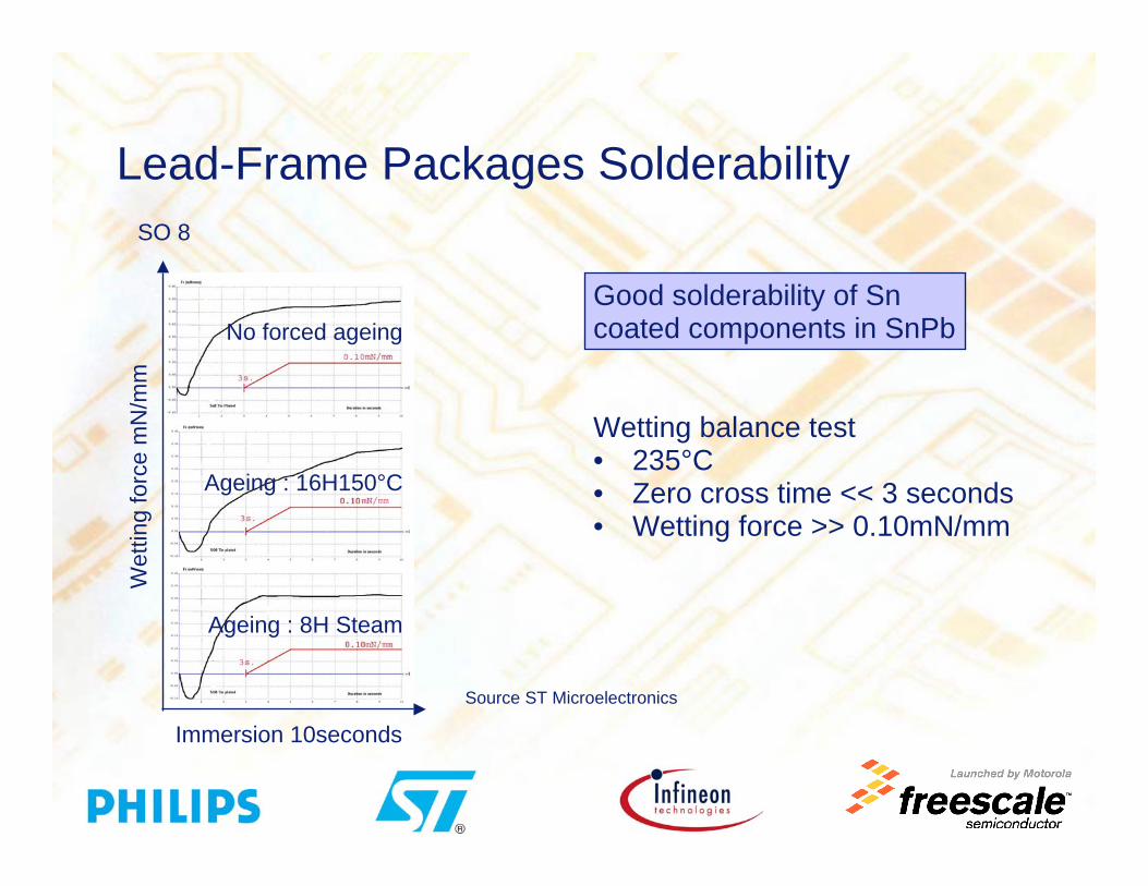
Lead-Frame Packages Solderability
Good solderability of Sncoated components in SnPb
Wetting balance test• 235°C• Zero cross time << 3 seconds• Wetting force >> 0.10mN/mm
Immersion 10seconds
SO 8
Wet
ting
forc
e m
N/m
m
Ageing : 16H150°C
No forced ageing
Ageing : 8H Steam
Source ST Microelectronics
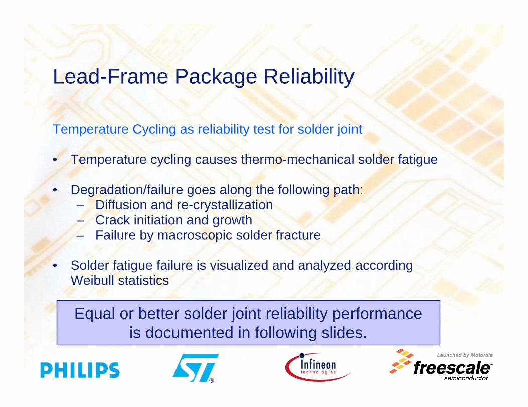
Lead-Frame Package Reliability
Temperature Cycling as reliability test for solder joint
• Temperature cycling causes thermo-mechanical solder fatigue
• Degradation/failure goes along the following path:– Diffusion and re-crystallization– Crack initiation and growth– Failure by macroscopic solder fracture
• Solder fatigue failure is visualized and analyzed according Weibull statistics
Equal or better solder joint reliability performanceis documented in following slides.

Source PhilipsN cycles
HTQFP100, reflow
0,01
0,1
1
10
100 1000 10000
N cycles
ln[1
/(1-f)
]
SnPbSnAgCu
Lead-Frame Package Reliability
Weibull analysis of failure in temperature cycle test(-40/+125 oC) Pb-free and Pb-containing reflow solderSn plated HTQFP100 components (Cu-based lead-frame)

LQFP208, reflow
0,01
0,1
1
10
100 1000 10000
N cycles
ln[1
/(1-f)
]
SnPbSnAgCu
Source Philips
Lead-Frame packages Reliability
Weibull analysis of failure in temperature cycle test (-40/+125 oC) Pb-free and Pb-containing reflow solderSn plated LQFP208 components (Cu-based leadframe)

VSO56, reflow
0,01
0,1
1
10
100 1000 10000
N cycles
ln[1
/(1-f)
]
SnPbSnAgCu
Source Philips
Lead-Frame packages Reliability
Weibull analysis of failure in temperature cycle test (-40/125 oC) Pb-free and Pb-containing reflow solderSn plated VSO56 (FeNi42-leadframe)

Both combinations, Sn finish with SnPb solder and Sn finish with SnAgCu solder, perform equal to or better than SnPb finish with SnPb solder.
Board assembly with SnPb solder paste was performed at the standard SnPb profile.
Sn-SnPb2
SnPb-SnPb1
SnPb-SnAgCu3
Finish-Solder
1) Current, 220°C reflow
2) Backwards compatible, 220°C reflow
3) Forwards compatible, 240°C reflow
4) Pb-free, 240°C reflow
Number of Temperature Cycles
--50°C/150°C50°C/150°C
%
Packages
Failed
Sn-SnAgCu4
Lead-frame packages Reliability132 PQFP Board-Level Air-Air Temperature Cycling
Source Freescale

Lead-Frame Packages Reliability
Source Freescale
Weibull analysis of failure in temperature cycle test (-40/+125C) comparing Pb-free and Pb-containing reflow solder
Sn-SnAgCu4
has no fails as of 13407 cycles,
dashed line represents worse case estimation.
Sn-SnAgCu4
has no fails as of 13407 cycles,
dashed line represents worse case estimation.
64LQFP Board-Level Air-Air Temperature Cycling
Number of Temperature Cycles
%
Packages
Failed
Both combinations, Sn finish with SnPb solder and Sn f in ish wi th S n A g C u s o l d e r , perform equal to or better than SnPb finish w i t h SnPb so lder .
Board assembly with SnPb solder paste was p e r f o r m e d a t t h e standard SnPb profile.
Sn-SnPb2SnPb-SnPb1
SnPb-SnAgCu3
Finish-Solder
1) Current, 220°C reflow
2) Backwards compatible, 220°C reflow
3) Forwards compatible, 240°C reflow
4) Pb-free, 240°C reflow
Sn-SnAgCu4

Lead-Frame packages Reliability
Reliability result for solder joint reliability with Pb-free components metallization by the ‘Fraunhofer Institute’ (-40C/125C)
Number of Thermal Cycles1000 2000 3000 4000 5000
%
Cum
ulat
ive
Fai
lure
s
0.2
0.4
1
2
4
10
2030
5070
99.9
2984
,65
Failure statistics for P-TQFP-100-1Sn-plating SnAgCu-paste on AuNi
NiFe-leadframe
P-TQFP-100-1 on Au/Ni (SnAg3.8Cu0.7-after4000 Cycles)
SnPb36Ag2 SnAg3.8Cu0.7
Cu/OSP Au/Ni Cu/OSP Au/Ni
CumulatedFailures
(4000 Cycles)
CharacteristicLifetime
(cycles)
CumulatedFailures
(4000 Cycles)
CharacteristicLifetime
(cycles)
CumulatedFailures
(4000 Cycles)
CharacteristicLifetime
(cycles)
CumulatedFailures
(4000 Cycles)
CharacteristicLifetime
(cycles)
P-DSO-12-2 (11) n.e. (10) n.e. (6) n.e. (2) n.e.
P-VQFN-48-4 8 5233 12 4134 17 3704 17 3891
P-TQFP-100-1 24 2281 24 2480 24 2208 24 2985
P-TQFP-100-5 0 n.e. 2 n.e. 0 n.e. 0 n.e.
Source: Infineon - IZM report UB.412.DL.2003.01(x) = package internal contact failure

MINIMUM REQUIREMENTS for Product Qualification Matte tin (Sn), Whisker related tests
1. High temp. / high humidity55-60°C / 85% rel. Hum. 2* 1000h max. 50µm whisker 1*
2. Temperature cycle-40°C / +85°C 1000TC max. 50µm whisker
3. AmbientUncontrolled ambient 8 weeks max. 20µm whisker
1* whisker length is measured by adding sub-sections. Density or distribution are not relevant.2* if corrosion occurs test is to be repeated
Positive results on above test will lead to a release of the Sn-plating technology regarding whisker issue.
The E4 Product Qualification criteria were established to meet the specifications of a majority of customers requiring Pb-free product shipments today. They will be used until relevant Standard is released. Members actively contribute to the ongoing definition of these Standards by performing extended tests beyond the targets indicated above.
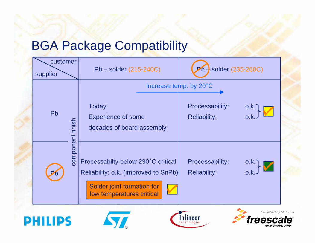
Today
Experience of some
decades of board assembly
Increase temp. by 20°C
supplier
customerPb – solder (215-240C) Pb – solder (235-260C)
Pb
Pb
com
pone
nt fi
nish
Processability: o.k.
Reliability: o.k.
Processability: o.k.
Reliability: o.k.
Processabilty below 230°C critical
Reliability: o.k. (improved to SnPb)
BGA Package Compatibility
Solder joint formation forlow temperatures critical

BGA Processability
Motivation:For array-package the processability hasbeen tested. Different temperature at theball result in different mounting height.
Conclusion:The combination Pb-free BGA/SnPb-pastecan be processed with a minimumtemperature of 230°C (at the ball). Due to limited self-alignment, a solderjoint temperature at 220°C should only be chosen in exceptional cases
Solder joint temperatures over 230°C are recommended
mountingheight
bad joint good solder jointwith limited drop
good solder joint
Beginning melting
Complete melting, final height
decreasing mounting height
Source Infineon

BGA On Board Reliability
Pb-free solder balls shear test
Pb-free solder balls are showing same initial shear strength thanSnPb balls but shear values remains more stable during ageing
Source ST Microelectronics
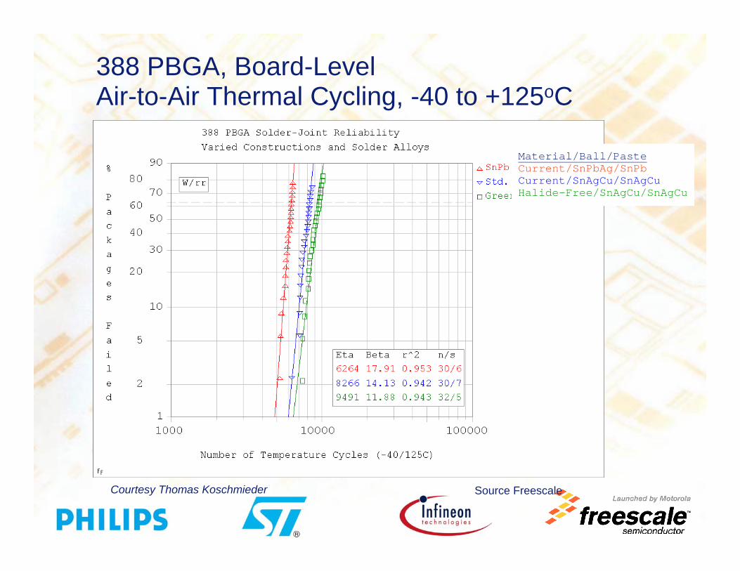
388 PBGA, Board-Level Air-to-Air Thermal Cycling, -40 to +125oC
Courtesy Thomas Koschmieder
Material/Ball/PasteCurrent/SnPbAg/SnPbCurrent/SnAgCu/SnAgCuHalide-Free/SnAgCu/SnAgCu
Source Freescale
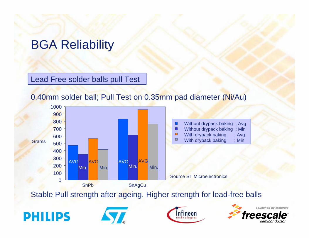
Lead Free solder balls pull Test
0.40mm solder ball; Pull Test on 0.35mm pad diameter (Ni/Au)
Stable Pull strength after ageing. Higher strength for lead-free balls
BGA Reliability
Source ST Microelectronics
SnPb SnAgCu
Min.AVG
Min.AVG
Min.AVG
Grams
Min.AVG
0100200300400500600700800900
1000
Without drypack baking ; AvgWithout drypack baking ; MinWith drypack baking ; AvgWith drypack baking ; Min

LFBGA-208, Ball SnAgCu, solder SnPbAg-40°C/+125°C, 2000 cycles
Results positive
BGA On board Reliability
Source Infineon
Further reference: for large BGA’s (35x35mm) positive results shown by: “Thermal Fatigue Resistance of Pb-free Second Level Interconnect”; Patrick Roubaud; SMTA 2001

BGA On board Reliability
Weibull analysis of failure in temperature cycle test lead-free and lead-containing reflow solder TFBGA6x6-46 with 0.4mm solder balls(both SnPb-SnAgCu)
Source ST Microelectronics
4 tested processes
SnPb balls + SnPb paste (220C)SnAgCu balls + SnPb paste (220C)
SnAgCu balls +SnAgCu paste (245C)SnAgCu balls +SnAgCu paste (250C)
-40°C/+125°C cycles

CompatibilityConclusion for compatibility
Leadframe-package• Processability: Sn plated products show identical behaviour as
SnPb plated products• Solderability: Sn- and NiPdAu surfaces are solderable with SnPb
and Pb-free solder paste• Solder joint reliability tested at >> 2000 TC does show no failure
BGA-package• Processability: good processabilty for temperature over 230°C • Solder joint reliability is improved compared to SnPb-balls
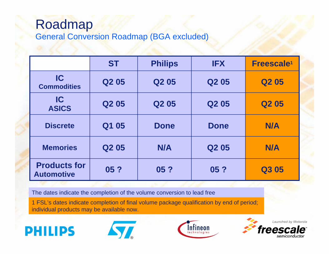
Roadmap General Conversion Roadmap (BGA excluded)
Q3 0505 ?05 ?05 ?Products forAutomotive
N/AQ2 05N/AQ2 05Memories
N/ADoneDoneQ1 05Discrete
Q2 05Q2 05Q2 05Q2 05ICASICS
Q2 05Q2 05Q2 05Q2 05ICCommodities
Freescale1IFXPhilipsST
The dates indicate the completion of the volume conversion to lead free
1 FSL’s dates indicate completion of final volume package qualification by end of period; individual products may be available now.

Roadmap IC Package Conversion Roadmap
Q2 05Q2 05doneQ2 05PLCC
Q1 05=Q2 05Q1 05SSOP
Q1 05doneQ2 05Q2 05 TSSOP
doneQ4 05Q2 05Q1 05SO
Q2 05donedonedoneQFN
Q3 05Q2 05done Q1 05M/L/T/QFP
Q1 05Q2 05Q3 05Q2 05 L/T/F BGAFreescale1IFXPhilipsST
The dates indicate the completion of the volume conversion to lead free
1 FSL’s dates indicate completion of final volume package qualification by end of period; individual products may be available now.
Conclusion
Leadframe packages• Sn-plating or NiPdAu-plating is introduced as lead-free technologies• For leadframe packages there is a full compatibility to SnPb- and
Pb-free solder process
BGA packages• For BGA packages SnAgCu is the chosen metallurgy• On board reliability is proven• In the case of BGA-packages the soldering temperature must be
above 230°C for processability
Note: technology may differ per package family / company

Thank you


