KYOTO ELEX CO., LTD 4th Metallization Workshop in Constance on 7-8 May,2013 [7]
Wafer
Isc
[A]
Jsc
[mA/cm2]
Voc
[V]
FF
η
[%]
Ag Wet
[g/cell]
8.460 34.77 0.631 0.802 17.58 0.093
8.454 34.74 0.628 0.803 17.51 0.090
8.524 35.03 0.628 0.797 17.54 0.095
8.858 37.22 0.633 0.796 18.73 0.107
8.846 37.17 0.632 0.803 18.88 0.095
8.837 37.13 0.633 0.803 18.85 0.094
Ave.
Wafer
Isc
[A]
Jsc
[mA/cm2]
Voc
[V]
FF
η
[%]
Ag Wet
[g/cell]
mc-Si 8.479 34.84 0.629 0.801 17.54 0.093
CZ-Si 8.847 37.17 0.632 0.801 18.82 0.099
mc-Si
CZ-Si
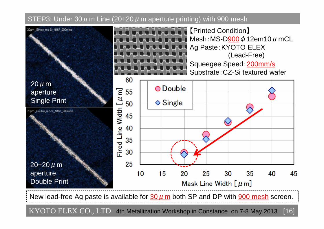
STEP1: Under 50μm Line (40+40μm aperture printing) with 500 mesh
KYOTO ELEX CO., LTD 4th Metallization Workshop in Constance on 7-8 May,2013 [8]
Comparison of Conventional Screen Printing with Our ChallengesConventional screen printing on solar cell
Our Challenges
Screen
Paste
Problem
Screen
Paste
Aims
①Screen life of high open area rate (60%) is short. ②Printing resolutions of high open area rate (60%) is bad.③High viscosity paste can’t print with high-mesh(=low open area rate)④So, we can’t print under 50 μm line in mss-production condition.
Higher open area rate (60%) delivers better paste release.
High viscosity paste has high silver content and gives good aspect rate.
①Achievement of minimum cross-section for high FF by double printing②Improvement of printing resolutions and optimization of under 50 μm printing
①3 times strength of standard stainless wires②40% open area rate③Ultra-fine mesh (#500/#650/#900) for target finger line width
Low viscosity and various control for screen of 40% open area rate and ultra-fine mesh to print under 50μm finger line
SEM Image of Mesh ①
KYOTO ELEX CO., LTD 4th Metallization Workshop in Constance on 7-8 May,2013 [9]
KYOTO ELEX CO., LTD 4th Metallization Workshop in Constance on 7-8 May,2013 [17]
Test Result High FF for high sheet resistance emitter
【Printed Condition】
Ag Paste:KYOTO ELEX(Lead-Free Ag Paste)Screen:
HS-D650Φ14em15μmCL(Ultra high mesh)Pattern:30+30μm150finger3busbar(Double Printing)
Emitter sheet resistance60⇒120Ω/□
・Keep high FF(≒0.800)・Increase Jsc
Pb
Conclusion
KYOTO ELEX CO., LTD 4th Metallization Workshop in Constance on 7-8 May,2013 [18]
・We’ve been able to achieve under 50μm line screen printing on solar cell wafer with properly tuned combination of ultra-High meshand new lead-free Ag paste.
・Every target line width from mass-production to next-generation, there are 3 steps which we propose the idea of screen specand they gives good fine line printing.
・In addition to ultra fine line, the new lead-free Ag paste suggests potential to be capable of adapting to over 100Ω/□ high sheet resistance cells (~120Ω/□).
・As of today, we get a part of the solutions toward 30μm line screen printing and 120Ω/□ cell available to get high performance solar cells. The end goal requires “ total optimizationof solar cell process”, not only individual improvement.