33
Out Common Source(CS) C Transfer Characterstics Configuration 2/12/2015 tline Configuration s in Common Source(CS) 1
| Date post: | 06-Dec-2015 |
| Category: |
Documents |
| Upload: | amandeep-gupta |
| View: | 213 times |
| Download: | 0 times |

Outline
Common Source(CS) Configuration
Transfer Characterstics in Common Source(CS) Configuration
2/12/2015
Outline
Common Source(CS) Configuration
Transfer Characterstics in Common Source(CS)
1

• Body Effect
CMOS
2/12/2015
Recap
2
Recap

Chapter 4 MOS field-Effect Transistors (MOSFETs)
Figure 4.9CMOS TransistorEffect Transistors (MOSFETs)
Figure 4.9Transistor

Common Source Amplifier
Biasing to be doneTo work at appropriate VGS
and corresponding ID
Common Source Amplifier
Two port Network

Common Source AmplifierCommon Source Amplifier
V0 = VDD- iDRD
Transconductance Amplifier
Converted to Voltage Amplifier

I-V Characterstics of common Source amplifer
2/12/2015
CB
Q
iD
of common Source amplifer
Q vGS= vIQ
vDS = vo
A

2/12/2015
I-V Characterstics of common Source amplifer
7
of common Source amplifer

I-V Characterstics of common Source amplifer
2/12/2015
CB
Q
iD
of common Source amplifer
Q vGS= vIQ
vDS = vo
A
Load Line
Slope of Load Line ?

2/12/2015
Y = m x + C Equation of straight line
I-V Characterstics of common Source amplifer
x + C Equation of straight line
Slope of Load line
of common Source amplifer

2/12/2015
CB
Q
iD
I-V Characterstics of common Source amplifer
vGS= vIQ
vDS = vo
A
of common Source amplifer

Case I
Case II
Transfer CharactersticsSource
vGS = 0.6
vGS = 1.2V
11
Characterstics of common Source amplifer
vt = 0.7
vDD = 5V
RD = 1K

2/12/2015
I-V Characterstics of common Source
12
of common Source amplifer
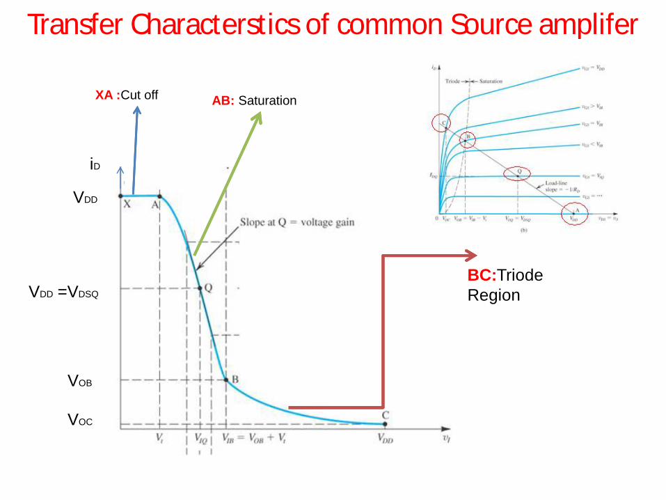
XA :Cut off AB: Saturation
VDD
VDD =VDSQ
VOB
VOC
Transfer Characterstics of common Source
iD
BC:Triode Region
of common Source amplifer

Digital Applications
Transfer Characterstics of common Source
14Digital Applications
of common Source amplifer

2/12/2015
I-V and Transfer
15
V and Transfer Characterstics

Operation as Switch
Digital Applications16
Operation as Switch
Digital Applications

Saturation
VDD =VDSQ
VOB
Operation as Linear AmplifierOperation as Linear Amplifier

Saturation
VDD =VDSQ
VOB
The positive peaks of the output signals might
VDSQ close to VDD ?
VDSQ close to Triode region ?
The positive peaks of the output signals might bump into VDD
close to VDD ?
close to Triode region ?

Chapter 4 MOS field-Effect Transistors (MOSFETs)
Figure E4.27Selection of Q pointEffect Transistors (MOSFETs)
Figure E4.27Selection of Q point
Slope of Load line based on RD

Cutoff Region
2/12/2015
Cutoff Region
20

Saturation Region
2/12/2015
Saturation Region
21

Saturation Region
2/12/2015
VDD =VDSQ
VOB
Saturation Region
22
Saturation

Saturation Region
2/12/2015
Saturation Region
23

Triode Region
2/12/2015
Triode Region
24

Triode Region
2/12/2015
Triode Region
25

Triode Region
2/12/2015
We know
Triode Region
26

Biasing by Fixing V
2/12/2015 EEE C424/ECE C313
Biasing by Fixing VGS
EEE C424/ECE C313 27
Selection of RD ?

Chapter 4 MOS field-Effect Transistors (MOSFETs)
Figure 4.30
FIGURE 4.30 Biasing using a fixed voltage at the gate, basic arrangement; (b) reduced variability in ID
Biasing by Fixing VGS and Connecting Resistance in the source
Effect Transistors (MOSFETs)
Figure 4.30
FIGURE 4.30 Biasing using a fixed voltage at the gate, VG, and a resistance in the source lead, RS: (a)
Biasing by Fixing VGS and Connecting Resistance in the source

FIGURE 4.30 (c) practical implementation using a single supply (e) practical implementation using two
Practical implementation using single and two supplies
FIGURE 4.30 (c) practical implementation using a single supply (e) practical implementation using two supplies.
Practical implementation using single and two supplies

FIGURE 4.30 (d) coupling of a signal source to the gate using a capacitor
Coupling of a Signal Source to the gate using a capacitor
FIGURE 4.30 (d) coupling of a signal source to the gate using a capacitor CC1
Coupling of a Signal Source to the gate using a capacitor CC1

Biasing MOSFET using large drain to gate feedback resistor R
Biasing MOSFET using large drain to gate feedback resistor RG

Biasing MOSFET using constant current source
Biasing MOSFET using constant current source

Implementation of constant current source using Current Mirror
Implementation of constant current source using Current Mirror


![Lec 8 03_sept [compatibility mode]](https://static.documents.pub/doc/80x56/558790e7d8b42a750b8b456e/lec-8-03sept-compatibility-mode.jpg)


