Lec. 8: Subranging/Two-step ADCs Lecturer: Hooman Farkhani Department of Electrical Engineering Islamic Azad University of Najafabad Feb. 2016. Email: [email protected]In The Name of Almighty
When the resolution is higher than 8-bit then instead of full-flash ADC, it can be
more convenient to use a sub-ranging or a two-step algorithm for a better speed-ac
curacy trade-off.
The sub-ranging or the two-step implementation require two (or three) clock pe
riods to complete the conversion but they use a smaller number of comparators thu
s benefitting silicon area, power consumption and parasitic capacitance loading on
the S&H.
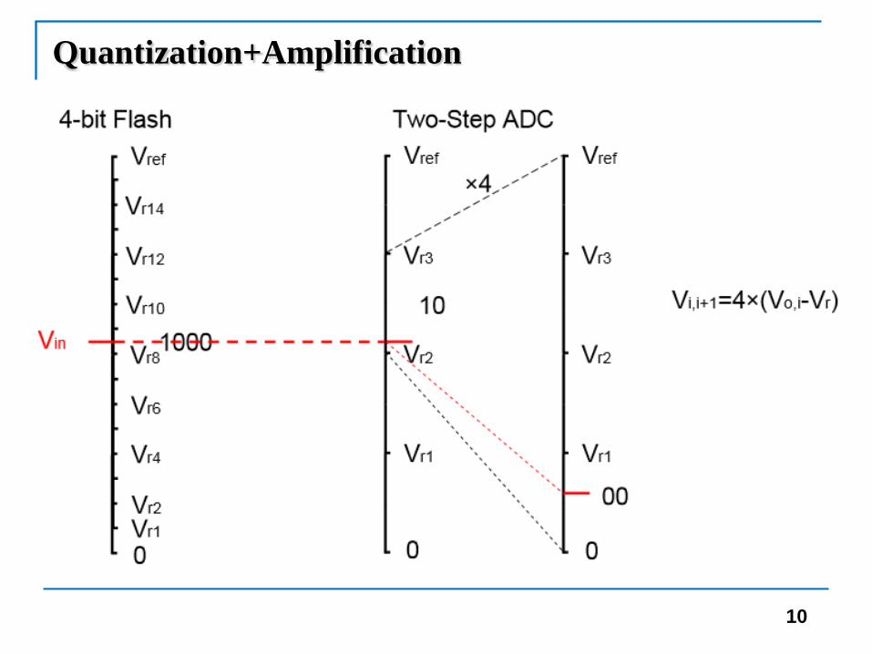
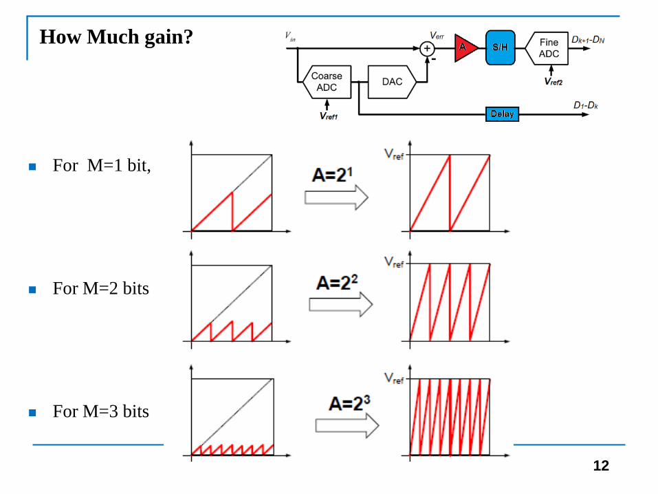
The architecture uses a sample-and-hold at the input to drive an M-bit flash-conve
rter which estimates the MSBs (coarse conversion). TheDAC then converts the M-bits back to an analog signal which is subtracted from the held input to give the co
arse quantization error (also called the residue). Next, the residue is converted into
digital by a second N-bits flash which yields the LSB (fine conversion). The digita
l logic combines coarse and fine results to obtain the n=(M+N)-bit output.
Sub-ranging: without gain (No amplification of residue)
Two-step: With amplifying the residue.
4
Sub-ranging/ Two-step
5
4-Bit Flash Vs. 4-Bit Two-Step ADC
6
Sub-ranging ADC
7
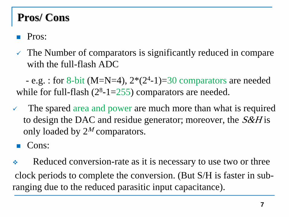
Pros/ Cons
Pros:
The Number of comparators is significantly reduced in compare
with the full-flash ADC
- e.g. : for 8-bit (M=N=4), 2*(24-1)=30 comparators are needed
while for full-flash (28-1=255) comparators are needed.
The spared area and power are much more than what is required
to design the DAC and residue generator; moreover, the S&H is
only loaded by 2M comparators.
Cons:
Reduced conversion-rate as it is necessary to use two or three
clock periods to complete the conversion. (But S/H is faster in sub-
ranging due to the reduced parasitic input capacitance).
8
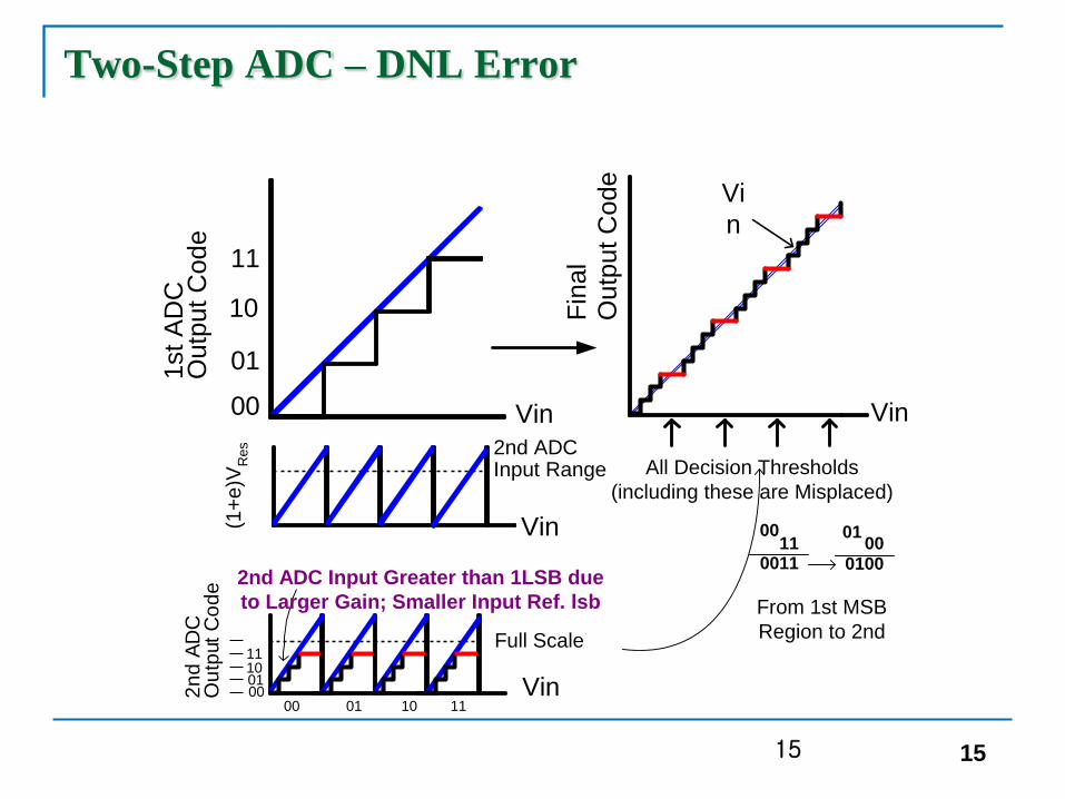
Delay of the Sub-ranging/Two-step ADC and possible Solution