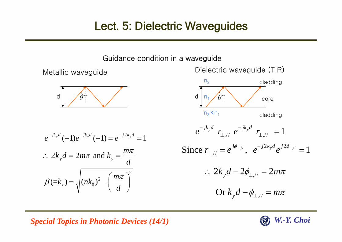
Lect. 5: Dielectric Waveguides Special Topics in Photonic Devices (14/1) W.-Y. Choi Guidance condition in a waveguide 2 2 2 0 ( 1) ( 1) 1 2 2 and (= ) ( ) y y y jk d jk d j kd y y z e e e m kd m k d m k nk d d Metallic waveguide ,// ,// 1 y y jk d jk d e r e r n 2 cladding d n 1 n 2 <n 1 core cladding Dielectric waveguide (TIR) ,// ,// Since , j r e ,// 2 2 2 y kd m ,// 2 2 1 y j kd j e e ,// Or y kd m
Transcript
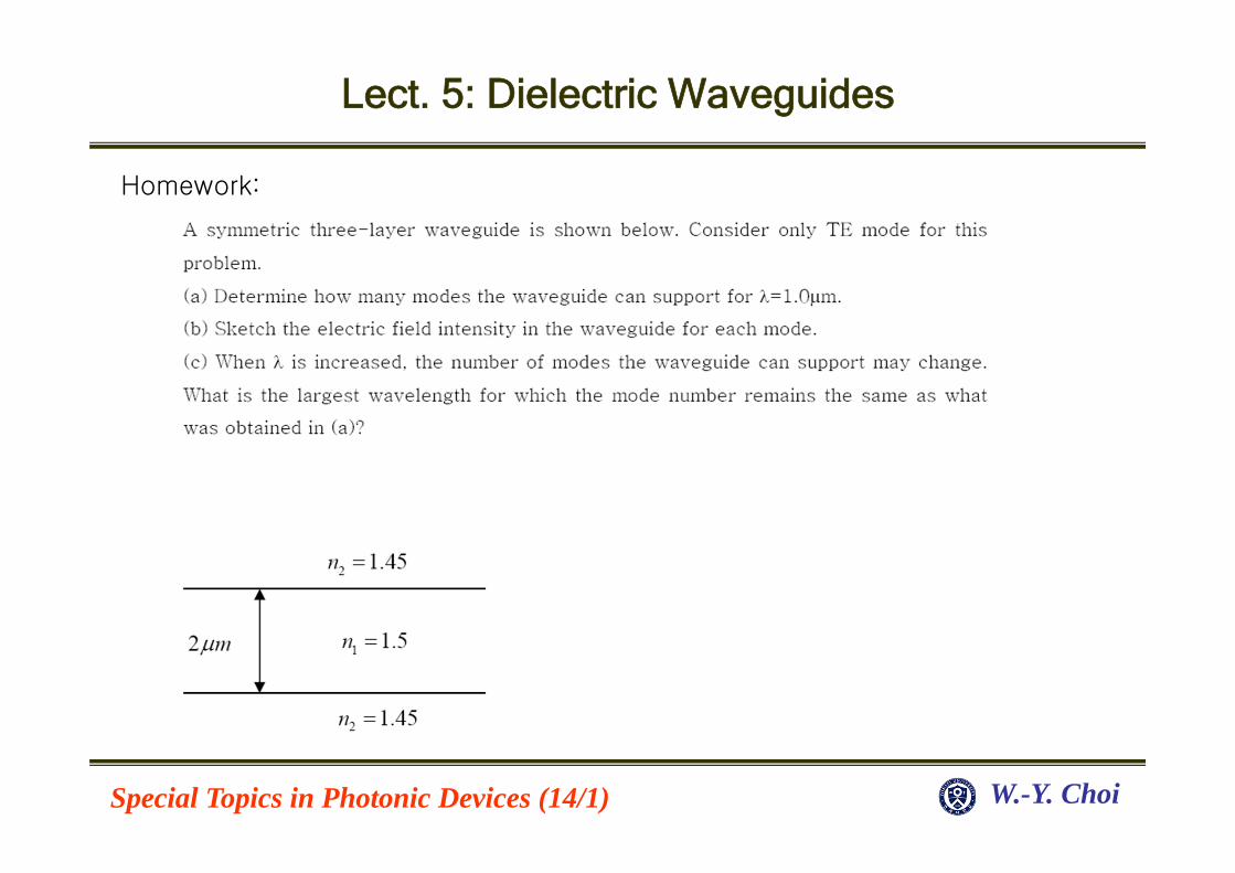
Lect. 5: Dielectric Waveguides
Special Topics in Photonic Devices (14/1) W.-Y. Choi
Guidance condition in a waveguide
2
22
0
( 1) ( 1) 1
2 2 and
(= ) ( )
y y yjk d jk d j k d
y y
z
e e emk d m kd
mk nkd
d
Metallic waveguide
,/ / ,/ / 1y yjk d jk de r e r
n2 cladding
d n1
n2 <n1
core
cladding
Dielectric waveguide (TIR)
,//,/ /Since ,jr e
,/ /2 2 2yk d m
,//2 2 1yj k d je e
,/ /Or yk d m
Lect. 5: Dielectric Waveguides
Special Topics in Photonic Devices (14/1) W.-Y. Choi
d
n2
n1
n2 <n1
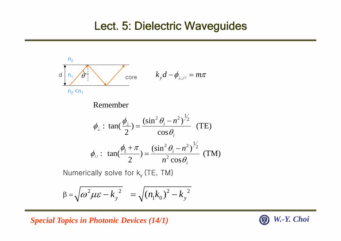
core ,/ / yk d m
Numerically solve for ky (TE, TM)
12 2 2
12 2 2||
/ / 2
Remember
(sin ) : tan( ) (TE)2 cos
(sin ): tan( ) (TM)2 cos
i
i
i
i
n
nn
2 2yk 2 2
1 0( ) yn k k
Lect. 5: Dielectric Waveguides
Special Topics in Photonic Devices (14/1) W.-Y. Choi
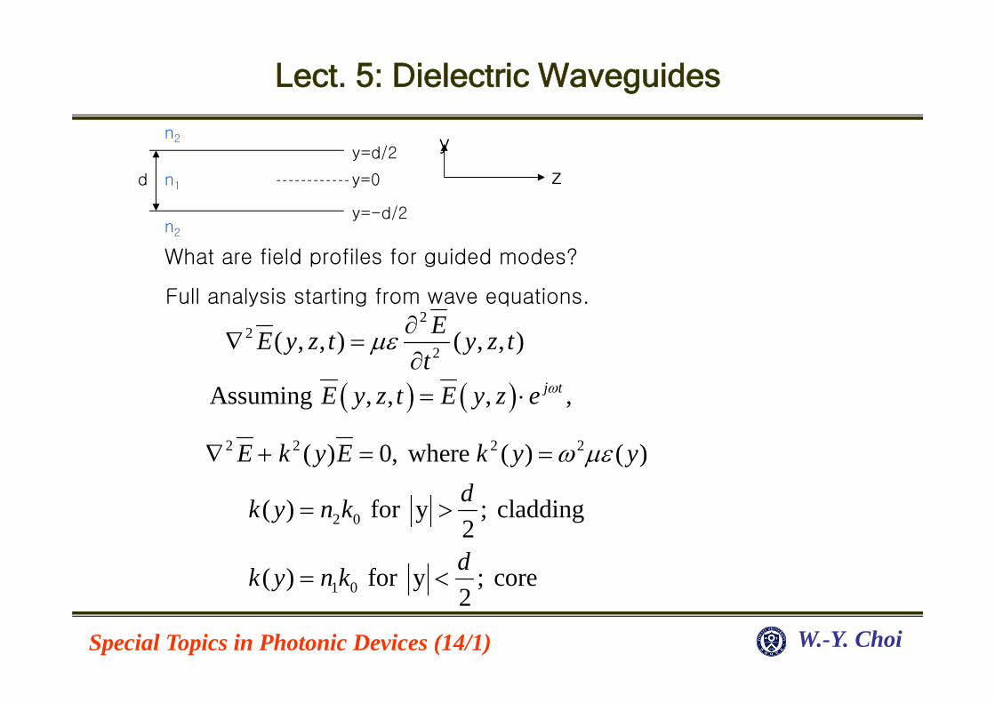
Full analysis starting from wave equations.
n2
d n1
n2
y=0
y=d/2
y=-d/2
y
z
22
2( , , ) ( , , )EE y z t y z tt
2 0
1 0
( ) for y ; cladding2
( ) for y ; core2
dk y n k
dk y n k
Assuming , , , , j tE y z t E y z e
2 2 2 2( ) 0, where ( ) ( )E k y E k y y
What are field profiles for guided modes?
Lect. 5: Dielectric Waveguides
Special Topics in Photonic Devices (14/1) W.-Y. Choi
Consider TE Solution.
d
n2
n1
n2
y=0
y=d/2
y=-d/2
y
z
( , ) ( ) j zE y z x E y e
2 2In core, ( ) 0 k y
22 2
2
( ) ( ( ) ) ( ) 0d E y k y E ydy
=> Eigen value equation. Solve for and ( ).E y
2 2In cladding, ( ) 0k y
2 2From ( ) 0,E k y E
=> ( ) ~ sin( ) or cos( )y yE y k y k y
2 2Sign of ( ( ) ) determines the solution type.k y 1 0 2 0We know n k n k
2 2 2( ) ,yk k y 2 21 0 ( )yk n k
=> ( ) ~ exp( ) or exp(- )E y y y 2 2 2( ) ,k y 2 2
2 0( )n k
Lect. 5: Dielectric Waveguides
Special Topics in Photonic Devices (14/1) W.-Y. Choi
d
n2
n1
n2
y=0
y=d/2
y=-d/2
y
z
Solutions
: ( ) exp( ) exp( )2
| | : ( ) sin( ) cos( )2
: ( ) exp( ) exp( )2
y y
dy E y A y B y
dy E y C k y D k y
dy E y E y F y
A=0 and F=0
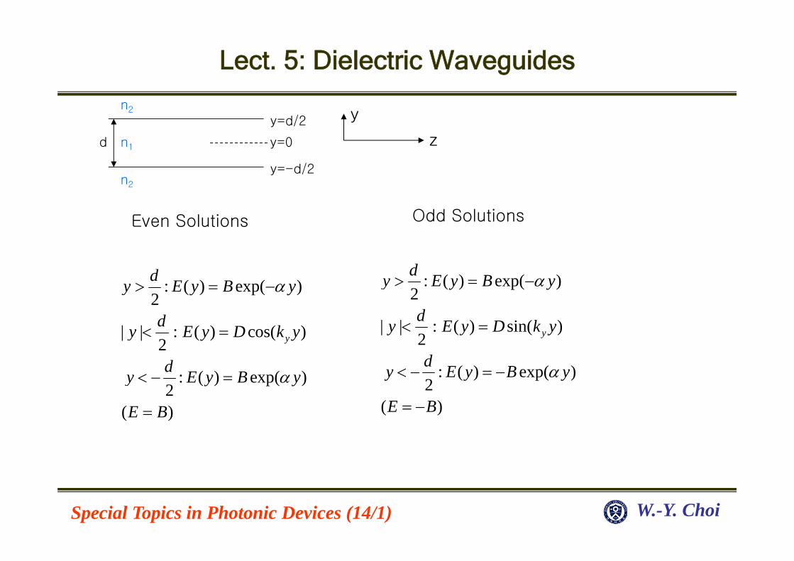
For easy analysis, divide the solutions into even and odd solutions
Lect. 5: Dielectric Waveguides
Special Topics in Photonic Devices (14/1) W.-Y. Choi
d
n2
n1
n2
y=0
y=d/2
y=-d/2
y
z
Even Solutions
: ( ) exp( )2
| | : ( ) cos( )2
: ( ) exp( )2
( )
y
dy E y B y
dy E y D k y
dy E y B y
E B
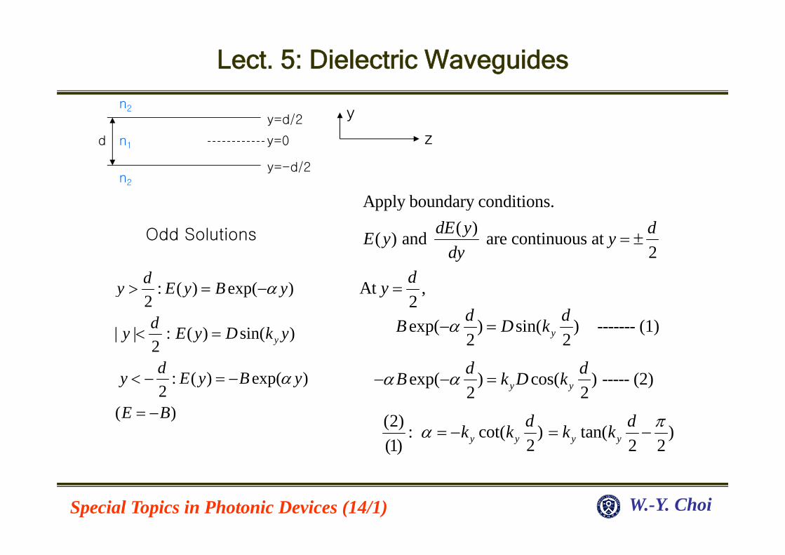
Odd Solutions
: ( ) exp( )2
| | : ( ) sin( )2
: ( ) exp( )2
( )
y
dy E y B y
dy E y D k y
dy E y B y
E B
Lect. 5: Dielectric Waveguides
Special Topics in Photonic Devices (14/1) W.-Y. Choi
d
n2
n1
n2
y=0
y=d/2
y=-d/2
y
z
Even Solutions
Apply boundary conditions:
: ( ) exp( )2
| | : ( ) cos( )2
: ( ) exp( )2
( )
y
dy E y B y
dy E y D k y
dy E y B y
E B
At ,2dy
( )( ) and are continuous at 2
dE y dE y ydy
(2) : tan( )(1) 2y y
dk k
exp( ) cos( ) ------- (1)2 2yd dB D k
exp( ) sin( ) ----- (2)2 2y yd dB k D k
Lect. 5: Dielectric Waveguides
Special Topics in Photonic Devices (14/1) W.-Y. Choi
d
n2
n1
n2
y=0
y=d/2
y=-d/2
y
z
Odd Solutions
: ( ) exp( )2
| | : ( ) sin( )2
: ( ) exp( )2
( )
y
dy E y B y
dy E y D k y
dy E y B y
E B
At ,2dy
Apply boundary conditions.( )( ) and are continuous at
2dE y dE y y
dy
exp( ) sin( ) ------- (1)2 2yd dB D k
(2) :(1)
exp( ) cos( ) ----- (2)2 2y yd dB k D k
cot( )2y ydk k tan( )
2 2y ydk k
Lect. 5: Dielectric Waveguides
Special Topics in Photonic Devices (14/1) W.-Y. Choi
d
n2
n1
n2
y=0
y=d/2
y=-d/2
y
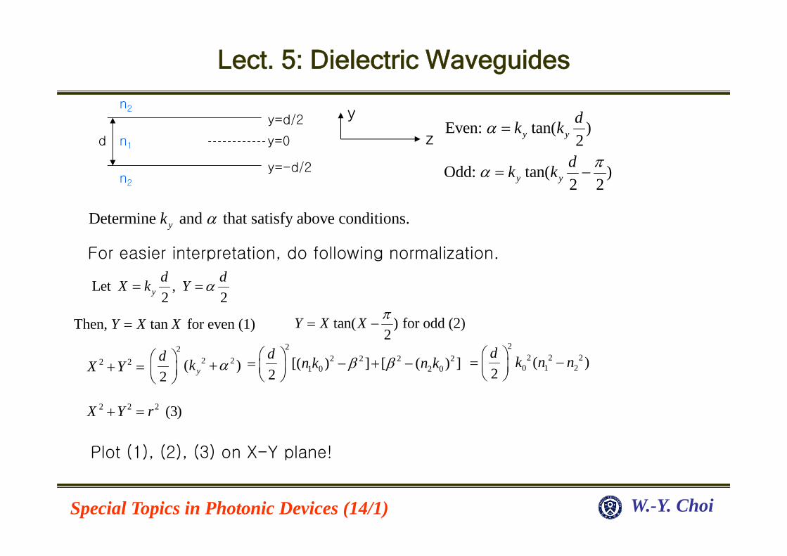
zEven: tan( )
2y ydk k
For easier interpretation, do following normalization.
Let ,2 2yd dX k Y
Plot (1), (2), (3) on X-Y plane!
Odd: tan( )2 2y ydk k
Determine and that satisfy above conditions.yk
Then, tan for even (1)Y X X tan( ) for odd (2)2
Y X X
2 2 X Y 2
2 2 2 21 0 2 0[( ) ] [ ( ) ]
2d n k n k
22 2( )
2 yd k
22 2 2
0 1 2( )2d k n n
2 2 2 (3)X Y r
Lect. 5: Dielectric Waveguides
Special Topics in Photonic Devices (14/1) W.-Y. Choi
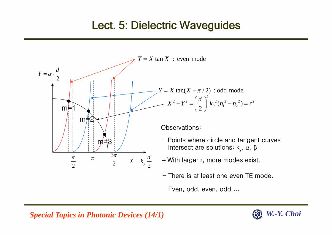
tan : even modeY X X
tan( / 2) : odd modeY X X
2ydX k
2dY
2 3
2
Observations:
22 2 2 2 2 2
0 1 2( )2dX Y k n n r
m=1
m=3
m=2
- Points where circle and tangent curvesintersect are solutions: ky, ,
With larger r, more modes exist.
- There is at least one even TE mode.
- Even, odd, even, odd …
Lect. 5: Dielectric Waveguides
Special Topics in Photonic Devices (14/1) W.-Y. Choi
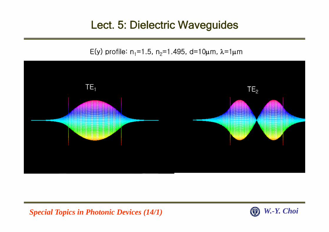
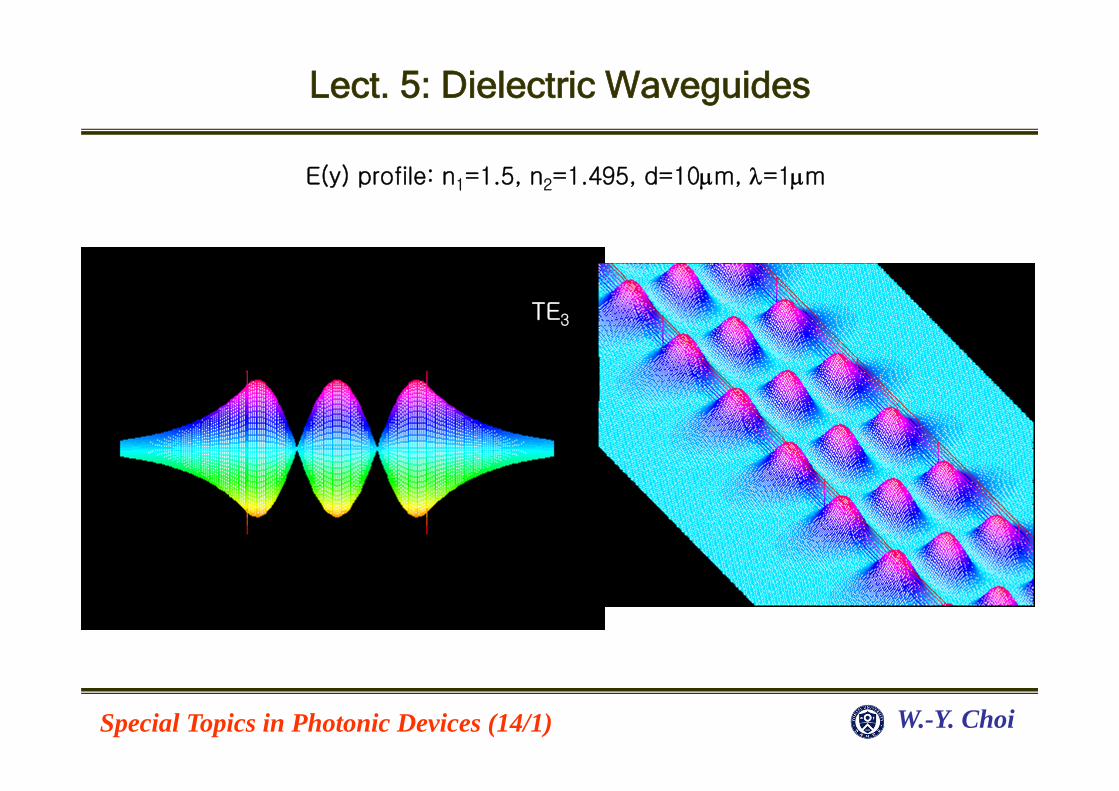
E(y) profile: n1=1.5, n2=1.495, d=10m, =1m
TE1 TE2
Lect. 5: Dielectric Waveguides
Special Topics in Photonic Devices (14/1) W.-Y. Choi
E(y) profile: n1=1.5, n2=1.495, d=10m, =1m
TE1 TE2TE3
Lect. 5: Dielectric Waveguides
Special Topics in Photonic Devices (14/1) W.-Y. Choi
How much power is confined within the core
22
2
2
( )Power inside core
Total Power( )
dy
dy
y
y
E y dy
E y dy
How does change for different modes?
- Effective index: neff= /k0
d n1
n2
n2
- Confinement factor:
How does neff changes for different modes?
Lect. 5: Dielectric Waveguides
Special Topics in Photonic Devices (14/1) W.-Y. Choi
+ +( ) ~ ( )in m m
mE y a E y
n2
n1
n2
( )inE y
For , use the fact that ( )'s are orthogonal.m ma E y
Partitioning of input field into different guided modes.
( ) ( )in mE y E y dy ~ ( ) ( )n n mn
a E y E y dy 2 ( )m ma E y dy
2
( ) ( )
( )in m
mm
E y E y dya
E y dy
Dot product between Ein(y) and Em(y)Or projection of Ein(y) into basis Em(y)
(Sturm-Liouville theory)
( ) ( ) 0 if m nE y E y dy m n
Lect. 5: Dielectric Waveguides
Special Topics in Photonic Devices (14/1) W.-Y. Choi
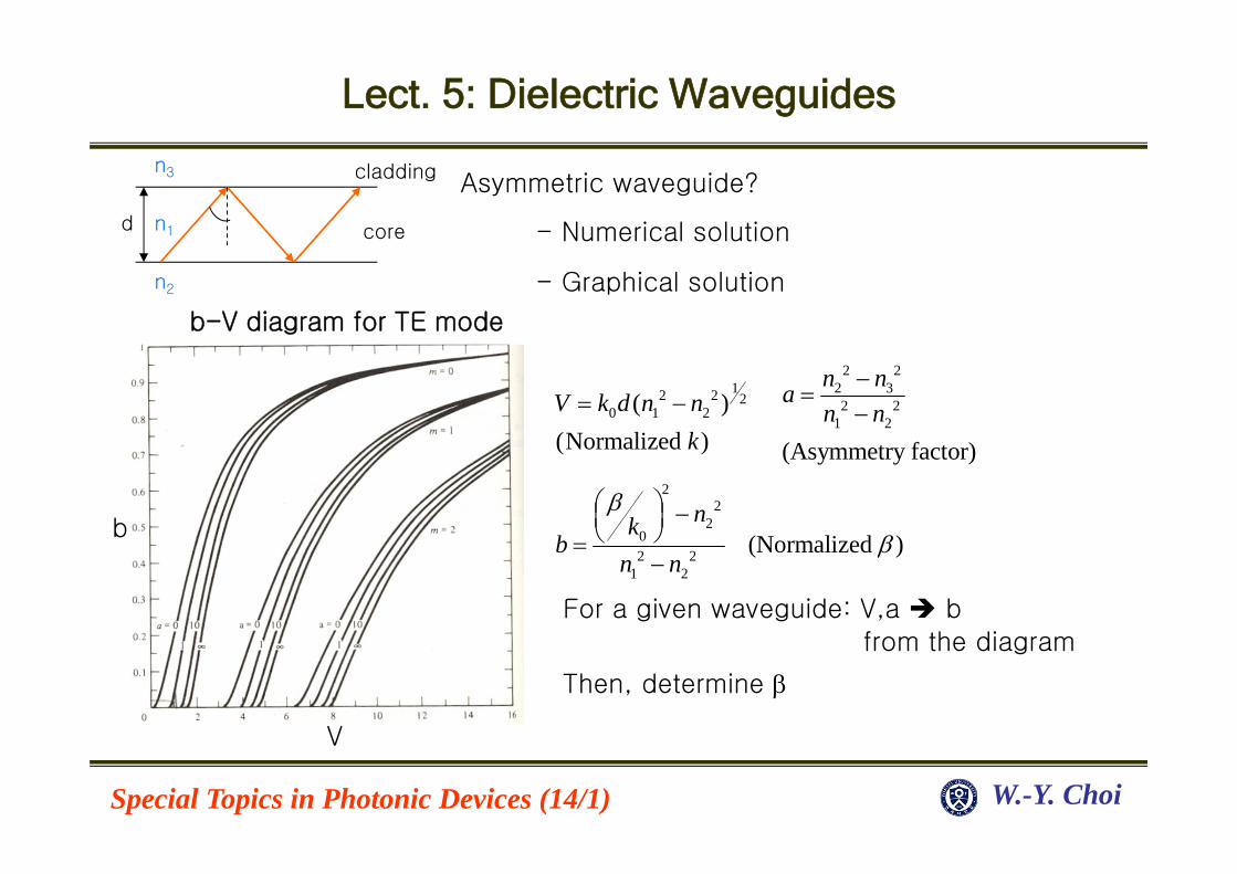
b-V diagram for TE mode
V
b
12 2 20 1 2( )
(Normalized )V k d n n
k
d
n3
n1 core
cladding
n2
Asymmetric waveguide?
- Graphical solution
2 22 32 2
1 2
(Asymmetry factor)
n nan n
22
202 2
1 2
(Normalized )nk
bn n
For a given waveguide: V,a b from the diagram
Then, determine
- Numerical solution
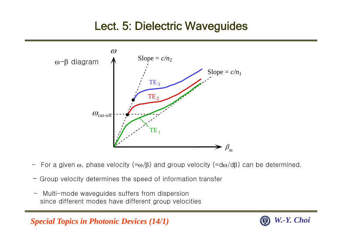
Lect. 5: Dielectric Waveguides
Special Topics in Photonic Devices (14/1) W.-Y. Choi
m
Slope = c/n2
Slope = c/n1
TE1
cut-off
TE2
TE3
Schematic dispersion diagram, vs. for the slab waveguide for various TE m. modes.cut–off corresponds to V = /2. The group velocity vg at any is the slope of the vs. curve at that frequency.