81
Wei 1 Lecture 7 MOSFET Devices and Circuits Gu-Yeon Wei Division of Engineering and Applied Sciences Harvard University [email protected]
| Date post: | 27-Oct-2015 |
| Category: |
Documents |
| Upload: | saujal-vaishnav |
| View: | 15 times |
| Download: | 0 times |

Wei 1
Lecture 7
MOSFET Devices and Circuits
Gu-Yeon WeiDivision of Engineering and Applied Sciences
Harvard [email protected]

ES154 - Lecture 7 - MOSFETsWei 2
Overview
• Reading– Chapter 6
• Supplemental Reading– Sedra&Smith: Chapter 5.1~5.4
• Background– Now that we have a basic understanding of semiconductors and PN
junctions, we will build on that knowledge to look at a transistor device called a MOSFET. This is the first of two transistors types that we will be studying in this course. Most modern ICs are built using these transistors. While they are commonly used to implement digital circuits, we will look at their analog characteristics and talk about how to build amplifiers with them.We begin with the physical structure and a qualitative understanding of how MOSFETs operate. We will derive some current-voltage equations for the transistor. We will also use band diagrams to provide some theoretical rigor to our initial qualitative understanding. Then, we will look at some non-ideal characteristics of the transistor. Lastly, we will analyze the DC operation of MOSFETs.

ES154 - Lecture 7 - MOSFETsWei 3
Enhancement-Type MOSFET
• Most widely used field effect transistor (enhancement type)• Let’s look at its structure and physical operation
– 3 terminal device (gate, source, drain)– Additional body (or bulk) terminal (generally at DC and not used for signals)– Two types:
• nMOS and pMOS

ES154 - Lecture 7 - MOSFETsWei 4
nMOS Transistor
• Four terminal device: gate, source, drain (and body)– No connection between the gate and drain/source (separated by oxide)– Voltage on gate controls current flow between source and drain
• Gate-oxide-body stack looks like a capacitor– Gate and body are conductors– SiO2 (oxide) is a good insulator– Called Metal-Oxide-Semiconductor (MOS) capacitor
• Gate no longer made out of metal, but poly

ES154 - Lecture 7 - MOSFETsWei 5
Basic nMOS Operation
• Body is commonly tied to ground (0V)• When the gate is at a low voltage (VG = 0):
– P-type body is at low voltage– Source-body and drain-body diodes are OFF (reverse bias)
• Depletion region between n+ and p bulk– No current can flow, transistor is OFF
ES154 - Lecture 7 - MOSFETsWei 6
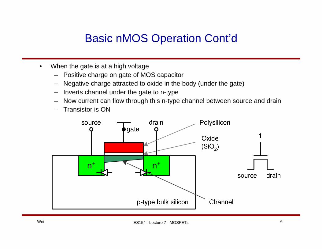
Basic nMOS Operation Cont’d
• When the gate is at a high voltage– Positive charge on gate of MOS capacitor– Negative charge attracted to oxide in the body (under the gate)– Inverts channel under the gate to n-type– Now current can flow through this n-type channel between source and drain– Transistor is ON

ES154 - Lecture 7 - MOSFETsWei 7
pMOS Transistor
• Similar to nMOS, but doping and voltages reversed– Body tied to high voltage (Vdd)– Gate low: transistor is ON
• inverted channel of positively charged holes– Gate high: transistor is OFF– Bubble indicates inverted behavior of the pMOS

ES154 - Lecture 7 - MOSFETsWei 8
MOSFET in More Detail
• An ON transistor passes a finite amount of current– Depends on terminal voltages and mode of operation– We will derive current-voltage (I-V) relationships
• To enhance our understanding of MOS devices, let’s take quick aside to look the characteristics of a MOS capacitor and at banddiagrams

ES154 - Lecture 7 - MOSFETsWei 9
Aside – MOS Capacitor
• Gate and body form a MOS cap• Operating modes
– Accumulation
– Depletion• Repels positive charge
– Inversion• Inversion layer forms under
the gate
ES154 - Lecture 7 - MOSFETsWei 10
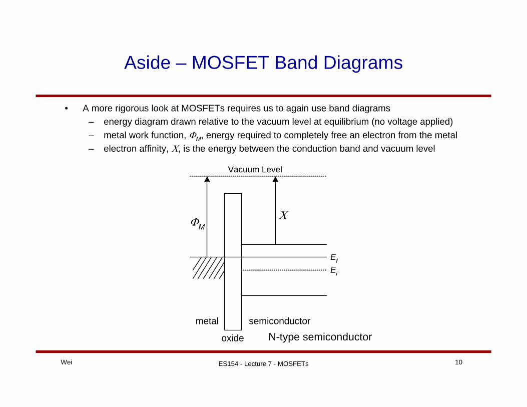
Aside – MOSFET Band Diagrams
• A more rigorous look at MOSFETs requires us to again use band diagrams– energy diagram drawn relative to the vacuum level at equilibrium (no voltage applied)– metal work function, ΦM, energy required to completely free an electron from the metal– electron affinity, Χ, is the energy between the conduction band and vacuum level
Vacuum Level
ΦMΧ
Ef
Ei
metal
oxide
semiconductor
N-type semiconductor

ES154 - Lecture 7 - MOSFETsWei 11
Aside – Block Charge diagram
• Provides information about the charge distribution inside a MOS structure– no charges at equilibrium– when bias is applied, charge appears within the metal and semiconductor at
the interfaces to the oxide• voltage drop across the oxide and there is an electric field due to the +Q and –Q
charge separated by the oxide
• We will use band diagrams and block charge diagrams to better understand how MOS devices work
position
charge
M O S
+Q
-Q

ES154 - Lecture 7 - MOSFETsWei 12
Aside – Applying Bias
• Look at a pMOS (n-type bulk) device and see how applying a bias on the gate affects the band and block charge diagrams
Accumulation(VG > 0)
M O S
+Q
-Q
Depletion(small VG < 0)
M O S
+Q
-Q
Onset ofInversion(VG = Vt)
M O S
+Q
-Q
Inversion(VG < Vt)
M O S
+Q
-Q
holes

ES154 - Lecture 7 - MOSFETsWei 13
Terminal Voltages
• The modes of operation depend on terminal voltages Vg, Vd, and Vs
– Vgs = Vg - Vs– Vgd = Vg - Vd– Vds = Vd - Vs = Vgs - Vgd
• Source and drain are symmetric diffusion terminals (transistors are symmetric devices)
– By convention, source is the terminal at the lower (higher) voltage for the nMOS(pMOS) transistor
– Hence, Vds > 0• nMOS body is grounded. First assume that
source is grounded as well• Three regions of operation
– Cutoff– Linear– Saturation

ES154 - Lecture 7 - MOSFETsWei 14
nMOS Cutoff Mode
• Vgs < Vt and so there is no channel• Source tied to body at 0V• Need a channel for current to flow Ids = 0

ES154 - Lecture 7 - MOSFETsWei 15
nMOS Linear Mode
• Vgs > Vt and so a channel forms underneath the gate– Vt is the threshold voltage that sets when a channel forms
• Current flows from d to s– Electrons flow from s to d
• Ids increases with Vds• Similar to a linear resistor

ES154 - Lecture 7 - MOSFETsWei 16
nMOS Saturation Mode
• Vds > Vgs – Vt and channel pinches off at the drain side– b/c Vgd < Vt at the drain side (no channel at drain side)
• We say current saturates and Ids is independent of Vds
• Transistor operates similar to a current source

ES154 - Lecture 7 - MOSFETsWei 17
I-V Characteristics
• In the Linear region of moderation, Ids depends on– How much charge is in the channel– How fast the charge is moving

ES154 - Lecture 7 - MOSFETsWei 18
Channel Charge
• MOS structure looks like a parallel plate capacitor while operating in inversion– Gate-oxide-channel

ES154 - Lecture 7 - MOSFETsWei 19
Carrier Velocity
• Charge is carried by e-
• Carrier velocity v is proportional to the lateral E-field between source and drain
• Time for carriers to cross the channel is

ES154 - Lecture 7 - MOSFETsWei 20
nMOS Linear I-V
• Combine the channel charge and velocity to find the current flow– Current = amount of charge in the channel / time it takes the
carriers to get across the channel

ES154 - Lecture 7 - MOSFETsWei 21
nMOS Saturation I-V
• If Vgd < Vt, channel pinches off near the drain– When Vds > Vdsat = Vgs – Vt
• Now, drain voltage no longer increases current and current saturates (Idsat)

ES154 - Lecture 7 - MOSFETsWei 22
Device Operation Review
• No gate voltage (vGS = 0)– Two back to back diodes both in reverse bias – no current flow between source and drain when voltage
between source and drain is applied (vDS >0)– There is a depletion region between the p (substrate)
and n+ source and drain regions• Apply a voltage on vGS > 0
– Positive potential on gate node pushes free holes away from the region underneath the gate and leave behind a negatively charged carrier depletion region
• transistor in depletion mode– As vGS increases, electrons start to gather at the surface
underneath the gate (onset of inversion)– When vGS is high enough, a n-type channel is induced
underneath the gate oxide where there are more electrons than holes (strong inversion)
• This induced region is called an inversion layer (or channel) and forms when vGS > some threshold voltage Vt and current can flow between S & D
• Transistor is in inversion mode
• When vDS = 0, no current flows between source and drain

ES154 - Lecture 7 - MOSFETsWei 23
Linear Operation
• With vGS large enough to induce a channel, apply a small potential vDS– Causes current to flow between source and drain (electrons flow from source to drain)– Magnitude of iD depends on density of electrons in channel which depends on vGS
(larger vGS = higher density of electrons)– Conductance of channel is proportional to vGS-Vt (called excess gate voltage or
effective voltage or gate overdrive)– Current is proportional to vGS-Vt and vDS that causes current to flow – i-v curve shows the transistor operates like a voltage-controlled linear resistor
• Notice iD = iS and iG = 0 due to the gate oxide
iD
vDS (small)
vGS <= Vt
vGS = Vt + V
vGS = Vt + 2 V
vGS = Vt + 3 V

ES154 - Lecture 7 - MOSFETsWei 24
Triode to Saturation Region
• Assume vGS is at a constant value > Vt and increase vDS– vDS appears as a voltage drop across the channel and at different points along the
channel, the voltage is different– Voltages between the gate and points along the channel are also different ranging from
vGS at the source to vGS-vDS at the drain• Induced channel is a function of voltage across the oxide at the different points and so channel
depth varies across the length of the transistor– i-v curve bends over as vDS increases due to the smaller channel depth – At vDS = vGS-Vt channel depth is almost zero at the drain side
• Current stays flat for higher voltages vDS > vGS-Vt• The transistor is said to now operate in the saturation region (not to be confused with the
saturation region in BJTs)

ES154 - Lecture 7 - MOSFETsWei 25
Saturation Region
• As vDS increases, the channel gets smaller and smaller on the drain side until vDS = vGS – Vtat which point the channel is said to be pinched off
– Increasing vDS beyond this point as little (ideally no) effect on the channel shape– Current remains constant and said to saturate– Transistor enters saturation at vDSsat = vGS – Vt
vDSchannelsource drain
vDS = 0
vDS >= vGS - Vt
ES154 - Lecture 7 - MOSFETsWei 26
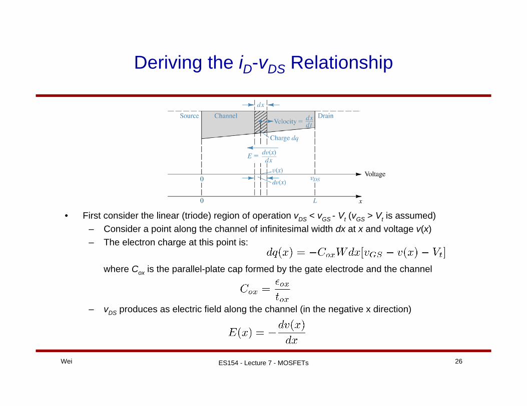
Deriving the iD-vDS Relationship
• First consider the linear (triode) region of operation vDS < vGS - Vt (vGS > Vt is assumed)– Consider a point along the channel of infinitesimal width dx at x and voltage v(x)– The electron charge at this point is:
where Cox is the parallel-plate cap formed by the gate electrode and the channel
– vDS produces as electric field along the channel (in the negative x direction)

ES154 - Lecture 7 - MOSFETsWei 27
• The electric field causes electron charge dq(x) to drift with a velocity dx/dt
– Where µn is the electron mobility in the channel– Current is the movement of charge and so…
• Rearrange the equation and integrate along the length of the channel
– Gives the current in the linear (triode) region:
– When vDS=vGS-Vt, we get the saturation current equation

ES154 - Lecture 7 - MOSFETsWei 28
nMOS I-V Summary
• Shockley 1st order model of transistors
– Cutoff
– Linear
– Saturation

ES154 - Lecture 7 - MOSFETsWei 29
+ Ideal Quadratic nMOS i-V
Vds
ids
Vg = 1.0V
Vg = 1.5V
Vg = 2.0V
Vg = 2.5V
saturation starts
linear saturation

ES154 - Lecture 7 - MOSFETsWei 30
nMOS and pMOS
• We’ve just seen how current flows in nMOS devices. A complementary version of the nMOS device is a pMOS shown above
– pMOS operation and current equations are the same except current is due to drift of holes
– The mobility of holes (µp) is lower than the mobility of electrons (µn) – Current is lower in pMOS devices given the same dimension and voltages.

ES154 - Lecture 7 - MOSFETsWei 31
Circuit Symbols
• We represent MOSFETs with the following symbols– The book specifies nMOS vs. pMOS with arrows (direction of current flow)– I will use bubbles b/c they are easier to distinguish quickly
• a digital circuit designer’s way of drawing symbols• These are symmetric devices and so drain and source can be used
interchangeably
nMOS or nFET pMOS or pFET

ES154 - Lecture 7 - MOSFETsWei 32
i-v Characteristics
• For small values of vDS, vDS2 is small and so near the origin, we can approximate
the transistor as a linear resistor

ES154 - Lecture 7 - MOSFETsWei 33
• We can get a relationship between iD and vGSwhen the transistor is in saturation
– Let vGS-Vt = VDS
• MOS vs. BJT– Current is quadratic with voltage in MOS vs.
exponential relationship in BJT

ES154 - Lecture 7 - MOSFETsWei 34
Some Non-Ideal Characteristics
• Channel-length modulation• Body effect• Velocity saturation

ES154 - Lecture 7 - MOSFETsWei 35
Channel-Length Modulation
• Like the Early effect in BJTs, there is an effect in MOSFETs that causes drain current to vary with vDS in saturation (finite output resistance)
• As vDS increases beyond vDSsat, the pinch off point moves away from the drain by ∆L and has the effect of changing the effective channel length in the transistor
– Account for this effect with a (1+λvDS) term in the saturation current equation

ES154 - Lecture 7 - MOSFETsWei 36
• Channel-length modulation makes the output resistance in saturation finite

ES154 - Lecture 7 - MOSFETsWei 37
Body Effect
• So far, we have been ignoring the substrate (or bulk or body) of the transistor and assumed that is it tied to the source. However, we cannot always make that assumption.
– In integrated circuits, the body is common to many MOS transistors and is connected to the most negative (positive) supply for nMOS (pMOS) transistors.
• The resulting reverse-bias voltage between the source and substrate affects device operation.
– Reverse bias will widen the depletion region and reduces channel depth – which can be modeled as changing the threshold voltage
where Vth0 is the threshold voltage when VSB=0, φf is a physical parameter, γ is a fabrication-process parameter…
γ is typically 0.5-V1/2
• As VSB increases, Vt increases which affects the transistor’s i-v characteristics

ES154 - Lecture 7 - MOSFETsWei 38
Temperature Effects
• Vt and mobility µn,p are sensitive to temperature– Vt decreases by 2-mV for every 1ºC rise in temperature– mobility µn,p decreases with temperature
• Overall, increase in temperature results in lower drain currents
ES154 - Lecture 7 - MOSFETsWei 39
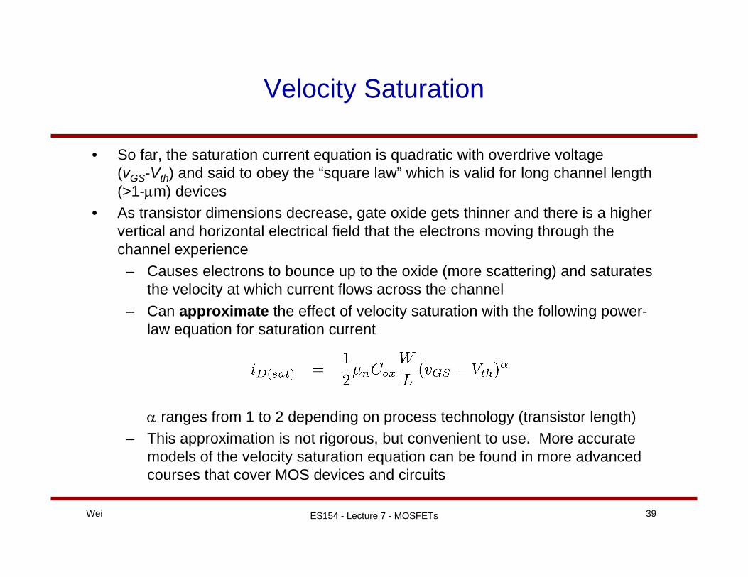
Velocity Saturation
• So far, the saturation current equation is quadratic with overdrive voltage (vGS-Vth) and said to obey the “square law” which is valid for long channel length (>1-µm) devices
• As transistor dimensions decrease, gate oxide gets thinner and there is a higher vertical and horizontal electrical field that the electrons moving through the channel experience
– Causes electrons to bounce up to the oxide (more scattering) and saturates the velocity at which current flows across the channel
– Can approximate the effect of velocity saturation with the following power-law equation for saturation current
α ranges from 1 to 2 depending on process technology (transistor length)– This approximation is not rigorous, but convenient to use. More accurate
models of the velocity saturation equation can be found in more advanced courses that cover MOS devices and circuits

ES154 - Lecture 7 - MOSFETsWei 40
Real nMOS i-V Curve
• i-v curves of nMOS transistor in 0.5-µm CMOS technology
• W = 2.5-µm, L = 0.6-µm

ES154 - Lecture 7 - MOSFETsWei 41
Depletion-type MOSFETs
• Depletion-type MOSFETs have a channel with zero vGS (symbol is drawn with channel)
– must apply negative vGS to “turn off” device– Can be used as resistor loads (will see later)

ES154 - Lecture 7 - MOSFETsWei 42
MOSFET at DC Example
• Current Mirror– What is vGS?– How is ID related to ISRC?– What is ID vs. VD?
VD
IDISRC
vGS

ES154 - Lecture 7 - MOSFETsWei 43
MOSFET Amplifier
• The MOSFET can be configured to operate as an amplifier. One of the simplest amplifier configurations one can build with a MOSFET is a common-source amplifier.
• Requirements for proper operation– MOSFET must operate in saturation
• Depends on RD and voltage biasing VGS

ES154 - Lecture 7 - MOSFETsWei 44
Load Line
• Use a load line to see the operating point of the transistor w.r.t. RD and VGS

ES154 - Lecture 7 - MOSFETsWei 45
DC Biasing
• There are many ways to bias the CS nMOS Amp. Here are two ways…
• What is VIN (or VGS) for the circuit on the right?• What is the cap for?

ES154 - Lecture 7 - MOSFETsWei 46
DC Bias
• First bias MOSFET in saturation region (equivalent to active region in BJTs) to operate as an amplifier
– set vgs = 0 and find ID (for now, assume λ=0)
– To be in saturation,
– Apply a small signal, vgs, to the gate

ES154 - Lecture 7 - MOSFETsWei 47
• Three components of iD
– First term = DC current– Second term = current proportional to vgs
– Third term = undesired nonlinear distortion• Make vgs small to reduce effect of third term
– This is the small-signal condition and let’s us use the following approximation
– and we can relate id to vgs with a transconductance

ES154 - Lecture 7 - MOSFETsWei 48
• Small-Signal Voltage Gain (vd/vgs)
– This gain equation hold for small signals– Notice that the output is 180° out of phase w.r.t. the input
• Again, we can separate out the DC bias conditions and the small-signal operation of the circuit
– Look at the small-signal equivalent circuit for a MOSFET biased in the saturation region

ES154 - Lecture 7 - MOSFETsWei 49
Small-Signal Equivalent Circuit
• A MOSFET operates like voltage controlled current source (for small signals)
– Like the Early effect in the BJT, channel length modulation results in an output resistance, ro
– where VA = 1/λ• When using small-signal equivalent circuits, all DC sources are set to 0 since
they do not change
ES154 - Lecture 7 - MOSFETsWei 50
Transconductance
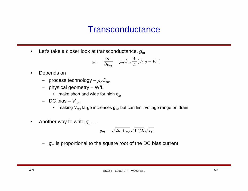
• Let’s take a closer look at transconductance, gm
• Depends on – process technology – µnCox
– physical geometry – W/L • make short and wide for high gm
– DC bias – VGS
• making VGS large increases gm, but can limit voltage range on drain
• Another way to write gm …
– gm is proportional to the square root of the DC bias current

ES154 - Lecture 7 - MOSFETsWei 51
T-Model
• Sometimes easier to analyze circuits using a different model• T-Model and π-Model are equivalent circuits
– Resistance looking into the source is 1/gm
– Resistance looking into G is still ∞ since ig=0
T-Model π-Model

ES154 - Lecture 7 - MOSFETsWei 52
Body Effect
• Body Effect– We saw that the substrate bias VBS affects Vt which has the effect
of influencing current like another gate
vgs vbs
gmvgs gmbvbs
G
S
D
B
ro

ES154 - Lecture 7 - MOSFETsWei 53
Example 1: CS Amp with Resistor Biasing
• Let’s look at another CS amplifier example…– What does the mid-band small-signal
equivalent circuit look like?– What is vbs?– What is Rin seen by the source?– What is Rout?
vin
VDD
RDR1
R2
vDSRs
Rs
vin R1||R2 vgs
gmvgs
vds
gmbvbs
ro RD

ES154 - Lecture 7 - MOSFETsWei 54
Example 1 cont’d
• Use the small-signal equivalent circuit to figure out small-signal gain, Rin and Rout

ES154 - Lecture 7 - MOSFETsWei 55
In Pursuit of More Gain
• How can we make the gain bigger?– Can we arbitrarily increase RD?
– Would like to make the load line shallow and shifted up

ES154 - Lecture 7 - MOSFETsWei 56
Example 2: Common-Source Amplifier w/ Active Load
• Active load – uses current source instead of load resistor
– Biasing so that Q2 in saturation and its output resistance is the effective resistor load for Q1
• Combine the I-V curves

ES154 - Lecture 7 - MOSFETsWei 57
• Look at the Voltage Transfer Characteristics (VTC) of the circuit– Operates like a high-gain amplifier (steep slope) in region III

ES154 - Lecture 7 - MOSFETsWei 58
• CS Amplifier low-frequency small-signal model
• What is the voltage gain?
vgs
gmvgsro1 ro2 vovi
Output Resistance ofCurrent Source
• What are Rin and Rout?

Wei 59
Supplemental Slides on MOS Transistors from CS148

ES154 - Lecture 7 - MOSFETsWei 60
Fabricating CMOS Transistors
• CMOS transistors are fabricated on a silicon wafer• Lithography process similar to printing press• On each step, different materials are deposited and etched
– Multiple steps per layer drawn in layout• Understand by viewing both top and cross section of wafer in a
simplified manufacturing process

ES154 - Lecture 7 - MOSFETsWei 61
Inverter Cross Section
• Typically use p-type substrate (wafer) where nMOS transistors are drawn
• Need to create n-well for body of pMOS transistors

ES154 - Lecture 7 - MOSFETsWei 62
Well and Substrate Taps
• Substrate (p-type) must be tied to Gnd and nwell tied to Vdd• Metal to lightly-doped semiconductor forms a poor contact connection
(Shottky Diode)• Use heavily doped well and substrate contacts (taps)

ES154 - Lecture 7 - MOSFETsWei 63
Inverter Mask Set
• Transistors and wires are defined by masks• Cross section taken along dashed line

ES154 - Lecture 7 - MOSFETsWei 64
Detailed Mask Views
• Six masks– nwell
– polysilicon (gate)
– n+ diffusion
– p+ diffusion– contact
– metal

ES154 - Lecture 7 - MOSFETsWei 65
Fabrication Steps
• Start with blank wafer• Build inverter from bottom up• First step will be form the nwell
– Cover wafer with protective layer of SiO2 (oxide)– Remove layer where nwell should be– Implant or diffuse n dopants into exposed portion of wafer– Strip off SiO2
• Grow SiO2 on top of Si wafer– 900-1200 C with H2O or O2 in oxidation furnace

ES154 - Lecture 7 - MOSFETsWei 66
Photoresist
• Spin on photoresist– Photoresist is a light-sensitive organic polymer– Softens where exposed to light

ES154 - Lecture 7 - MOSFETsWei 67
Lithography
• Expose photoresist through nwell mask• Strip off exposed photoresist

ES154 - Lecture 7 - MOSFETsWei 68
Etch
• Etch oxide with hydrofluoric acid (HF)– Seeps through skin and eats bone… not something you want to
have around in your bathroom– Only attacks oxide where photoresist has been exposed
ES154 - Lecture 7 - MOSFETsWei 69
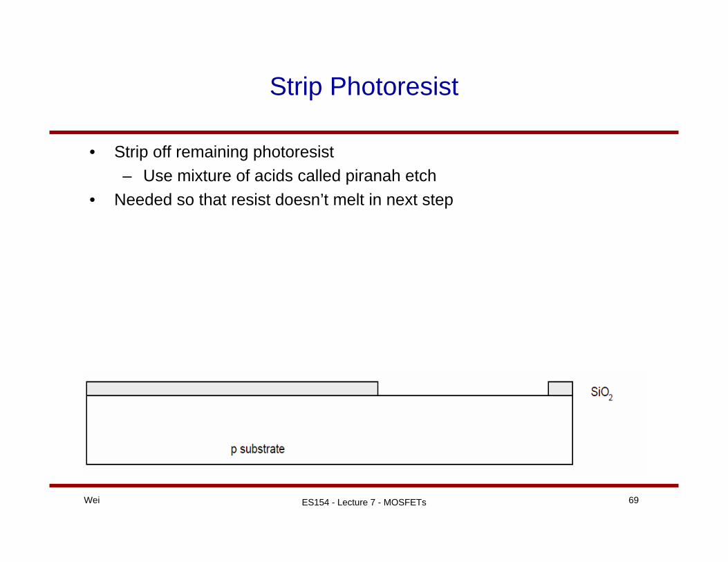
Strip Photoresist
• Strip off remaining photoresist– Use mixture of acids called piranah etch
• Needed so that resist doesn’t melt in next step

ES154 - Lecture 7 - MOSFETsWei 70
nwell
• Nwell is formed with diffusion or ion implantation• Diffusion
– Place wafer in a furnace with arsenic gas– Heat until As atoms diffuse into exposed Si
• Ion implantation– Blast wafer with beams of As ions– Ions blocked by SiO2, only enter where Si exposed

ES154 - Lecture 7 - MOSFETsWei 71
Strip Oxide
• Strip off the remaining oxide with HF• Back to bare wafer with nwell• Subsequent steps involve similar series of steps

ES154 - Lecture 7 - MOSFETsWei 72
Polysilicon
• Depost very thin later of gate oxide– < 20 angstoms (6-7 atomic layers)
• Chemical vapor deposition (CVD) of silicon layer– Place wafer in furnace with Silane gas (SiH4)– Forms many small Si crystals called polysilicon– Heavily doped to be a good conductor

ES154 - Lecture 7 - MOSFETsWei 73
Polysilicon patterning
• Use same lithography process to pattern polysilicon

ES154 - Lecture 7 - MOSFETsWei 74
Self-Aligned Process
• Use oxide and masking to expose where n+ dopants should be diffused or implanted
• N-diffusion forms nMOS source, drain, and nwell contact

ES154 - Lecture 7 - MOSFETsWei 75
N-diffusion
• Pattern oxide and form n+ regions• Self-aligned process where gate blocks diffusion• Polysilicon is better than metal for self-aligned gates b/c it doesn’t melt
during later processing

ES154 - Lecture 7 - MOSFETsWei 76
N-diffusion cont’d
• Historically, dopants were diffused• Usually ion implantation is used today• But regions still called diffusion

ES154 - Lecture 7 - MOSFETsWei 77
N-diffusion cont’d
• Strip off oxide to complete patterning step

ES154 - Lecture 7 - MOSFETsWei 78
P-Diffusion
• Similar set of steps to form p+ diffusion regions for pMOS source and drain and substrate contact
ES154 - Lecture 7 - MOSFETsWei 79
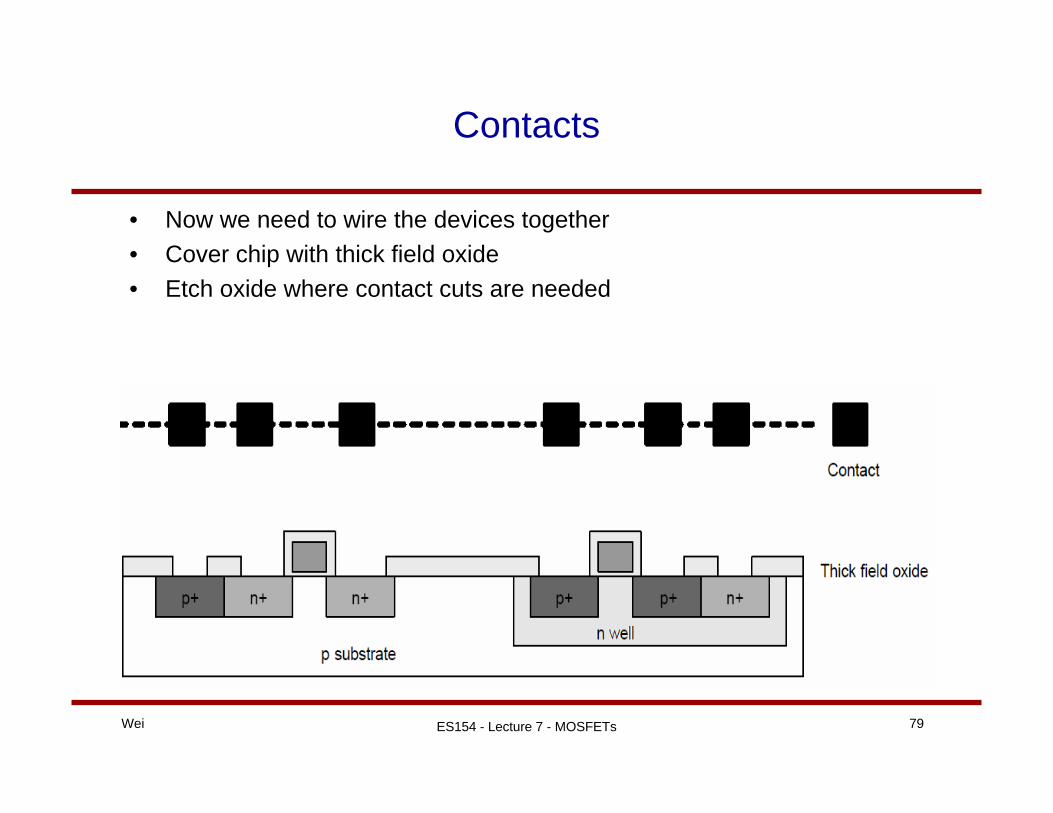
Contacts
• Now we need to wire the devices together• Cover chip with thick field oxide• Etch oxide where contact cuts are needed

ES154 - Lecture 7 - MOSFETsWei 80
Metalization
• Sputter on aluminum over entire wafer• Patter to remove excess metal, leaving wires

ES154 - Lecture 7 - MOSFETsWei 81
Layout
• Chips are specified with set of masks• Minimum dimensions of masks determine transistor size (and
hence speed, cost, and power)• Feature size f = distance between source and drain
– Set by minimum width of polysilicon (minimum channel length)
• Feature size improves 30% every three years or so• Normalize for feature size when describing design rules• Express rules in terms of λ = f/2
– We will use \lambda = 0.3µm in 0.6 µm process (actually a 0.5 µm process but drawn as 0.6 µm)
• Next time: Learn SUE and Magic to draw your own layouts!