13
ECE 3040 - Dr. Alan Doolittle Georgia Tech Lecture 12 P-N Junction Diodes: Part 2 How do they work? (A little bit of math) Reading: Pierret 6.1

ECE 3040 - Dr. Alan DoolittleGeorgia Tech
Lecture 12
P-N Junction Diodes: Part 2
How do they work? (A little bit of math)
Reading:
Pierret 6.1

ECE 3040 - Dr. Alan DoolittleGeorgia Tech
Fig Pierret 5.5
Space Charge or Depletion Region
Movement of electrons and holes when forming the junctionCircles are charges free to move (electrons and holes)
Squares are charges NOT free to move (ionized donor or acceptor atoms)
High electron Concentration
High hole Concentration
Electron diffusion
Hole diffusion
Local region of positive charge
due to imbalance in
electron-donor concentrations
Local region of negative
charge due to imbalance in
hole-acceptor concentrations
ECE 3040 - Dr. Alan DoolittleGeorgia Tech
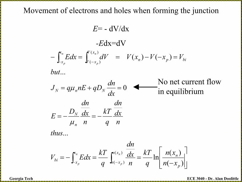
Movement of electrons and holes when forming the junction
E= - dV/dx
-Edx=dV
−==−=
−=−=
=+=
=−−==−
∫∫
∫∫
−−
−−
)()(ln
...
0
...
)()(
)(
)(
)(
)(
p
nxn
xn
x
xbi
n
N
NnN
bipn
xV
xV
x
x
xnxn
qkT
ndxdn
qkTEdxV
thusndxdn
qkT
ndxdn
DE
dxdnqDnEqJ
but
VxVxVdVEdx
n
p
n
p
n
p
n
p
µ
µNo net current flow in equilibrium

ECE 3040 - Dr. Alan DoolittleGeorgia Tech
=
=
−=
2
2
ln
ln)(
)(ln
i
DAbi
A
i
D
p
nbi
nNN
qkTV
NnN
qkT
xnxn
qkTV
Movement of electrons and holes when forming the junction
For NA=ND=1015/cm-3 in silicon at room temperature, Vbi~0.6 V*
For a non-degenerate semiconductor, |-qVbi|<|Eg|
*Note to those familiar with a diode turn on voltage: This is not the diode turn on voltage! This is the voltage required to reach a flat band diagram and sets an upper limit (typically an overestimate) for the voltage that can be applied to a diode before it burns itself up.

ECE 3040 - Dr. Alan DoolittleGeorgia Tech
Movement of electrons and holes when forming the junctionDepletion Region Approximation
++++++++++++++++++++++
- - - - - - - - - - - - - - - - - - - -
Depletion Region Approximation states that approximately no free carriers exist in the space charge region and no net charge exists outside of the depletion region (known as the quasi-neutral region). Thus,
regionechspacethewithinNNKq
dxdEbecomes
regionneutralquasithewithinNNnpKq
KdxdE
ADoS
ADoSoS
arg)(
...
0)(
−=
−=−+−==
ε
εερ

ECE 3040 - Dr. Alan DoolittleGeorgia Tech
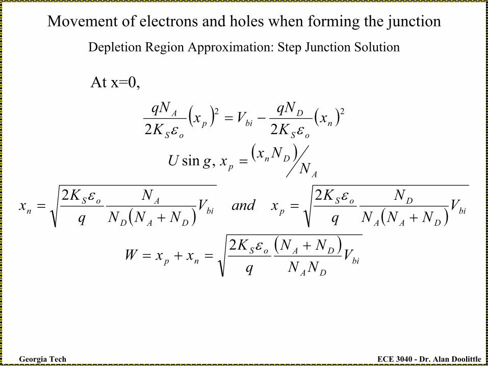
Movement of electrons and holes when forming the junctionDepletion Region Approximation: Step Junction Solution
Fig. 5.9 a and b
≥−≤
≤≤
≤≤−−
=
≥−≤≤≤
≤≤−−=
np
noS
D
poS
A
np
nD
pA
xxandxxfor
xxforKqN
xxforKqN
dxdE
thus
xxandxxforxxforqNxxforqN
0
0
0
,
00
0
ε
ε
ρ
oSKdxdE
ερ
=
Where we have used:

ECE 3040 - Dr. Alan DoolittleGeorgia Tech
( )
( ) nnoS
D
n
x
xoS
DxE
ppoS
A
p
x
xoS
AxE
xxforxxKqNxE
xxfordxKqNdE
and
xxforxxKqNxE
xxfordxKqNdE
n
p
≤≤−−
=
≤≤=
≤≤−+−
=
≤≤−−
=
∫∫
∫∫ −
0)(
0''
0)(
0''
0
)(
)(
0
ε
ε
ε
ε
Movement of electrons and holes when forming the junctionDepletion Region Approximation: Step Junction Solution
Since E(x=0-)=E(x=0+)
NAxp=NDxn

ECE 3040 - Dr. Alan DoolittleGeorgia Tech
( )
( )
( )
( )
( )
( )
≤≤−−
≤≤−+=
≤≤−=
≤≤−+=
≤≤−
≤≤−+=
−=
∫∫
∫∫ −
nnoS
Dbi
ppoS
A
n
x
x noS
DV
xV
p
x
x poS
AxV
nnoS
D
ppoS
A
xxforxxKqN
V
xxforxxKqN
xV
xxfordxxxKqNdV
xxfordxxxKqN
dV
or
xxforxxKqN
xxforxxKqN
dxdV
dxdVE
nBi
p
02
02)(
0'''
0'''
,
0
0
2
2
)(
)(
0
ε
ε
ε
ε
ε
ε
Movement of electrons and holes when forming the junctionDepletion Region Approximation: Step Junction Solution
V=VBi
V=0
ECE 3040 - Dr. Alan DoolittleGeorgia Tech
( ) ( )
( )
( ) ( )( )
biDA
DAoSnp
biDAA
DoSpbi
DAD
AoSn
A
Dnp
noS
Dbip
oS
A
VNNNN
qK
xxW
VNNN
NqK
xandVNNN
NqK
x
NNxxgU
xKqN
VxKqN
+=+=
+=
+=
=
−=
ε
εε
εε
2
22
,sin
2222
Movement of electrons and holes when forming the junctionDepletion Region Approximation: Step Junction Solution
At x=0,

ECE 3040 - Dr. Alan DoolittleGeorgia Tech
Movement of electrons and holes when forming the junctionDepletion Region Approximation: Step Junction Solution
Vbi
Vbi
|VA|Vbi
|VA|
Vbi
VA=0 : No Bias VA<0 : Reverse Bias VA>0 : Forward Bias

ECE 3040 - Dr. Alan DoolittleGeorgia Tech
Movement of electrons and holes when forming the junctionDepletion Region Approximation: Step Junction Solution
( ) ( ) ( ) ( )
( ) ( )AbiDA
DAoSnp
AbiDAA
DoSpAbi
DAD
AoSn
VVNNNN
qK
xxW
VVNNN
NqK
xandVVNNN
NqK
x
−+
=+=
−+
=−+
=
ε
εε
2
22
Thus, only the boundary conditions change resulting in direct replacement of Vbi with (Vbi-VA)

ECE 3040 - Dr. Alan DoolittleGeorgia Tech
Movement of electrons and holes when forming the junctionStep Junction Solution: What does it mean?
Consider a p+ -n junction (heavily doped p-side, normal or lightly doped n side).

ECE 3040 - Dr. Alan DoolittleGeorgia Tech
Movement of electrons and holes when forming the junctionStep Junction Solution: What does it mean?
Efp-Efn=-qVA
Fermi-level only applies to equilibrium (no current flowing)
Majority carrier Quasi-fermi levels


