40
Lecture 13 Lecture by John O'Donnell, used with permission. 1 CS1Q Computer Systems Lecture 13 Simon Gay
| Date post: | 27-Dec-2015 |
| Category: |
Documents |
| Upload: | cory-robertson |
| View: | 218 times |
| Download: | 0 times |

Lecture 13 Lecture by John O'Donnell, used with permission. 1
CS1Q Computer SystemsLecture 13
Simon Gay

Lecture 13 Lecture by John O'Donnell, used with permission. 2
Where we are
Global computing: the Internet
Networks and distributed computing
Application on a single computer
Operating System
Architecture
Digital Logic
Electronics
Physics
A general impression of thelowest levels of hardware

The Lowest Level of Hardware:
Transistors and ChipsJohn O'Donnell
Computing Science DepartmentUniversity of Glasgow
Copyright © 2002 John O’Donnell
Used, with permission, by Simon Gay.
Computer Systems

Lecture 13 Lecture by John O'Donnell, used with permission. 4
And Now forSomething Completely Different!
How do logic gates work anyway?
A brief introduction…
to VLSI electronics
A logic gate is actually a circuit comprising primitive components (MOSFET pass transistors) and we can understand (roughly) how these work just using a little elementary physics

Lecture 13 Lecture by John O'Donnell, used with permission. 5
Physics Background
Atoms
Electrons have negative charge
Nucleus contains protons with positive charge – Like charges repel– Unlike charges attract

Lecture 13 Lecture by John O'Donnell, used with permission. 6
Chemistry Background
• Electron Shells– The electrons around a nucleus are grouped into
shells. Each shell has an ideal number of electrons that will fit into it, and the atom “likes” to have the outer shell filled
• Covalent Chemical Bonds– Two atoms with partially filled outer shells can
“share” some electrons; they bond together

Lecture 13 Lecture by John O'Donnell, used with permission. 7
Insulators and Conductors
• If an atom has just enough electrons to fill the outer shell exactly, then electricity (moving electrons) can’t go through it. It’s an insulator.
• If an atom has only a few electrons in a big shell far from the nucleus, it’s easy to get those electrons moving. It’s a conductor (silver, copper, gold, …)

Lecture 13 Lecture by John O'Donnell, used with permission. 8
Semiconductors
• Silicon is a semiconductor, halfway between an insulator and a conductor.
• Its outer shell wants to have 8 electrons, but the Silicon atom provides only 4.
• The atom forms covalent bonds with its neighbors, ending with filled shells.
• This is a silicon crystal, which is a good insulator
Lecture 13 Lecture by John O'Donnell, used with permission. 9
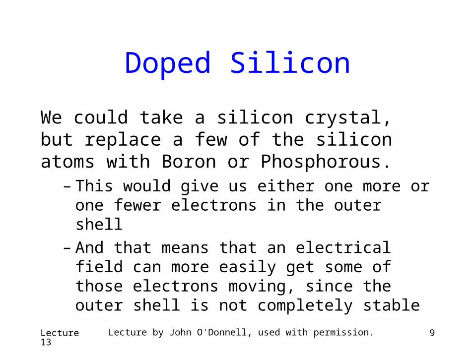
Doped Silicon
We could take a silicon crystal, but replace a few of the silicon atoms with Boron or Phosphorous.
– This would give us either one more or one fewer electrons in the outer shell
– And that means that an electrical field can more easily get some of those electrons moving, since the outer shell is not completely stable

Lecture 13 Lecture by John O'Donnell, used with permission. 10
N and P Type Silicon
• Pure silicon is an insulator, but it can be doped, turning it into:– N type silicon, a semiconductor with negative
charge carriers (called free electrons)– P type silicon, a semiconductor with positive
charge carriers (called holes). These are spots where an electron would like to be (would lower the energy) but isn’t.

Lecture 13 Lecture by John O'Donnell, used with permission. 11
Negative Charge Carriers
-
- -
-- -
-
N type

Lecture 13 Lecture by John O'Donnell, used with permission. 12
Positive Charge Carriers
+
+
+
+
+
+
+
In reality, the only movable charge carriers are negative electrons. However, they behave as if there are holes that can move, and the holes act as if they have a positive charge.
P type

Lecture 13 Lecture by John O'Donnell, used with permission. 13
Junctions
-+
+
+
+
+
+
+
- -
-- -
-
a PN junction is formed when a P-type region is fabricated adjacent to an N-type region
N typeP type

Lecture 13 Lecture by John O'Donnell, used with permission. 14
Forward Biased Junction
-+
+
++
+
+
+
---
- --
+
An electron annihilates a hole, enabling further electrons to move left and further holes to move right
+
New hole injected by+ power supply
-
Newly injectedelectron
Current flows steadily!
P type N type

Lecture 13 Lecture by John O'Donnell, used with permission. 15
+
Reverse Biased Junction
++ +
+++ -
-
---
- +
There are no free charge carriers near the junction, so it becomes an insulating crystal
+-
No current flows acrossthe junction!
P type N type

Lecture 13 Lecture by John O'Donnell, used with permission. 16
The Junction Diode
A diode allows current to flow across it in one direction but not the other
A PN junction does exactly that!

Lecture 13 Lecture by John O'Donnell, used with permission. 17
N-Type Wires
Top view of chip
Each of the four N-type wires carries a signalsafely; a short circuit is impossible because itwould have to cross a reverse biased junction

Lecture 13 Lecture by John O'Donnell, used with permission. 18
Integrated Circuits
• Long ago, circuits were built by connecting the components one at a time, soldering in wires one at a time
• Using channels to hold wires suggests a new idea– Fabricate many components together on a chip,
along with all their wires– The wiring is integrated with the components

Lecture 13 Lecture by John O'Donnell, used with permission. 19
Metal—Oxide—Semiconductor
Metal: a layer of aluminium
Silicon dioxide—glass—an insulator
Semiconductor—doped silicon
This is called MOS technology
Side view

Lecture 13 Lecture by John O'Donnell, used with permission. 20
Neutral Gate
The “gate”
insulation
The “substrate”
If the gate is not charged, it has no effect on the substrate
+
+
+
+ +

Lecture 13 Lecture by John O'Donnell, used with permission. 21
Positive Gate, P-type Substrate
Positive power supply
Free electrons in the substrate are attracted to the region under the gate, where they are stuck because of the insulator
If the gate is positively charged, it temporarily transforms part of the P-type substrate into N-type
+++ + +

Lecture 13 Lecture by John O'Donnell, used with permission. 22
Gap in a Wire
a b
Side view
Top view
No current can flow between a and b, in either direction, since it would have to cross a reverse biased junction

Lecture 13 Lecture by John O'Donnell, used with permission. 23
N-Channel Pass Transistor
gateA pass transistor consists of a MOS capacitor built right over a gap in a wire
Side view
a b
source drain

Lecture 13 Lecture by John O'Donnell, used with permission. 24
Open N-Channel
Gate is neutral If the gate is neutral, so that the capacitor is discharged, then current cannot flow between the source and drain, and we just have a wire containing a gap
Side view
a b
source drain
The source and drain are disconnected!

Lecture 13 Lecture by John O'Donnell, used with permission. 25
Closed N-Channel
Gate is positively charged
If the gate is positive, so the capacitor is charged, then the temporary N-type region under the gate closes the connection.a b
source drain
Current flows between source and drain!
Temporary N-type region
This is called the field effect, using MOS devices—hence MOSFET

Lecture 13 Lecture by John O'Donnell, used with permission. 26
A Controllable Switch
gate
a
b
n
The N-channel pass transistor is a switch controlled by the gate

Lecture 13 Lecture by John O'Donnell, used with permission. 27
P-Channel Pass Transistors
The same design, with the N/P and /+ polarity reversed, is a P-channel pass transistor
– If the gate is neutral, the wire has a gap– If the gate is negatively charged, the source and
drain are temporarily connected

Lecture 13 Lecture by John O'Donnell, used with permission. 28
CMOS: Complementary MOS
• A circuit that contains both P-channel and N-channel devices is called CMOS
• Notice that we need both a positive voltage (to control the N-channel transistors) and a negative voltage (to control the P-channel transistors).
• CMOS is currently the dominant technology

Lecture 13 Lecture by John O'Donnell, used with permission. 29
N and P Channel Transistors
gate
a
b
n
The N-channel transistor makes connection if gate is +
gate
a
b
p
The P-channel transistor makes connection if gate is

Lecture 13 Lecture by John O'Donnell, used with permission. 30
CMOS Inverter
Input x Output y
+v/2
-v/2
n
p
y = inv x
The output y is connected to +v/2 if the input is negative, and it’s connected to –v/2 if the input is positive
The two logic valuesare the power supply values, +v/2 and –v/2

Lecture 13 Lecture by John O'Donnell, used with permission. 31
Synthesis of Logic Gate Circuits
• The aim: design a circuit that implements a logic function f taking some inputs x, y, …
• The method:– Build a network of pass transistors that connect
the output to High exactly when f x y = True– Build another network that connects the output
to Low exactly when f x y = False

Lecture 13 Lecture by John O'Donnell, used with permission. 32
Algebra of Logical And2
z = and2 x y= True if and only if xy (obviously!)
= False if and only if xy = x + y
These two expressions are used directly to construct the steering logic…

Lecture 13 Lecture by John O'Donnell, used with permission. 33
The Logic Gate z = and2 x yHigh
Low
x
y
x y
zN
N
P P
The transistors in series connect z to High if both x and y are High
The transistors in parallel connect z to Low if either x or y is Low
The circuit consists of two steering networks: one will make a connection, the other will not

Lecture 13 Lecture by John O'Donnell, used with permission. 34
Majority Voting
N
N
N
N
N
N
P
P
P
P
P
P
High
Low
x
y
y
z
z
x
x
y
y
z
z
x
m

Lecture 13 Lecture by John O'Donnell, used with permission. 35
Integrated Circuits
• We can fabricate many transistors on the same chip of silicon
• We can also fabricate wires connecting them directly on the chip– Short wires can simply be N or P type paths
that are surrounded by the opposite type– Long wires are implemented by placing paths
of aluminium on top of the surface

Lecture 13 Lecture by John O'Donnell, used with permission. 36
IC Fabrication
• A photographic process – efficient because all the devices on the chip are manufactured in parallel
• The chip is built up in stages (e.g. doping selected regions to change them from P to N type)
• Photoresist is used to mask off the portions that are to be left unchanged

Lecture 13 Lecture by John O'Donnell, used with permission. 37
Dynamic Storage
An inverter can be used to store a bit:– Connect the gate to either High or Low
This will either attract charge carriers into the channel, or it will release them allowing the channel to revert to its default type
– Then disconnect the gateThe state of the channel will stay the same, because of the capacitor effect

Lecture 13 Lecture by John O'Donnell, used with permission. 38
Dynamic Register Bit
When sto is High, the value of x (which must be strong) goes onto the gate of the memory bit. When sto then goes Low, this charge remains isolated (because of the capacitor effect) and the memory remains.
The stored bit is always available on out
x
sto
High out
N
N
Control
Memory

Lecture 13 Lecture by John O'Donnell, used with permission. 39
Refresh
• An charge that is isolated on the gate of a pass transistor will gradually dissipate.
• Eventually, the gate will not have a strong enough charge to control the channel, and the register bit become unreadable.
• To prevent this, the bit must be refreshed periodically: the gate must be reconnected to power (low or high) to restore the stored charge to its full strength.

Lecture 13 Lecture by John O'Donnell, used with permission. 40
Dynamic RAM
• In DRAM chips, the memory cells are organized as a matrix: a row of columns. The address is used to activate a column, and to select a row to choose the right bit.
• In addition to serving store and fetch requests, the DRAM also does a periodic refresh operation: each bit in a column is read out and put back


