21
CAD for VLSI Design - II Lecture 16 V. Kamakoti and Shankar Balachandran

CAD for VLSI Design - II
Lecture 16
V. Kamakoti and Shankar Balachandran
Outline
• Introduction to Logical Effort– Delay in a Logic Gate– Multistage Logic Networks– Choosing the Best Number of Stages– Example
• Summary
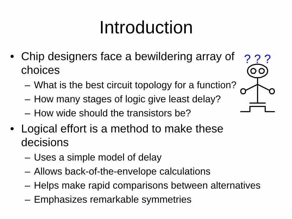
Introduction• Chip designers face a bewildering array of
choices– What is the best circuit topology for a function?– How many stages of logic give least delay?– How wide should the transistors be?
• Logical effort is a method to make these decisions– Uses a simple model of delay– Allows back-of-the-envelope calculations– Helps make rapid comparisons between alternatives– Emphasizes remarkable symmetries
? ? ?
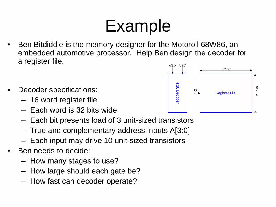
Example• Ben Bitdiddle is the memory designer for the Motoroil 68W86, an
embedded automotive processor. Help Ben design the decoder for a register file.
• Decoder specifications:– 16 word register file– Each word is 32 bits wide– Each bit presents load of 3 unit-sized transistors– True and complementary address inputs A[3:0]– Each input may drive 10 unit-sized transistors
• Ben needs to decide:– How many stages to use?– How large should each gate be?– How fast can decoder operate?
A[3:0] A[3:0]
16
32 bits
16 words
4:16 Decoder
Register File

Delay in a Logic Gate
• Express delays in process-independent unit
absddτ
=
τ = 3RC
≈ 12 ps in 180 nm process
40 ps in 0.6 μm process
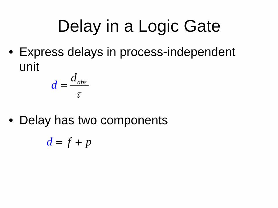
Delay in a Logic Gate• Express delays in process-independent
unit
• Delay has two components
absd dτ
=
d f p= +

Delay in a Logic Gate• Express delays in process-independent
unit
• Delay has two components
• Effort delay f = gh (a.k.a. stage effort)– Again has two components
absddτ
=
d pf= +

Delay in a Logic Gate• Express delays in process-independent unit
• Delay has two components
• Effort delay f = gh (a.k.a. stage effort)– Again has two components
• g: logical effort– Measures relative ability of gate to deliver current– g ≡ 1 for inverter
absddτ
=
d f p= +
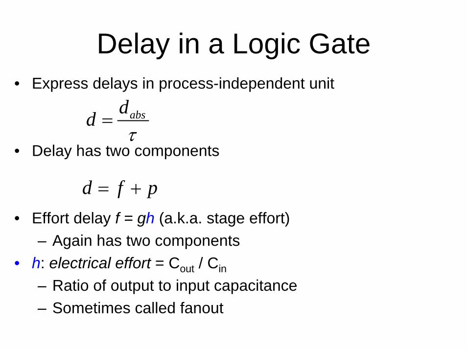
Delay in a Logic Gate• Express delays in process-independent unit
• Delay has two components
• Effort delay f = gh (a.k.a. stage effort)– Again has two components
• h: electrical effort = Cout / Cin
– Ratio of output to input capacitance– Sometimes called fanout
absddτ
=
d f p= +
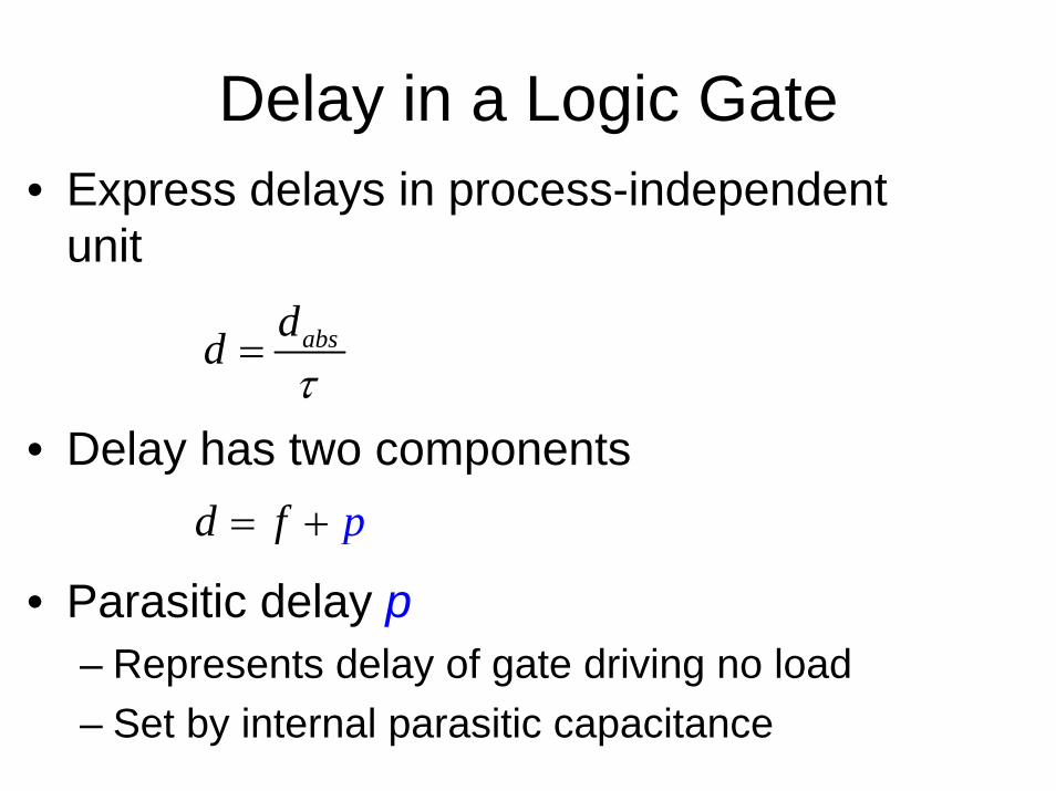
Delay in a Logic Gate• Express delays in process-independent
unit
• Delay has two components
• Parasitic delay p– Represents delay of gate driving no load– Set by internal parasitic capacitance
absddτ
=
d pf= +

Delay Plots
d = f + p= gh + p
Electrical Effort:h = Cout / Cin
Nor
mal
ized
Del
ay: d
Inverter2-inputNAND
g =p =d =
g =p =d =
0 1 2 3 4 5
0
1
2
3
4
5
6

Delay Plots
d = f + p= gh + p
• What about NOR2?
Electrical Effort:h = Cout / Cin
Nor
mal
ized
Del
ay: d
Inverter2-inputNAND
g = 1p = 1d = h + 1
g = 4/3p = 2d = (4/3)h + 2
Effort Delay: f
Parasitic Delay: p
0 1 2 3 4 5
0
1
2
3
4
5
6
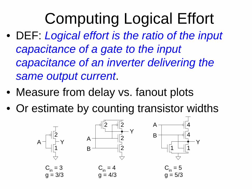
Computing Logical Effort• DEF: Logical effort is the ratio of the input
capacitance of a gate to the input capacitance of an inverter delivering the same output current.
• Measure from delay vs. fanout plots• Or estimate by counting transistor widths
A Y A
B
YA
BY
1
2
1 1
2 2
2
2
4
4
Cin = 3g = 3/3
Cin = 4g = 4/3
Cin = 5g = 5/3
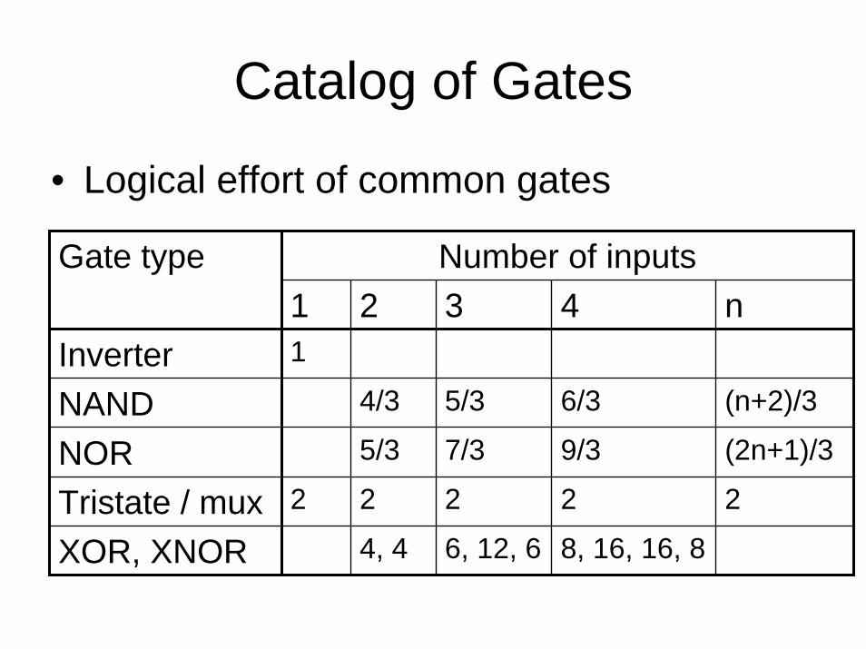
Catalog of Gates
Number of inputsGate type1 2 3 4 n
Inverter 1
NAND 4/3 5/3 6/3 (n+2)/3
NOR 5/3 7/3 9/3 (2n+1)/3
Tristate / mux 2 2 2 2 2
XOR, XNOR 4, 4 6, 12, 6 8, 16, 16, 8
• Logical effort of common gates
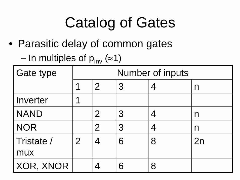
Catalog of Gates
Number of inputsGate type1 2 3 4 n
Inverter 1NAND 2 3 4 nNOR 2 3 4 nTristate / mux
2 4 6 8 2n
XOR, XNOR 4 6 8
• Parasitic delay of common gates– In multiples of pinv (≈1)

Example: Ring Oscillator• Estimate the frequency of an N-stage ring
oscillator
Logical Effort: g = Electrical Effort: h =Parasitic Delay: p =Stage Delay: d =Frequency: fosc =

Example: Ring Oscillator• Estimate the frequency of an N-stage ring
oscillator
Logical Effort: g = 1Electrical Effort: h = 1Parasitic Delay: p = 1Stage Delay: d = 2Frequency: fosc = 1/(2*N*d) = 1/4N
31 stage ring oscillator in 0.6 μm process has frequency of ~ 200 MHz
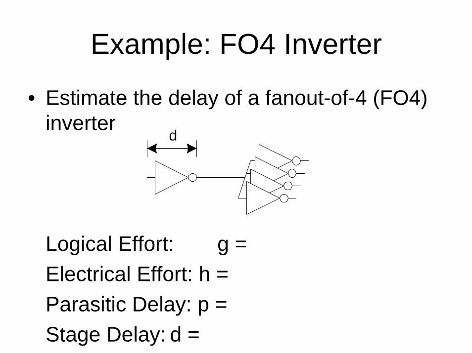
Example: FO4 Inverter
• Estimate the delay of a fanout-of-4 (FO4) inverter
Logical Effort: g = Electrical Effort: h =Parasitic Delay: p =Stage Delay: d =
d
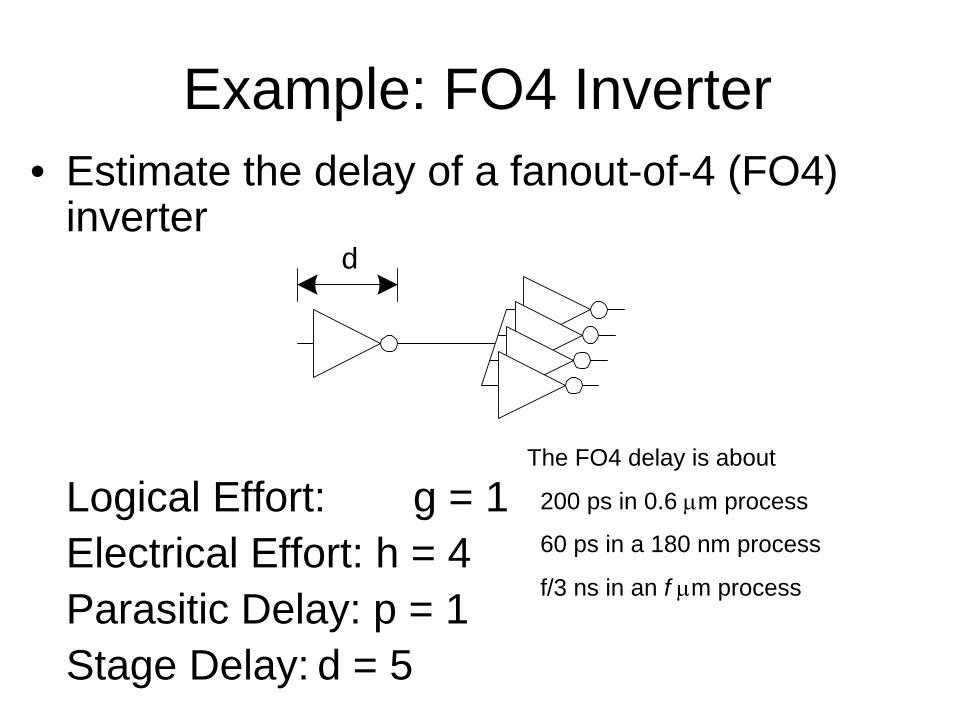
Example: FO4 Inverter• Estimate the delay of a fanout-of-4 (FO4)
inverter
Logical Effort: g = 1Electrical Effort: h = 4Parasitic Delay: p = 1Stage Delay: d = 5
d
The FO4 delay is about
200 ps in 0.6 μm process
60 ps in a 180 nm process
f/3 ns in an f μm process

References
• Adnan Aziz’s Logic Synthesis Course website
http://research.sun.com/vlsi/Publications/KPDisclosed/logeff/logeff.pdf
• Logical Effort, by Ivan Sutherland, Bob Sproull, and David Harris (Morgan Kaufmann, San Francisco, 1999)
Questions and Answers
Thank You


