23
Lecture 17 – Optical Lithography 2 - Optics EECS 598-002 Winter 2006 Nanophotonics and Nano-scale Fabrication P.C.Ku

Lecture 17 –Optical Lithography 2 - Optics
EECS 598-002 Winter 2006Nanophotonics and Nano-scale Fabrication
P.C.Ku
2EECS 598-002 Nanophotonics and Nanoscale Fabrication by P.C.Ku
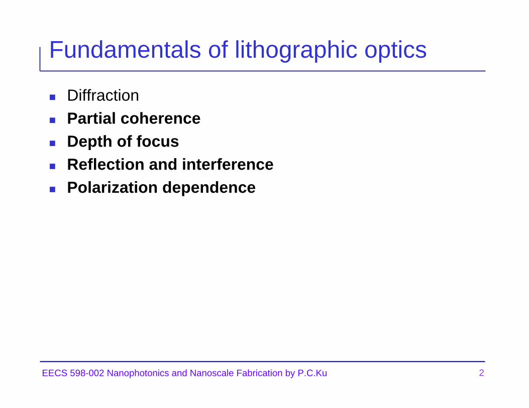
Fundamentals of lithographic optics
DiffractionPartial coherenceDepth of focusReflection and interferencePolarization dependence

3EECS 598-002 Nanophotonics and Nanoscale Fabrication by P.C.Ku
Image formation
Need to have at least the 0-th and the 1st diffraction orders being collected to recover the pitch information.
+1
-1
0
0
-1
Oblique incidence can improvethe minimum pitch but resultin a less image contrast.
Resolution limit (min pitch)= 2
2NA NAλ λ
× =

4EECS 598-002 Nanophotonics and Nanoscale Fabrication by P.C.Ku
Why not just use oblique incidence?
Because patterns on the mask are often random. Oblique illumination at a certain angle is only optimized for a specific structure (e.g. a line/space pattern at a certain pitch.)

5EECS 598-002 Nanophotonics and Nanoscale Fabrication by P.C.Ku
Incoherent illumination
0
-1
1
0
+1
-1
0
Some images may form.Some may not.
Resolution limit = 2NAλ

6EECS 598-002 Nanophotonics and Nanoscale Fabrication by P.C.Ku
Partial coherence
Illuminator Aperture
Entrance Pupil
Mask
Condenser
ab
optics)ion NA(projectator)NA(illumin
=≡abσ
7EECS 598-002 Nanophotonics and Nanoscale Fabrication by P.C.Ku
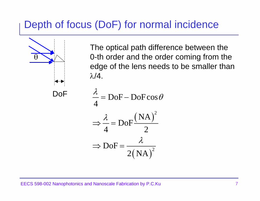
Depth of focus (DoF) for normal incidence
DoF
The optical path difference between the0-th order and the order coming from theedge of the lens needs to be smaller thanλ/4.
θ
( )
( )
2
2
DoF DoFcos4
NADoF
4 2
DoF2 NA
λ θ
λ
λ
= −
⇒ =
⇒ =

8EECS 598-002 Nanophotonics and Nanoscale Fabrication by P.C.Ku
DoF for oblique incidence
0
-1
θ
( ) ( )2 2sin cos sin cos
2 cos 22cos sin
i x z i x z
y
i z
E Ae Ae
Ae x
π πθ θ θ θλ λ
π θλ π θ
λ
+ − += +
⎛ ⎞= ⎜ ⎟⎝ ⎠
z
x
If equal amplitudes:
independent of z!DoF = ∞
9EECS 598-002 Nanophotonics and Nanoscale Fabrication by P.C.Ku
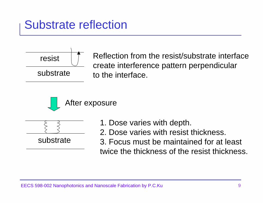
Substrate reflection
resist
substrate
Reflection from the resist/substrate interfacecreate interference pattern perpendicularto the interface.
substrate
After exposure
1. Dose varies with depth.2. Dose varies with resist thickness.3. Focus must be maintained for at leasttwice the thickness of the resist thickness.
10EECS 598-002 Nanophotonics and Nanoscale Fabrication by P.C.Ku
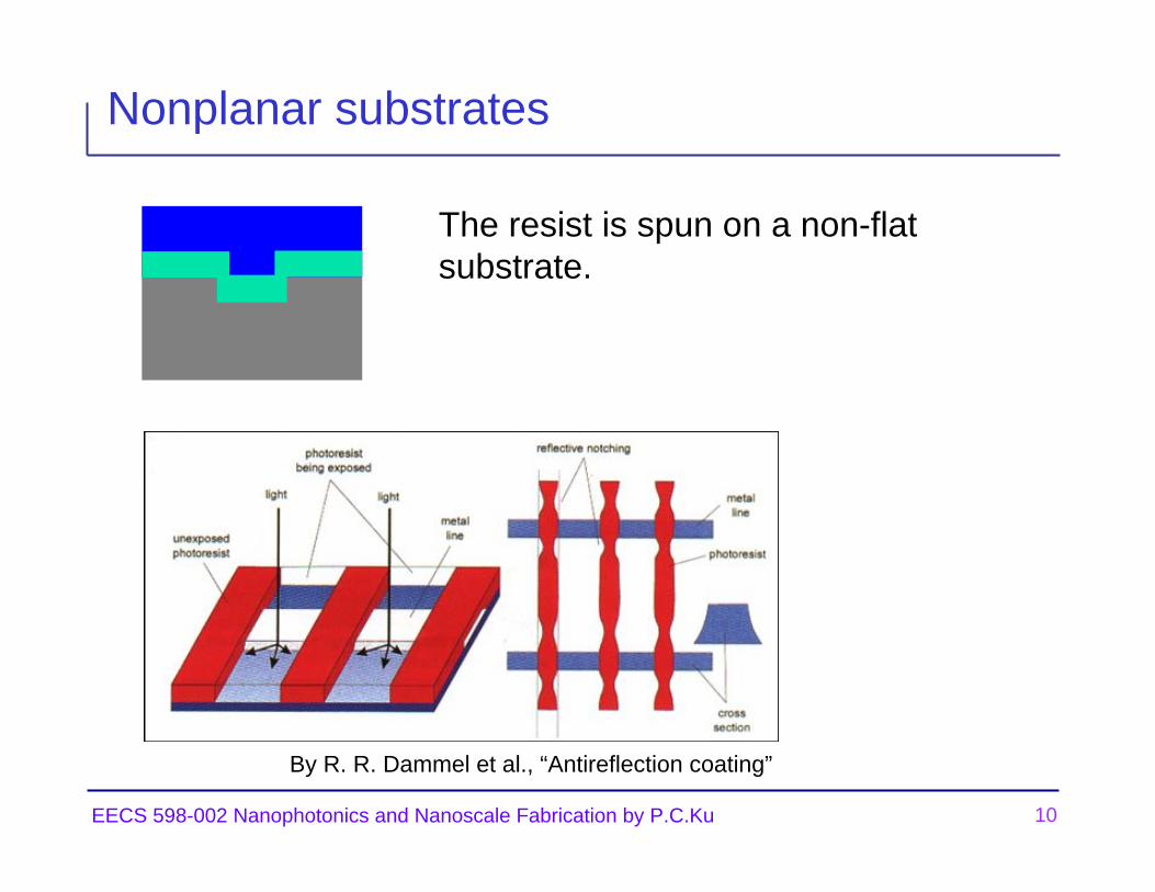
Nonplanar substrates
The resist is spun on a non-flat substrate.
By R. R. Dammel et al., “Antireflection coating”

11EECS 598-002 Nanophotonics and Nanoscale Fabrication by P.C.Ku
Swing curve vs wavelength
Typical substrates exhibit a larger reflectivity at a shorter wavelength.
By R. R. Dammel et al., “Antireflection coating”

12EECS 598-002 Nanophotonics and Nanoscale Fabrication by P.C.Ku
Minimize the reflectivity problems
Very minimum we can do:Post exposure bake (PEB) to induce the diffusion of the photo generated compound to smooth out the interference profile.
Antireflection layer (AR):Can be inorganic or organic materials.Can be on top of or underneath the resist.Typically good to absorb the light before it reaches the substrate
Examples:Si(ON) (hardmask) – a good mask for metal etchBARC (bottom AR coating) Can be spun on just like resist itselfTARC (top AR coating)
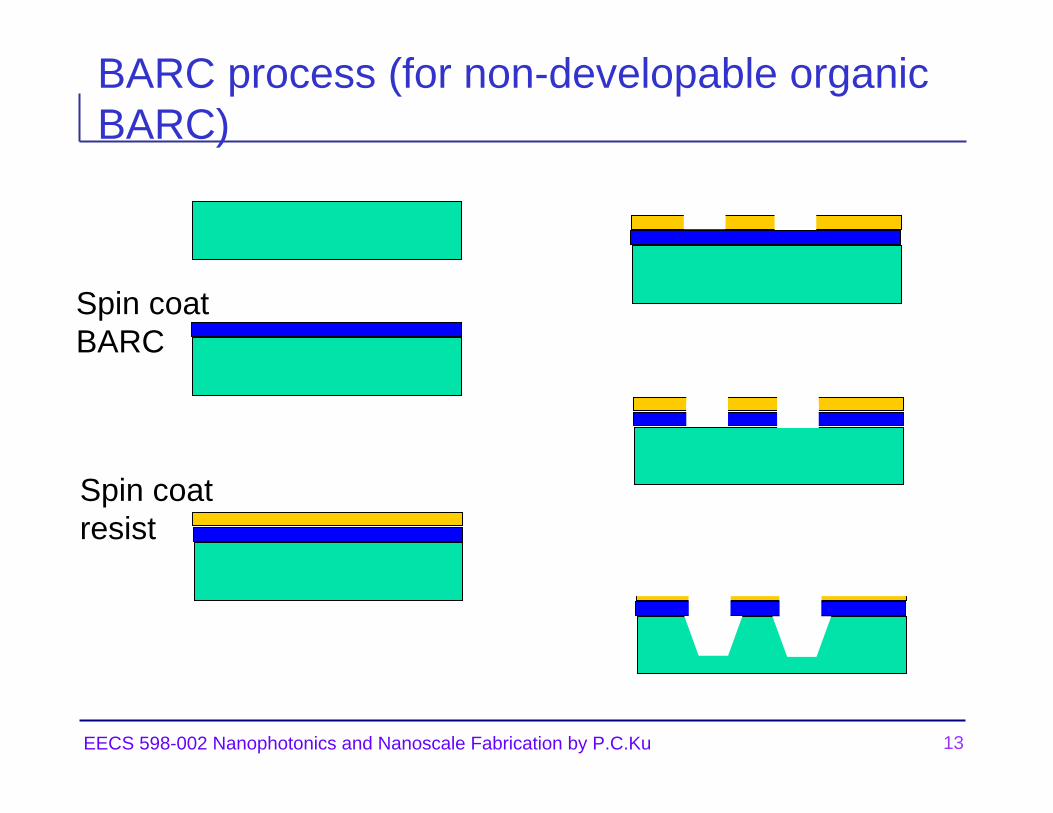
13EECS 598-002 Nanophotonics and Nanoscale Fabrication by P.C.Ku
BARC process (for non-developable organic BARC)
Spin coatBARC
Spin coatresist

14EECS 598-002 Nanophotonics and Nanoscale Fabrication by P.C.Ku
Advantages of organic BARC vs hardmask
Can be spin-coated. Can planarize the surface topologySome BARC’s can be developed at the same time as the resist. Save one etching step.BARC can be stripped at the same time with the resist while the hardmask can not be removed after it’s been deposited. This will improve the line yield.

15EECS 598-002 Nanophotonics and Nanoscale Fabrication by P.C.Ku
Polarization dependence
In general, the reflectivity of TE and TM components are different from each other.
As the feature size on the mask becomes comparable to the wavelength, a fully vectorial diffraction theory needs to be taken into account to accurately simulate the aerial image.

Mask

17EECS 598-002 Nanophotonics and Nanoscale Fabrication by P.C.Ku
Mask (reticle) design
pellicle
glass
chrome
Clear field Dark field
E-beam litho is typicallyused for mask making.

18EECS 598-002 Nanophotonics and Nanoscale Fabrication by P.C.Ku
Dose sensitivity
Comparison of clear and dark fields
1/3 intensitypasses throughdark field mask
Reaching reticle 20 mJ
Reaching wafer 15 mJ
60 mJ
15 mJ
24 mJ reach mask
18 mJ reach wfr
64 mJ reach mask
16 mJ reach wfr
Clear field Dark field
same variation of laser intensity
20% dose error for clear field6.7% dose error for dark field
19EECS 598-002 Nanophotonics and Nanoscale Fabrication by P.C.Ku
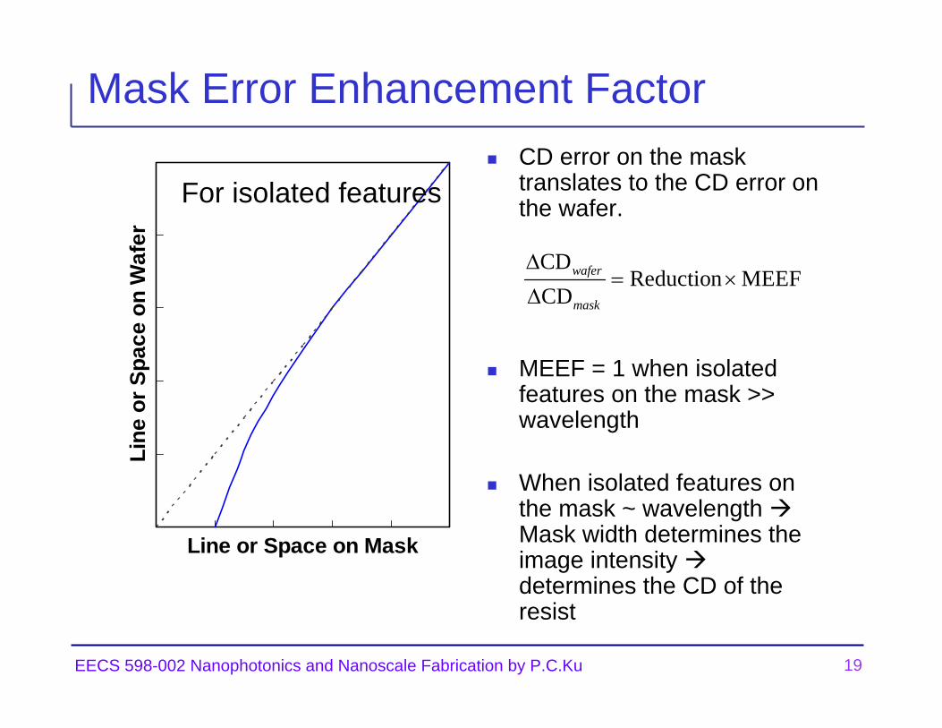
Mask Error Enhancement Factor
Line or Space on Mask
Line
or S
pace
on
Waf
erCD error on the mask translates to the CD error on the wafer.
MEEF = 1 when isolated features on the mask >> wavelength
When isolated features on the mask ~ wavelength Mask width determines the image intensity determines the CD of the resist
CDReduction MEEF
CDwafer
mask
∆= ×
∆
For isolated features
20EECS 598-002 Nanophotonics and Nanoscale Fabrication by P.C.Ku
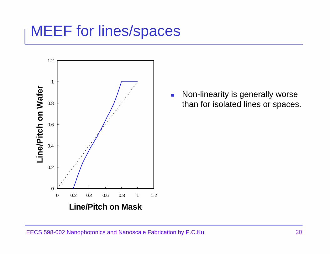
MEEF for lines/spaces
0
0.2
0.4
0.6
0.8
1
1.2
0 0.2 0.4 0.6 0.8 1 1.2
Line/Pitch on Mask
Line
/Pitc
h on
Waf
er Non-linearity is generally worse than for isolated lines or spaces.

Light source

22EECS 598-002 Nanophotonics and Nanoscale Fabrication by P.C.Ku
Overview
Exposure wavelengthG-line (436 nm)I-line (365 nm)KrF (248 nm)ArF (193 nm)F2 (157 nm)EUV (13.4 nm)X-ray (~ 1 nm)
Minimum feature size:~ 500 nm~ 350 nm~ 120 nm~ 70 nm ?
???
DUV

23EECS 598-002 Nanophotonics and Nanoscale Fabrication by P.C.Ku
Excimer lasers and dose control
Excimer laser is a pulsed laserRepetition rate ~ 1 kHz
Excimer laserND filter
Moving waferScanning speed< 100 mm/sec
Adjust ND filter OD setting and the scanning speed to control the exposuredose (mJ/cm2)


