LECTURE 170 – TEMPERATURE STABLE REFERENCESLECTURE ORGANIZATION
Outline• Principles of temperature stable references• Examples of temperature stable references• Design of bias voltages for a chip• SummaryCMOS Analog Circuit Design, 2nd Edition ReferencePages 153-159
Lecture 170 – Temperature Stable References (4/20/10) Page 170-2
PRINCIPLES OF TEMPERATURE STABLE REFERENCESTemperature Stable References• The previous reference circuits failed to provide small values of temperature coefficient
although sufficient power supply independence was achieved.• This section introduces a temperature stable reference that cancels a positive
temperature coefficient with a negative temperature coefficient. The technique issometimes called the bandgap reference although it has nothing to do with thebandgap voltage.
PrincipleVREF(T) = VPTAT(T) + K·VCTAT(T)
whereVPTAT(T) is a voltage that is proportionalto absolute temperature (PTAT)VCTAT(T) is a voltage that iscomplimentary to absolute temperature(CTAT)
andK is a temperature independent constant that makes VREF(T) independent oftemperature
Lecture 170 – Temperature Stable References (4/20/10) Page 170-3
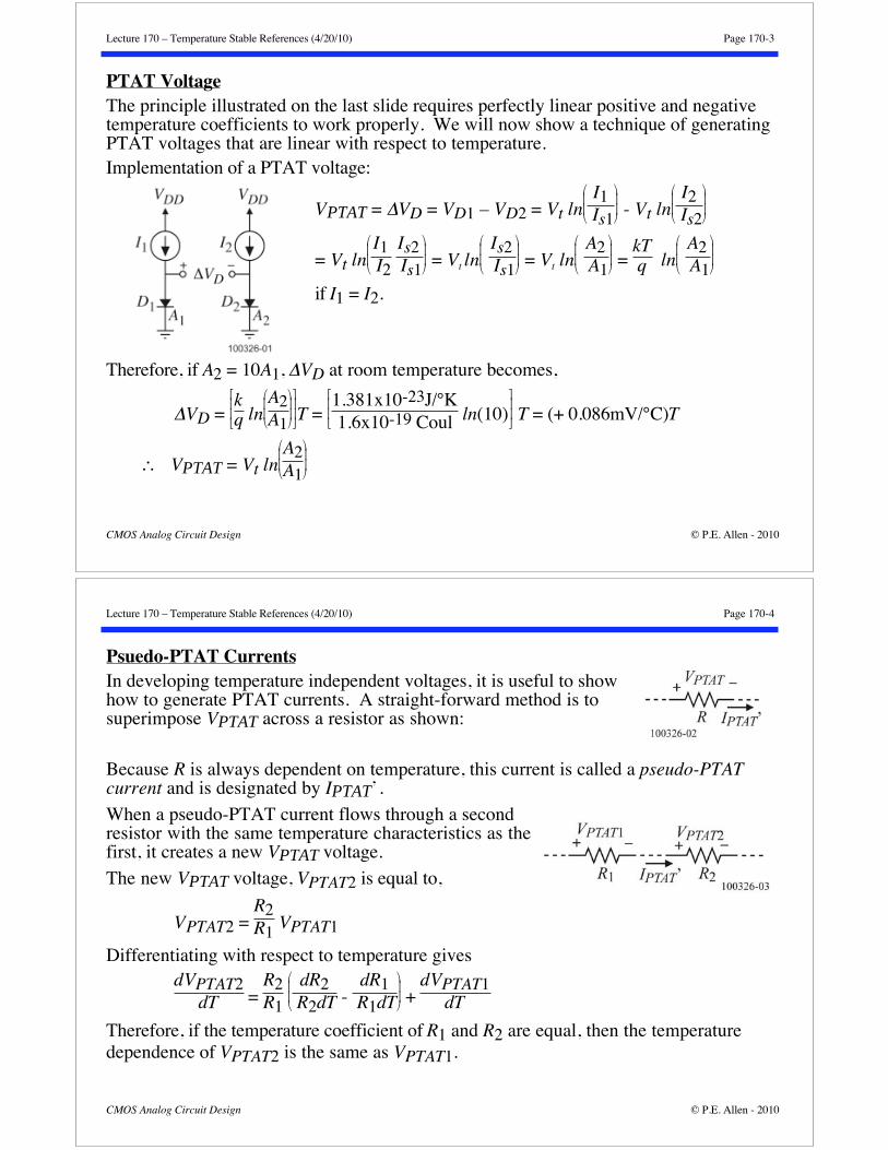
PTAT VoltageThe principle illustrated on the last slide requires perfectly linear positive and negativetemperature coefficients to work properly. We will now show a technique of generatingPTAT voltages that are linear with respect to temperature.Implementation of a PTAT voltage:
VPTAT = VD = VD1 – VD2 = Vt lnI1Is1 - Vt ln
I2Is2
= Vt lnI1I2
Is2Is1 = Vt ln
Is2Is1 = Vt ln
A2A1 =
kTq ln
A2A1
if I1 = I2.
Therefore, if A2 = 10A1, VD at room temperature becomes,
VD = kq ln
A2A1 T =
1.381x10⁻²³J/°K1.6x10-19 Coul ln(10) T = (+ 0.086mV/°C)T
VPTAT = Vt lnA2A1
Lecture 170 – Temperature Stable References (4/20/10) Page 170-4
Psuedo-PTAT CurrentsIn developing temperature independent voltages, it is useful to showhow to generate PTAT currents. A straight-forward method is tosuperimpose VPTAT across a resistor as shown:
Because R is always dependent on temperature, this current is called a pseudo-PTATcurrent and is designated by IPTAT’.
When a pseudo-PTAT current flows through a secondresistor with the same temperature characteristics as thefirst, it creates a new VPTAT voltage.
The new VPTAT voltage, VPTAT2 is equal to,
VPTAT2 = R2R1 VPTAT1
Differentiating with respect to temperature givesdVPTAT2
dT = R2R1
dR2R2dT -
dR1R1dT +
dVPTAT1dT
Therefore, if the temperature coefficient of R1 and R2 are equal, then the temperaturedependence of VPTAT2 is the same as VPTAT1.
Lecture 170 – Temperature Stable References (4/20/10) Page 170-5
Pseudo-PTAT Currents - ContinuedThis can be done through the circuits below which use only MOSFETs and pn junctionsor MOSFETs, an op amp and pn junctions.
In these circuits, I1 = I2 and the voltage across D1 is made equal to the voltage across theseries combination of R and D2 to create the pseudo-PTAT current,
IPTAT’ = VD1 - VD2
R = kTRq ln
A2A1
where VGS1 = VGS2 for the MOSFET only version.
Psuedo-PTAT current generator using
only MOSFETs and pn junctions.
VDD
I1
VDD
I2
+
−VGS1
D1D2A1 A2
Μ1 Μ2
Μ3Μ4
+
−VGS2
R IPTAT’
VDD
Μ5
IPTAT’
Psuedo-PTAT current generator using
MOSFETs, an op amp and pn junctions.
VDD
I1
VDD
I2
D1D2A1 A2
Μ1 Μ2 Μ3
R IPTAT’
VDD
IPTAT’+ −
100326-04
Lecture 170 – Temperature Stable References (4/20/10) Page 170-6
CTAT VoltageThis becomes more challenging because a true CTAT voltage does not exist. The bestapproach is to examine the pn junction (can be a diode or BJT).The current through a pn junction shown can be written as,
JD = qDnni2
LnNA+
qDppno
Lp
(vD VG0)Vt
= AT exp vD VG0
Vt
Consider the circuit shown. It can be shown, that vD(T) can be given as,
vD(T) = VGO 1 -TT0 + vD0
TT0 +
kTq ln
T0T +
kTq ln
JDJD0
where,VGO = bandgap voltage of silicon (1.205V)T0 = a reference temperature about which T varies
= a temperature coefficient for the pn junction saturation current ( 3)JD = pn junction current density
In the above expression for vD(T) the term kTq ln
T0
T is not linear with T!!
This term will create a problem called “bandgap curvature problem” because a perfectlylinear PTAT function cannot be cancelled by a term that is not truly CTAT.
Lecture 170 – Temperature Stable References (4/20/10) Page 170-7
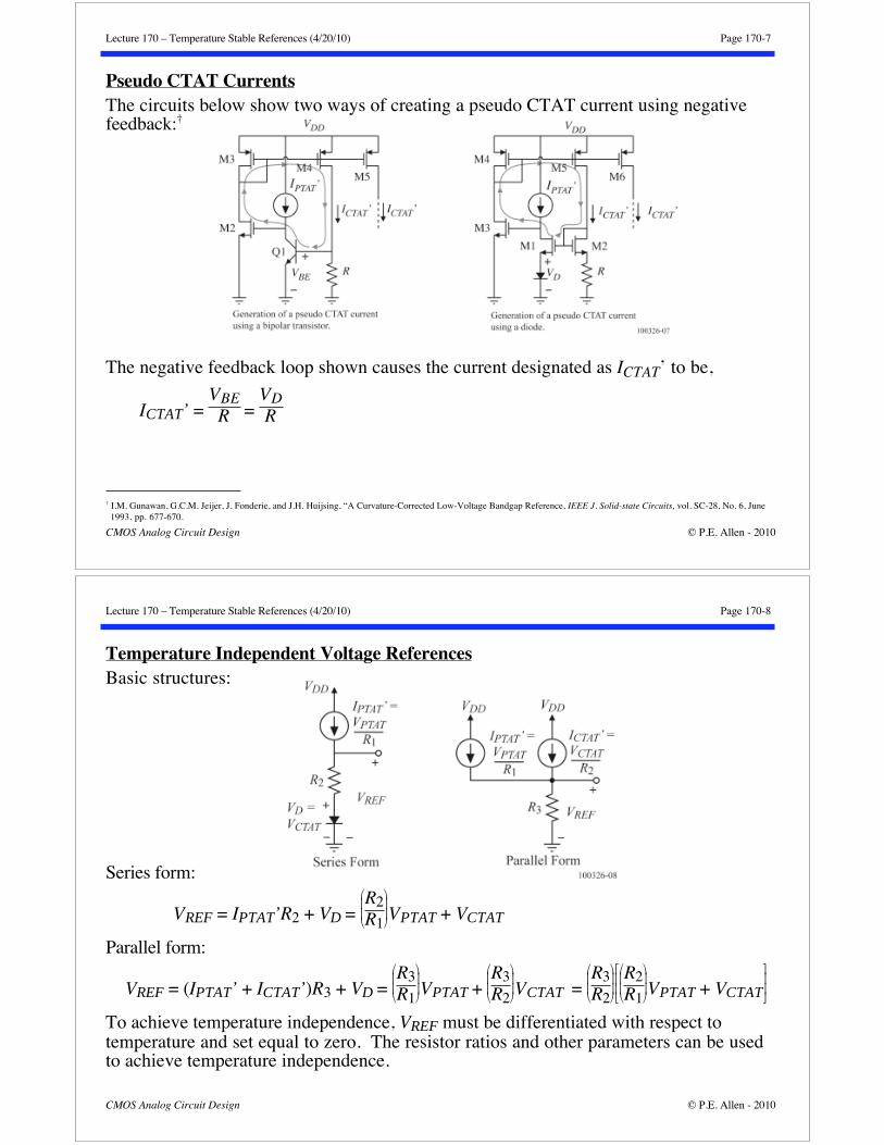
Temperature Independent Voltage ReferencesBasic structures:
Series form:
VREF = IPTAT’R2 + VD = R2R1
VPTAT + VCTAT
Parallel form:
VREF = (IPTAT’ + ICTAT’)R3 + VD = R3R1
VPTAT + R3R2
VCTAT = R3R2
R2R1
VPTAT + VCTAT
To achieve temperature independence, VREF must be differentiated with respect totemperature and set equal to zero. The resistor ratios and other parameters can be usedto achieve temperature independence.
Lecture 170 – Temperature Stable References (4/20/10) Page 170-9
Example 170-1 – Temp. Independent Constant for Series and Parallel References(a.) Design the ratio of R2/R1 for the series configuration if VCTAT = 0.6V and A2/A1 = 10for room temperature (Vt = 0.026V). Assume = 3.2 and = 1. Find the value of VREF.
R2R1 =
VGO - VCTAT + ( - )Vt0VPTAT =
1.205 - 0.6 + 2.2(0.026)0.026(2.3026) = 11.06
VREF = 1.205 + 2.2(0.026) = 1.262V(b.) For the parallel configuration find the values of R2/R1 and R3/R2 if VREF = 0.5V.
From (a.) we know that R2/R1 = 11.05. We also know that,
Example 170-2 – Design of the Previous Temperature Independent ReferenceAssume that AE1 = 10 AE2, VEB2 = 0.7 V, R2 = R3, and Vt = 0.026 V at room temperaturefor temperature independent reference on the previous slide. Find R2/R1 to give a zerotemperature coefficient at room temperature. If VOS = 10 mV, find the change in VREF. Notethat I1R2 = VREF VEB2 VOS.
Evaluating the temperature independent constant gives
R2R1
ln R2 AE1R3AE2
= VGO - VCTAT + ( - )Vt0
VPTAT =
1.205 - 0.7 + (2.2)(0.026)0.026 = 21.62
Therefore, R2/R1 = 9.39. In order to use the equation for VREF with VOS 0, we mustknow the approximate value of VREF and iterate if necessary because I1 is a function ofVREF. Assuming VREF to be 1.262, we obtain from
VREF = VEB2 - 1 +R2R1
VOS + R2R1
Vt lnR2AE1R1AE2
1 -VOS
VREF - VEB2 - VOS
a new value VREF = 1.153 V. The second iteration makes little difference on the resultbecause VREF is in the argument of the logarithm
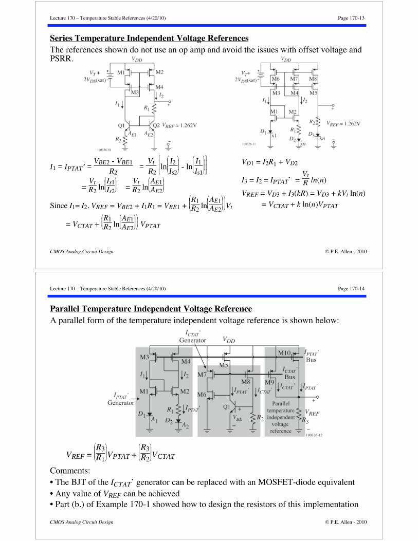
Lecture 170 – Temperature Stable References (4/20/10) Page 170-13
Parallel Temperature Independent Voltage ReferenceA parallel form of the temperature independent voltage reference is shown below:
VREF = R3R1
VPTAT + R3R2
VCTAT
Comments:• The BJT of the ICTAT’ generator can be replaced with an MOSFET-diode equivalent• Any value of VREF can be achieved• Part (b.) of Example 170-1 showed how to design the resistors of this implementation
Lecture 170 – Temperature Stable References (4/20/10) Page 170-15
How Can a Bandgap “Current” Reference be Obtained?Use a MOSFET under ZTC operation and design the parallel form of the bandgap voltagereference to give a value of VZTC.
060529-09
VDD
IPTAT
VDD
IVBE
R3+
−VREF =VGS(ZTC)
IREF
Lecture 170 – Temperature Stable References (4/20/10) Page 170-16
T term of the pnjunction contributed a nonlinearity to theCTAT realization. This is illustrated by thedashed lines in the plot shown.The result is shown below where the referencevoltage is not constant with temperature.
Comments:• True temperature independence is only achieved over a small range of temperatures• References that do not correct this problem have a temperature dependence of 10
ppm°/C to 50 ppm/°C over 0°C to 70°C.
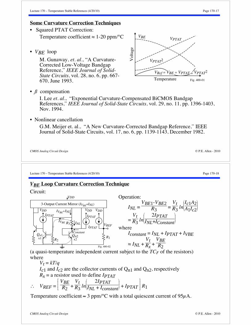
Lecture 170 – Temperature Stable References (4/20/10) Page 170-17
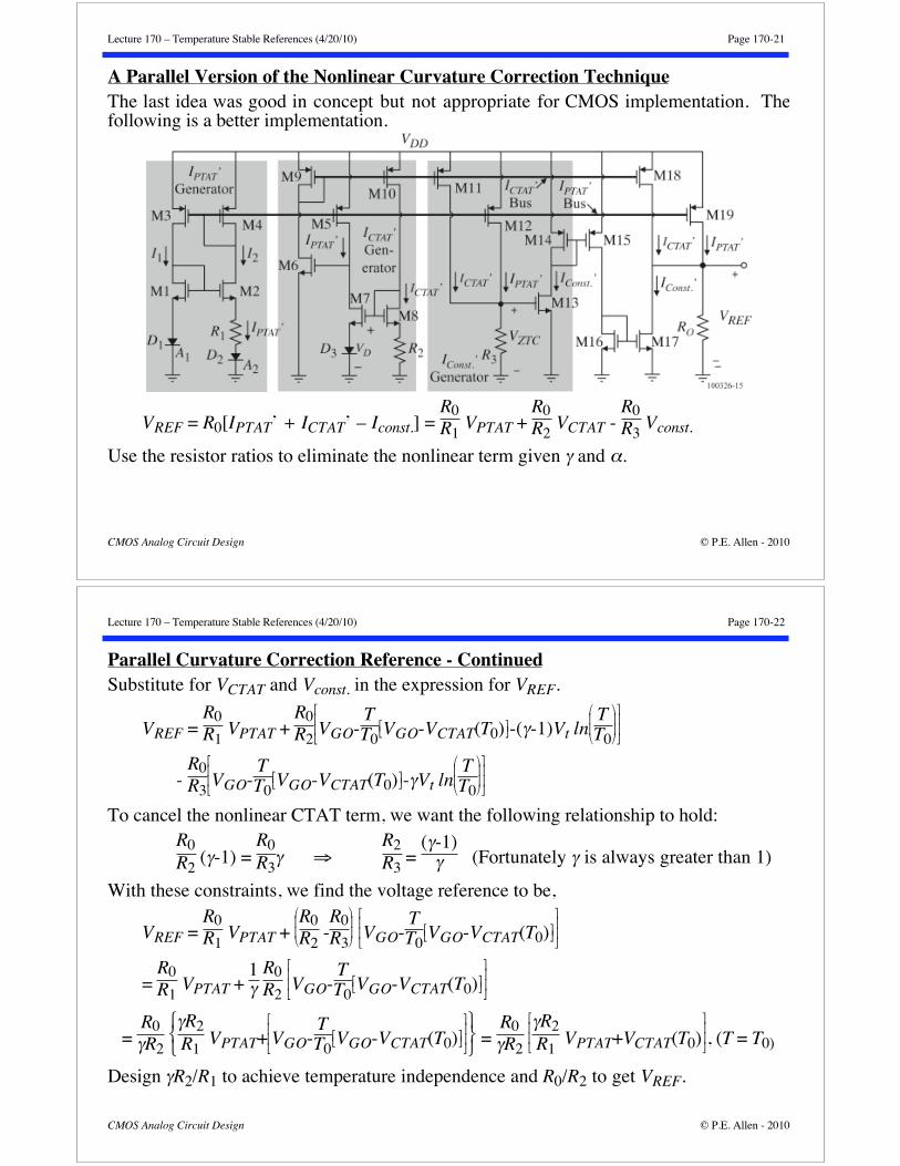
A Parallel Version of the Nonlinear Curvature Correction TechniqueThe last idea was good in concept but not appropriate for CMOS implementation. Thefollowing is a better implementation.
VREF = R0[IPTAT’ + ICTAT’ – Iconst.] = R0R1
VPTAT + R0R2
VCTAT - R0R3
Vconst.
Use the resistor ratios to eliminate the nonlinear term given and .
Lecture 170 – Temperature Stable References (4/20/10) Page 170-22
Example 170-3 – Design of a Zero Temperature Coefficient Voltage ReferenceAssume that VCTAT = 0.7 V, R3 = 10k , = 3.2, A2 = 10A1, and Vt = 0.026 V at room
temperature for the parallel curvature correction circuit. Find R2 and R3 to give a zerotemperature coefficient at room temperature and a reference voltage of 1.0V.
To eliminate the nonlinear CTAT term,R2R3
= ( -1)
= (2.2)3.2 = 0.6875 R2 = 6.88k
To cancel the temperature dependence,
Temp. independent constant = K = R2
R1=
VGO - VCTAT + ( - )Vt0VPTAT
orR2R1
= VGO - VCTAT + ( - )Vt0
VPTAT = (1.205 0.7 + (3.2-1)(0.026)
(0.026)(2.3026) = 9.3907 R1=2.34k
The reference voltage can be written as,
VREF = R0R2
R2R1
VPTAT+VCTAT(T0) = R0R2
[9.3907(0.026)(2.3026) + 0.7]
R0R2
= (3.2)1.262 = 2.535 R0 = 2.535R2 = 17.44k
Lecture 170 – Temperature Stable References (4/20/10) Page 170-24
DESIGN OF BIAS VOLTAGES FOR A CHIPDistributing Bias Voltages over a DistanceThe major problem is the IR drops in busses. For example,
100µA
100µA
1mm
M1 M2VBias
050716-01
ID1 ID2100µA
If the bus metal is 50m /sq. and is 5μm wide, the resistance of the bus in one direction is(50m /sq.)x(1000μm/5μm) = 10 . The difference in drain currents for an overdrive of0.1V is,
VGS1 = 1mV + VGS2 + 1mV = VGS2 + 2mV
ID1ID2 =
(VGS1-VTN)2
(VGS2-VTN)2 = (VGS2-VTN+2mV)2
(VGS2-VTN)2 = 0.1+0.002
0.12= 1.04
Lecture 170 – Temperature Stable References (4/20/10) Page 170-27
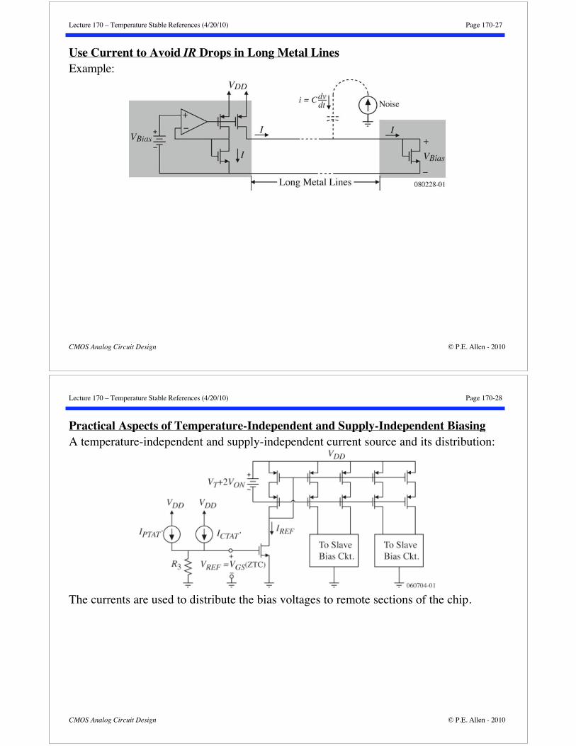
Practical Aspects of Temperature-Independent and Supply-Independent BiasingA temperature-independent and supply-independent current source and its distribution:
The currents are used to distribute the bias voltages to remote sections of the chip.
Lecture 170 – Temperature Stable References (4/20/10) Page 170-29
SUMMARY OF TEMPERATURE STABLE REFERENCES• The classical form of the temperature stable reference has a value of voltage close to the
bandgap voltage and is called the “bandgap voltage reference”.• Bandgap voltage references can achieve temperature dependence less than 50 ppm/°C• Correction of second-order effects in the bandgap voltage reference can achieve very
stable (1 ppm/°C) voltage references.• Watch out for second-order effects such as noise when using the bandgap voltage
reference in sensitive applications.• Distribution of bias voltages over a long distance should be done by current rather than


![100420 Final TGP Summary Report[1]](https://static.documents.pub/doc/80x56/577d37321a28ab3a6b950f95/100420-final-tgp-summary-report1.jpg)


