+ All Categories
Home > Documents > LECTURE 194 – CMOS PASSIVE COMPONENTS - IIpallen.ece.gatech.edu/.../L194-CMOSPassCompII(2... ·...

LECTURE 194 – CMOS PASSIVE COMPONENTS - IIpallen.ece.gatech.edu/.../L194-CMOSPassCompII(2... ·...

Date post: 18-Apr-2018
Category:
Upload: nguyenkhanh
View: 229 times
Download: 3 times
Share this document with a friend
12
Lecture 194 – CMOS Passive Components - II (7/10/02) Page 194-1 ECE 4430 - Analog Integrated Circuit Design I © P.E. Allen - 2002 LECTURE 194 – CMOS PASSIVE COMPONENTS - II (READING: Text-Sec. 2.10) Objective The objective of this presentation is: 1.) Examine the passive components that are compatible with CMOS technology 2.) Physical influence on passive components Outline Capacitors Resistors Summary Lecture 194 – CMOS Passive Components - II (7/10/02) Page 194-2 ECE 4430 - Analog Integrated Circuit Design I © P.E. Allen - 2002 Capacitor Errors 1.) Oxide gradients 2.) Edge effects 3.) Parasitics 4.) Voltage dependence 5.) Temperature dependence
Transcript

Lecture 194 – CMOS Passive Components - II (7/10/02) Page 194-1

ECE 4430 - Analog Integrated Circuit Design I © P.E. Allen - 2002

LECTURE 194 – CMOS PASSIVE COMPONENTS - II(READING: Text-Sec. 2.10)

ObjectiveThe objective of this presentation is:1.) Examine the passive components that are compatible with CMOS technology2.) Physical influence on passive componentsOutline• Capacitors• Resistors• Summary

Lecture 194 – CMOS Passive Components - II (7/10/02) Page 194-2

ECE 4430 - Analog Integrated Circuit Design I © P.E. Allen - 2002

Capacitor Errors1.) Oxide gradients2.) Edge effects3.) Parasitics4.) Voltage dependence5.) Temperature dependence

Lecture 194 – CMOS Passive Components - II (7/10/02) Page 194-3

ECE 4430 - Analog Integrated Circuit Design I © P.E. Allen - 2002

Capacitor Errors - Oxide GradientsError due to a variation in oxide thickness across the wafer.

Fig. 192-01

A1 A2 B

A1 B A2

(a)

(b)

x1 x2 x3

y

No commoncentroid layout

Common centroidlayout

Only good for one-dimensional errors.An alternate approach is to layout numerous repetitions and connect them randomly toachieve a statistical error balanced over the entire area of interest.

A B C

A

A

B

B

C

C

A B C

A

A

B

B

C

C

A B C

A

A

B

B

C

C

Fig. 194-02

0.2% matching of poly resistors was achieved using an array of 50 unit resistors.

Lecture 194 – CMOS Passive Components - II (7/10/02) Page 194-4

ECE 4430 - Analog Integrated Circuit Design I © P.E. Allen - 2002

Capacitor Errors - Edge EffectsThere will always be a randomness on the definition of the edge.However, etching can be influenced by the presence of adjacent structures.For example,

A BC

A BC

Matching of A and B are disturbed by the presence of C.

Improved matching achieved by balancing the adjacent material.

Fig. 194-03

Lecture 194 – CMOS Passive Components - II (7/10/02) Page 194-5

ECE 4430 - Analog Integrated Circuit Design I © P.E. Allen - 2002

Capacitor Errors - Area/Periphery RatioThe best match between two structures occurs when their area-to-periphery ratios areidentical.Let C’1 = C1 ± ∆C1 and C’2 = C2 ± ∆C2

whereC’ = the actual capacitanceC = the desired capacitance (which is proportional to area)∆C = edge uncertainty (which is proportional to the periphery)

Solve for the ratio of C’2/C’1,

C’2C’1

= C2 ± ∆C2C1 ± ∆C1

= C2C1

1 ± ∆C2C2

1 ± ∆C1C1

≈ C2C1

1 ± ∆C2C2

1 -+ ∆C1C1

≈ C2C1

1 ± ∆C2C2

-+ ∆C1C1

If ∆C2C2

= ∆C1C1

, then C’2C’1

= C2C1

Therefore, the best matching results are obtained when the area/periphery ratio of C2 isequal to the area/periphery ratio of C1.

Lecture 194 – CMOS Passive Components - II (7/10/02) Page 194-6

ECE 4430 - Analog Integrated Circuit Design I © P.E. Allen - 2002

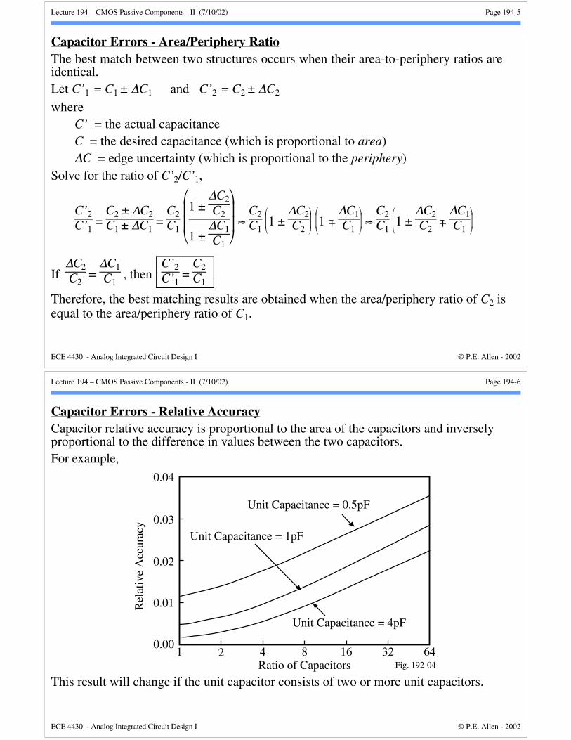
Capacitor Errors - Relative AccuracyCapacitor relative accuracy is proportional to the area of the capacitors and inverselyproportional to the difference in values between the two capacitors.For example,

0.04

0.03

0.02

0.01

0.001 2 4 8 16 32 64

Unit Capacitance = 0.5pF

Unit Capacitance = 1pF

Unit Capacitance = 4pF

Rel

ativ

e A

ccur

acy

Ratio of Capacitors Fig. 192-04

This result will change if the unit capacitor consists of two or more unit capacitors.

Lecture 194 – CMOS Passive Components - II (7/10/02) Page 194-7

ECE 4430 - Analog Integrated Circuit Design I © P.E. Allen - 2002

Capacitor Errors - ParasiticsParasitics are normally from the top and bottom plate to ac ground which is typically thesubstrate.

Top Plate

DesiredCapacitor

Topplate

parasitic

Bottom Plate

Bottomplate

parasiticFig. 194-05

Top plate parasitic is 0.01 to 0.001 of Cdesired

Bottom plate parasitic is 0.05 to 0.2 Cdesired

Lecture 194 – CMOS Passive Components - II (7/10/02) Page 194-8

ECE 4430 - Analog Integrated Circuit Design I © P.E. Allen - 2002

Other Considerations on Capacitor AccuracyDecreasing Sensitivity to Edge Variation:

A A'

B B'

A A'

B B'

Sensitive to edge variation in both upper andlower plates

Sensitive to edge varation inupper plate only. Fig. 194-06

A structure that minimizes the ratio of perimeter to area (circle is best).

Top Plateof Capacitor

Fig. 194-07

Bottom plateof capacitor

Lecture 194 – CMOS Passive Components - II (7/10/02) Page 194-9

ECE 4430 - Analog Integrated Circuit Design I © P.E. Allen - 2002

Capacitor Errors - Temperature and Voltage Dependence

Polysilicon-Oxide-Semiconductor CapacitorsAbsolute accuracy ≈ ±10%Relative accuracy ≈ ±0.2%Temperature coefficient ≈ +25 ppm/C°Voltage coefficient ≈ -50ppm/V

Polysilicon-Oxide-Polysilicon CapacitorsAbsolute accuracy ≈ ±10%Relative accuracy ≈ ±0.2%Temperature coefficient ≈ +25 ppm/C°Voltage coefficient ≈ -20ppm/V

Accuracies depend upon the size of the capacitors.

Accuracy ∝ 1/(Area2)

Lecture 194 – CMOS Passive Components - II (7/10/02) Page 194-10

ECE 4430 - Analog Integrated Circuit Design I © P.E. Allen - 2002

RESISTORSMOS Resistors - Source/Drain Resistor

p- substrate

FOX FOX

SiO2

Metal

n- well

p+

Fig. 194-08

Diffusion:10-100 ohms/squareAbsolute accuracy = ±35%Relative accuracy = 2% (5µm), 0.2% (50µm)Temperature coefficient = +1500 ppm/°CVoltage coefficient ≈ 200 ppm/V

Ion Implanted:500-2000 ohms/squareAbsolute accuracy = ±15%Relative accuracy = 2% (5µm), 0.15%(50 µm)Temperature coefficient = +400 ppm/°CVoltage coefficient ≈ 800 ppm/V

Comments:• Parasitic capacitance to substrate is voltage dependent.• Piezoresistance effects occur due to chip strain from mounting.

Lecture 194 – CMOS Passive Components - II (7/10/02) Page 194-11

ECE 4430 - Analog Integrated Circuit Design I © P.E. Allen - 2002

Polysilicon Resistor

Fig. 194-09

p- substrate

FOX

Polysilicon resistorMetal

30-100 ohms/square (unshielded)100-500 ohms/square (shielded)Absolute accuracy = ±30%Relative accuracy = 2% (5 µm)Temperature coefficient = 500-1000 ppm/°CVoltage coefficient ≈ 100 ppm/VComments:• Used for fuzes and laser trimming• Good general resistor with low parasitics

Lecture 194 – CMOS Passive Components - II (7/10/02) Page 194-12

ECE 4430 - Analog Integrated Circuit Design I © P.E. Allen - 2002

N-well Resistor

Fig. 194-10

p- substrate

FOX FOX

Metal

n- well

n+

FOX

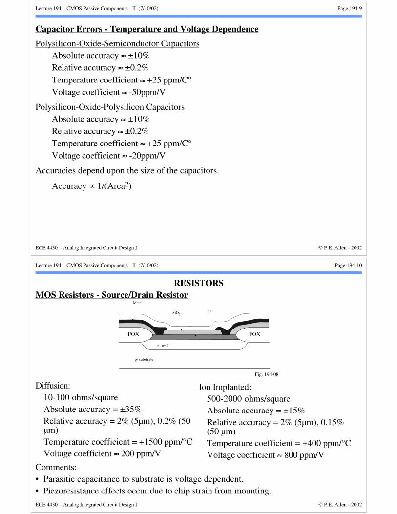
1000-5000 ohms/squareAbsolute accuracy = ±40%Relative accuracy ≈ 5%Temperature coefficient = 4000 ppm/°CVoltage coefficient is large ≈ 8000 ppm/VComments:• Good when large values of resistance are needed.• Parasitics are large and resistance is voltage dependent

Lecture 194 – CMOS Passive Components - II (7/10/02) Page 194-13

ECE 4430 - Analog Integrated Circuit Design I © P.E. Allen - 2002

MOS Passive Component Performance Summary

ComponentType

Range ofValues

AbsoluteAccuracy

RelativeAccuracy

TemperatureCoefficient

VoltageCoefficient

Poly-oxide-semiconductorCapacitor

0.35-0.5fF/µm2

10% 0.1% 20ppm/°C ±20ppm/V

Poly-PolyCapacitor

0.3-0.4 fF/µm2 20% 0.1% 25ppm/°C ±50ppm/V

DiffusedResistor

10-100 Ω/sq. 35% 2% 1500ppm/°C 200ppm/V

Ion ImplantedResistor

0.5-2 kΩ/sq. 15% 2% 400ppm/°C 800ppm/V

Poly Resistor 30-200 Ω/sq. 30% 2% 1500ppm/°C 100ppm/V

n-well Resistor 1-10 kΩ/sq. 40% 5% 8000ppm/°C 10kppm/V

The electrical performance of all passive components greatly depends on the geometryand physical aspects of the layout.

Lecture 194 – CMOS Passive Components - II (7/10/02) Page 194-14

ECE 4430 - Analog Integrated Circuit Design I © P.E. Allen - 2002

INDUCTORSInductorsWhat is the range of values for on-chip inductors?

0 10 20 30 40 50

12

10

8

6

4

2

0Frequency (GHz)

Indu

ctan

ce (

nH)

ωL = 50Ω

Inductor area is too large

Interconnect parasiticsare too large

Fig. 6-5

Consider an inductor used to resonate with 5pF at 1000MHz.

L = 1

4π2fo2C =

1(2π·109)2·5x10-12 = 5nH

Note: Off-chip connections will result in inductance as well.

Lecture 194 – CMOS Passive Components - II (7/10/02) Page 194-15

ECE 4430 - Analog Integrated Circuit Design I © P.E. Allen - 2002

Candidates for inductors in CMOS technology are:1.) Bond wires2.) Spiral inductors3.) Multi-level spiral4.) Solenoid

Bond wire Inductors:

β β

d Fig.6-6

• Function of the pad distance d and the bond angle β• Typical value is 1nH/mm which gives 2nH to 5nH in typical packages• Series loss is 0.2 Ω/mm for 1 mil diameter aluminum wire• Q ≈ 60 at 2 GHz

Lecture 194 – CMOS Passive Components - II (7/10/02) Page 194-16

ECE 4430 - Analog Integrated Circuit Design I © P.E. Allen - 2002

Planar Spiral InductorsSpiral Inductors on a Lossy Substrate:

C1

L R

C2

R2R1

Fig. 16-7

• Design Parameters:Inductance,L = Σ(Lself + Lmutual)

Quality factor, Q = ωLR

Self-resonant frequency: fself = 1LC

• Trade-off exists between the Q and self-resonant frequency• Typical values are L = 1-8nH and Q = 3-6 at 2GHz

Lecture 194 – CMOS Passive Components - II (7/10/02) Page 194-17

ECE 4430 - Analog Integrated Circuit Design I © P.E. Allen - 2002

Planar Spiral Inductors - ContinuedInductor Design

I

I

I

I

W

S

ID

Nturns = 2.5

SiO2

Silicon

Fig. 6-9

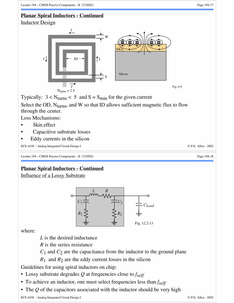
Typically: 3 < Nturns < 5 and S = Smin for the given current

Select the OD, Nturns, and W so that ID allows sufficient magnetic flux to flowthrough the center.Loss Mechanisms:• Skin effect• Capacitive substrate losses• Eddy currents in the silicon

Lecture 194 – CMOS Passive Components - II (7/10/02) Page 194-18

ECE 4430 - Analog Integrated Circuit Design I © P.E. Allen - 2002

Planar Spiral Inductors - ContinuedInfluence of a Lossy Substrate

C1

L R

C2

R2R1

Fig. 12.2-13

CLoad

where:L is the desired inductanceR is the series resistanceC1 and C2 are the capacitance from the inductor to the ground plane

R1 and R2 are the eddy current losses in the silicon

Guidelines for using spiral inductors on chip:• Lossy substrate degrades Q at frequencies close to fself• To achieve an inductor, one must select frequencies less than fself• The Q of the capacitors associated with the inductor should be very high

Lecture 194 – CMOS Passive Components - II (7/10/02) Page 194-19

ECE 4430 - Analog Integrated Circuit Design I © P.E. Allen - 2002

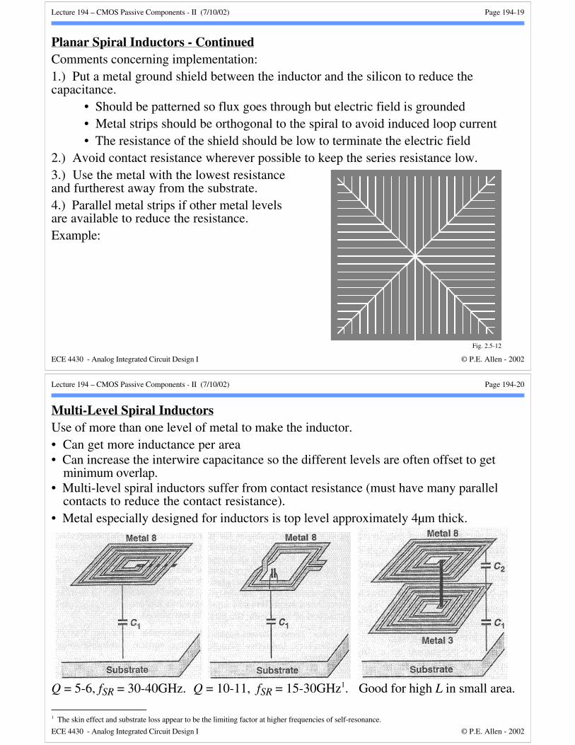
Planar Spiral Inductors - ContinuedComments concerning implementation:1.) Put a metal ground shield between the inductor and the silicon to reduce thecapacitance.

• Should be patterned so flux goes through but electric field is grounded• Metal strips should be orthogonal to the spiral to avoid induced loop current• The resistance of the shield should be low to terminate the electric field

2.) Avoid contact resistance wherever possible to keep the series resistance low.3.) Use the metal with the lowest resistanceand furtherest away from the substrate.4.) Parallel metal strips if other metal levelsare available to reduce the resistance.Example:

Fig. 2.5-12

Lecture 194 – CMOS Passive Components - II (7/10/02) Page 194-20

ECE 4430 - Analog Integrated Circuit Design I © P.E. Allen - 2002

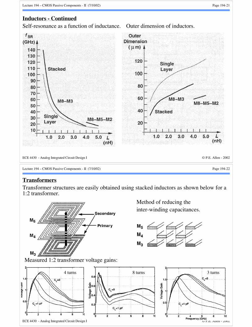
Multi-Level Spiral InductorsUse of more than one level of metal to make the inductor.• Can get more inductance per area• Can increase the interwire capacitance so the different levels are often offset to get

minimum overlap.• Multi-level spiral inductors suffer from contact resistance (must have many parallel

contacts to reduce the contact resistance).• Metal especially designed for inductors is top level approximately 4µm thick.

Q = 5-6, fSR = 30-40GHz. Q = 10-11, fSR = 15-30GHz1. Good for high L in small area.

1 The skin effect and substrate loss appear to be the limiting factor at higher frequencies of self-resonance.

Lecture 194 – CMOS Passive Components - II (7/10/02) Page 194-21

ECE 4430 - Analog Integrated Circuit Design I © P.E. Allen - 2002

Inductors - ContinuedSelf-resonance as a function of inductance. Outer dimension of inductors.

Lecture 194 – CMOS Passive Components - II (7/10/02) Page 194-22

ECE 4430 - Analog Integrated Circuit Design I © P.E. Allen - 2002

TransformersTransformer structures are easily obtained using stacked inductors as shown below for a1:2 transformer.

Method of reducing theinter-winding capacitances.

4 turns 8 turns 3 turns

Measured 1:2 transformer voltage gains:

Lecture 194 – CMOS Passive Components - II (7/10/02) Page 194-23

ECE 4430 - Analog Integrated Circuit Design I © P.E. Allen - 2002

Transformers – ContinuedA 1:4 transformer:Structure- Measured voltage gain-

Secondary

Lecture 194 – CMOS Passive Components - II (7/10/02) Page 194-24

ECE 4430 - Analog Integrated Circuit Design I © P.E. Allen - 2002

SUMMARY• IC passive components consist of:

Capacitors – depletion and parallel-plateResistors – diffusion/implantation, polysilicon, well/epitaxial and diodesInductors – metal spiral good at only high frequenciesTransformers – coupling coefficients of about 0.5-0.7

• For analog IC design, good quality passive components are extremely important• Passive components determine gains, time constants, current-to-voltage conversion,

etc.• Most technologies are driven by digital demands and passive components are highly

variable and have poor accuracies• Accuracy generally increases with area• Because IC technology has good relative accuracies for passive components, the

designer should always try to express the desired performance as ratios of similarpassive components.


Recommended