51
Lecture 2 – Analog circuits Seeing the light ….. I t
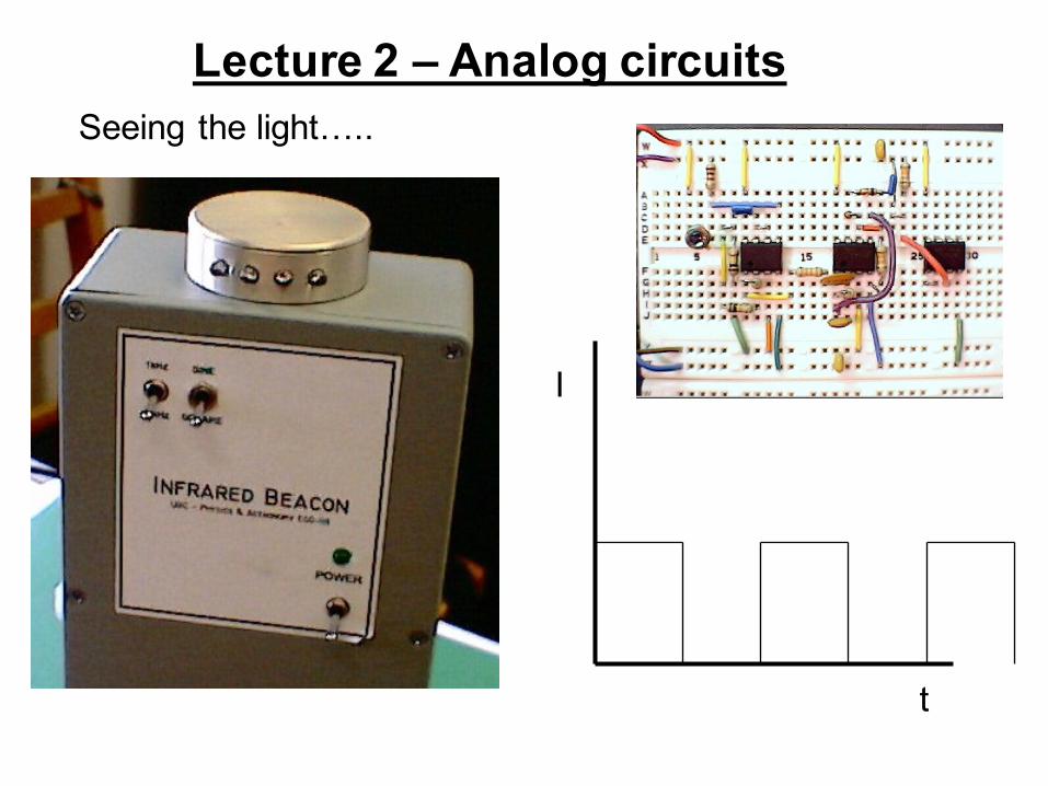
Lecture 2 – Analog circuitsSeeing the light…..
I
t

IR detection
IR light
Vout
t
Noise sources:• Electrical (60Hz, 120Hz, 180Hz….)• Other electrical• IR from lights• IR from cameras (autofocus)• Visible light
~ mV
Q1OP805
Vout
+V
V19V
RL
What we want: 0 – 5 V DC signal representing the IR amplitude.

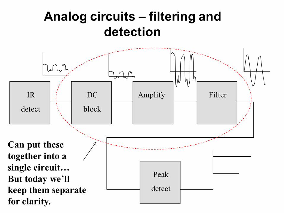
Analog circuits – filtering and detection
IR
detect
DC
block
Amplify Filter
Peak
detect
Analog circuits – filtering and detection
IR
detect
DC
block
Amplify Filter
Peak
detect
Can put these together into a single circuit…But today we’ll keep them separate for clarity.

Analog circuits – filtering and detection
IR
detect
DC
block
Amplify Filter
Peak
detect

6
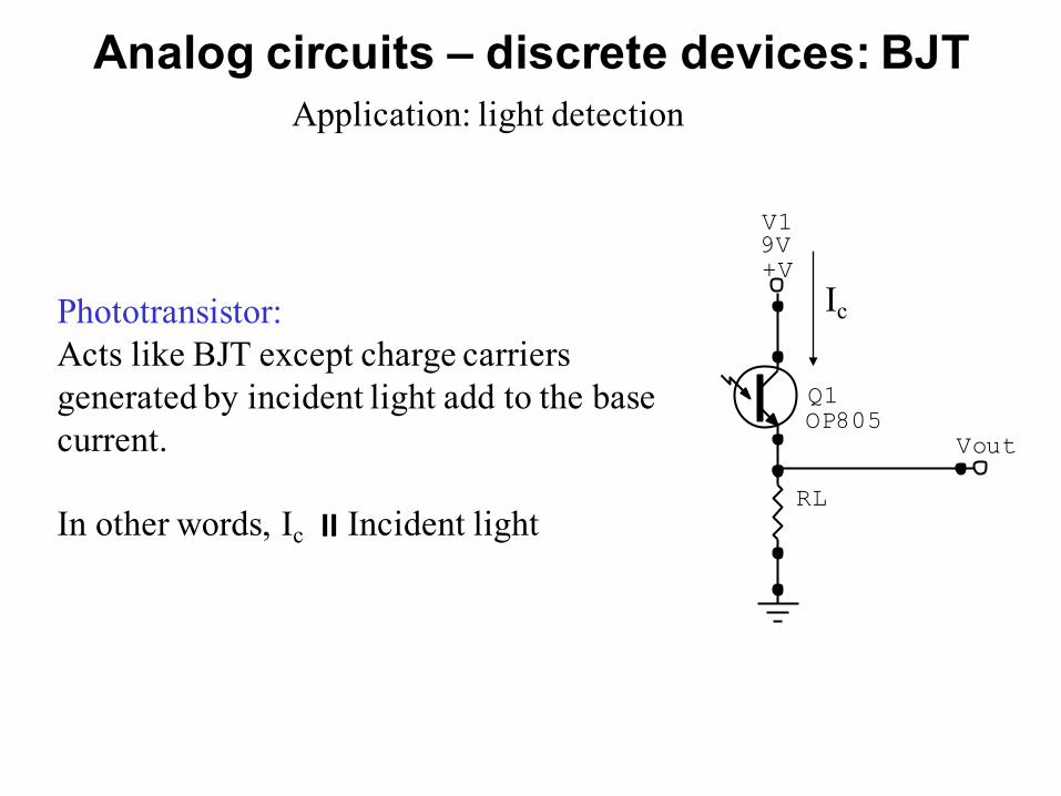
Discrete devices: BJT
Diagrams courtesy of: University of St. Andrews, St Andrews, Fife KY16 9SS, Scotland
Bipolar Junction Transistors
b ~ 20 - 100 or more
+
Q1OP805
Vout
+V
V19V
RL
Analog circuits – discrete devices: BJTApplication: light detection
Phototransistor:Acts like BJT except charge carriers generated by incident light add to the base current.
In other words, Ic ;Incident light
Ic

IR detection
Build a circuit that:
• Uses an OP805 and a resistor to detect variations in light with a voltmeter.
• Determine whether increasing or decreasing the load resistance makes it more sensitive
v Note: OP805 will see some room light – use your hand to block it, and use the voltmeter to detect the change in signal.

Vout = Ic * RL
+
Selecting RL ….
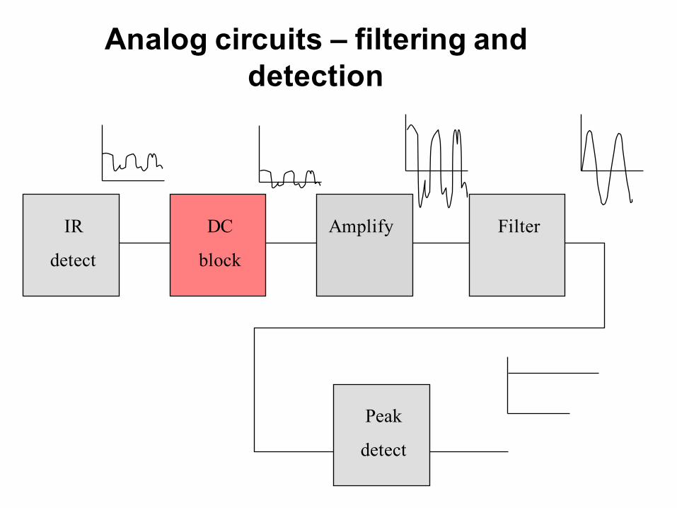
Analog circuits – filtering and detection
IR
detect
DC
block
Amplify Filter
Peak
detect

Analog circuits – DC block
Capacitors:
• Block DC• Pass high frequencies > 1/(2πRC)
R
C

DC blockImaging adding a DC block to your photodetector circuit:
• Which circuit would you build? Why?
1)
2)

Analog circuits – filtering and detection
IR
detect
DC
block
Amplify Filter
Peak
detect

Analog circuits – filtering and detection
What is the result of the following:
+
-Z1
Z2
Z2/Z1= 3
Vout
Vout = 1)
2)
3)
4)
0Vt
V

Analog circuits: Op-ampsEg: Inverting amplifier. +
-V-Vout V- = 0
I1 = Vin/Z1
Vout = 0 – Z2I1
Vout= - (Z2/Z1) Vin
Z1
Z2
Vin
I1
Eg 1: Z2 = 100kΩ
Z1 = 10kΩ Vout= - 10 Vin
Eg 2: Z2 = 100kΩ
Z1 = 1 Ω Vout= - 100,000 Vin !!
Not likely….
10x gain is a “reasonable” value

Analog circuits: Real Op-amps+
-V-Vout
Z1
Z2
Vin
I1
Eg 2: Z2 = 100kΩ
Z1 = 1 Ω Vout= - 100,000 Vin !!
Several problems:
• I1 = 1A for Vin = 1 V !! (excessive load for upstream circuitry)
• Gain Bandwidth product ~ 3 MHz. This would limit the bandwidth of the amplifier from DC up to 30 Hz (i.e. not a very responsive system!).

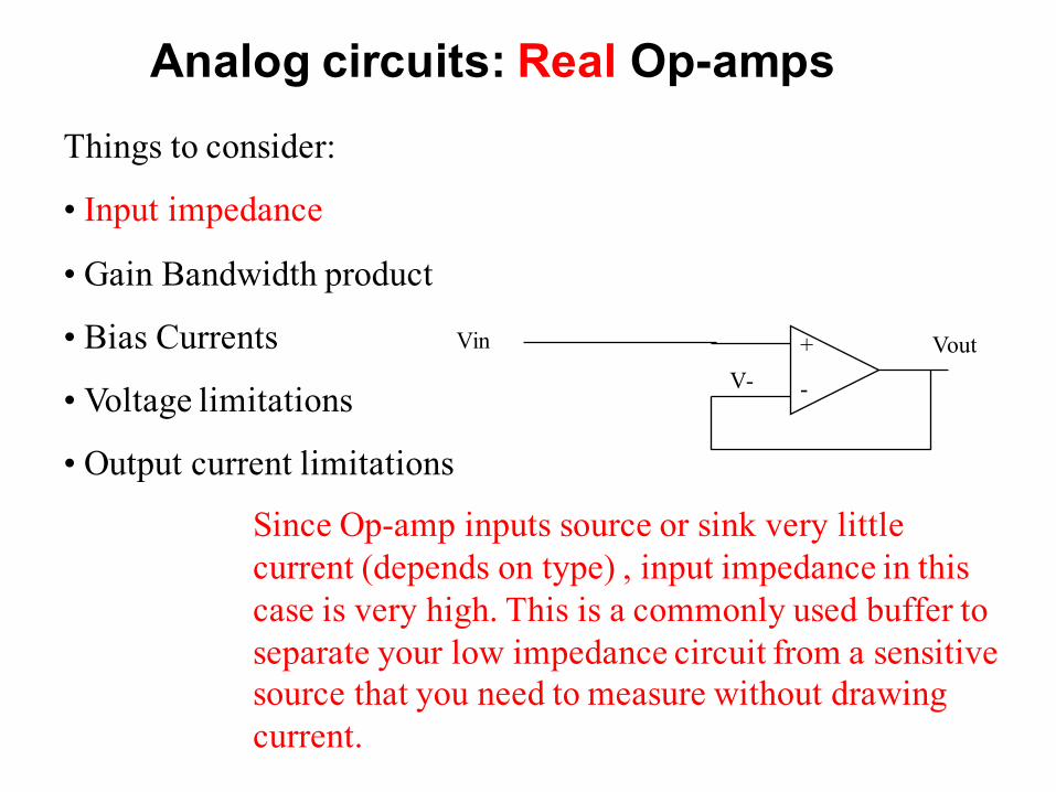
Analog circuits: Real Op-ampsThings to consider:
• Input impedance
• Gain Bandwidth product
• Bias Currents
• Voltage limitations
• Output current limitations
+
-V-Vout
Z1
Z2
Vin
I1
Since V- is a virtual ground, input impedance seen by Vin is Z1
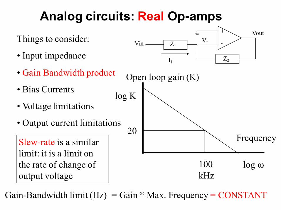
Things to consider:
• Input impedance
• Gain Bandwidth product
• Bias Currents
• Voltage limitations
• Output current limitations
Analog circuits: Real Op-amps
+
-V-VoutVin
Since Op-amp inputs source or sink very little current (depends on type) , input impedance in this case is very high. This is a commonly used buffer to separate your low impedance circuit from a sensitive source that you need to measure without drawing current.

Things to consider:
• Input impedance
• Gain Bandwidth product
• Bias Currents
• Voltage limitations
• Output current limitations
Analog circuits: Real Op-amps+
-V-Vout
Z1
Z2
Vin
I1
Open loop gain (K)
Frequency 20
100 kHz
Gain-Bandwidth limit (Hz) = Gain * Max. Frequency = CONSTANT
Slew-rate is a similar limit: it is a limit on the rate of change of output voltage
log K
log ω

TL082: Gain*Bandwidth = 3 MHzè This means that at a gain of 100, Bandwidth is 30 kHz.
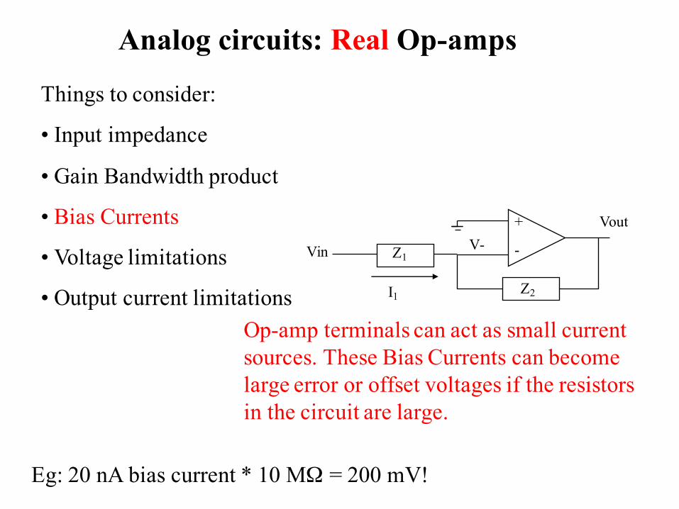
Analog circuits: Real Op-amps
Things to consider:
• Input impedance
• Gain Bandwidth product
• Bias Currents
• Voltage limitations
• Output current limitations
+
-V-Vout
Z1
Z2
Vin
I1
Op-amp terminals can act as small current sources. These Bias Currents can become large error or offset voltages if the resistors in the circuit are large.
Eg: 20 nA bias current * 10 MΩ = 200 mV!

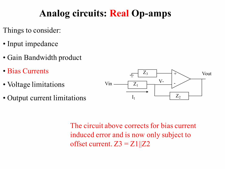
Analog circuits: Real Op-ampsThings to consider:
• Input impedance
• Gain Bandwidth product
• Bias Currents
• Voltage limitations
• Output current limitations
+
-V-Vout
Z1
Z2
Vin
I1
The circuit above corrects for bias current induced error and is now only subject to offset current. Z3 = Z1||Z2
Z3
Analog circuits: Real Op-amps
Things to consider:
• Input impedance
• Gain Bandwidth product
• Bias Currents
• Voltage limitations
• Output current limitations
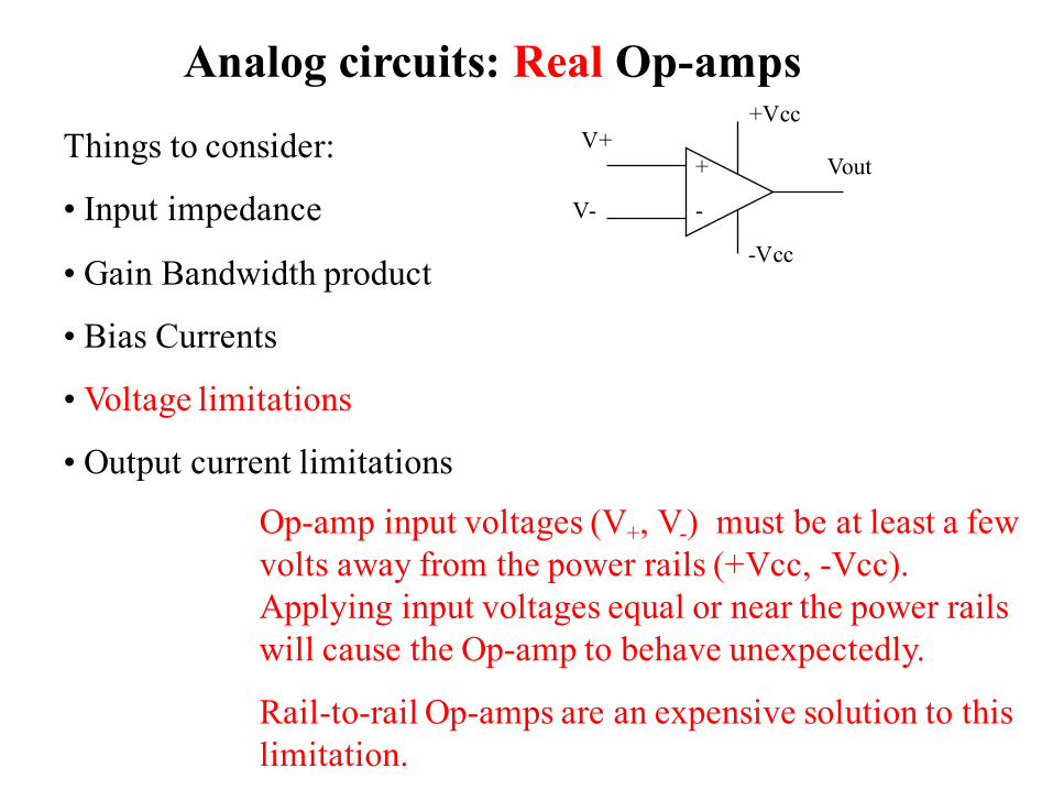
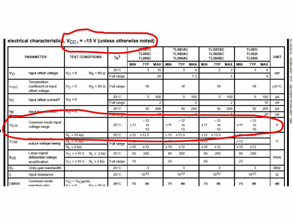
Op-amp input voltages (V+, V-) must be at least a few volts away from the power rails (+Vcc, -Vcc). Applying input voltages equal or near the power rails will cause the Op-amp to behave unexpectedly.
Rail-to-rail Op-amps are an expensive solution to this limitation.
+
-
-Vcc
VoutV+
V-
+Vcc
Analog circuits: Real Op-amps
Things to consider:
• Input impedance
• Gain Bandwidth product
• Bias Currents
• Voltage limitations
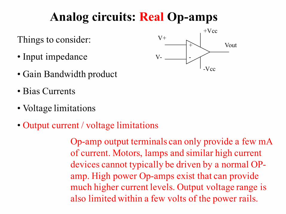
• Output current / voltage limitations
Op-amp output terminals can only provide a few mA of current. Motors, lamps and similar high current devices cannot typically be driven by a normal OP-amp. High power Op-amps exist that can provide much higher current levels. Output voltage range is also limited within a few volts of the power rails.
+
-
-Vcc
VoutV+
V-
+Vcc


Analog circuits: Real Op-amps
Summary:
• Keep resistors in 1K to 500K range unless you really know
what you’re doing.
• Don’t ask a single amplifier to provide huge gains (>30?)
• Don’t drive motors, lamps, or other heavy loads with a
normal op-amp (power op-amps exist for this, or use a
transistor)
• Keep input voltages away from the op-amp voltage rails
(unless using rail-to-rail opamps)

Analog circuits – filtering and detection
IR
detect
DC
block
Amplify Filter
Peak
detect
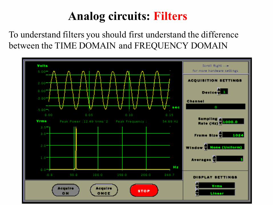
Analog circuits: FiltersTo understand filters you should first understand the difference between the TIME DOMAIN and FREQUENCY DOMAIN

Which is the correct match between the following time-domain (left) signals and their Fourier Transforms (right) ?
a)
b)
c)
d)
i)
ii)
iii)
iv)
1) a-i, b-iv, c-ii, d-iii
2) a-ii, b-iv, c-iii, d-i
3) a-iii, b-iv, c-i, d-ii
4) a-iv, b-ii, c-iii, d-i
t f

Frequency Generator
Spectrum Analyzer
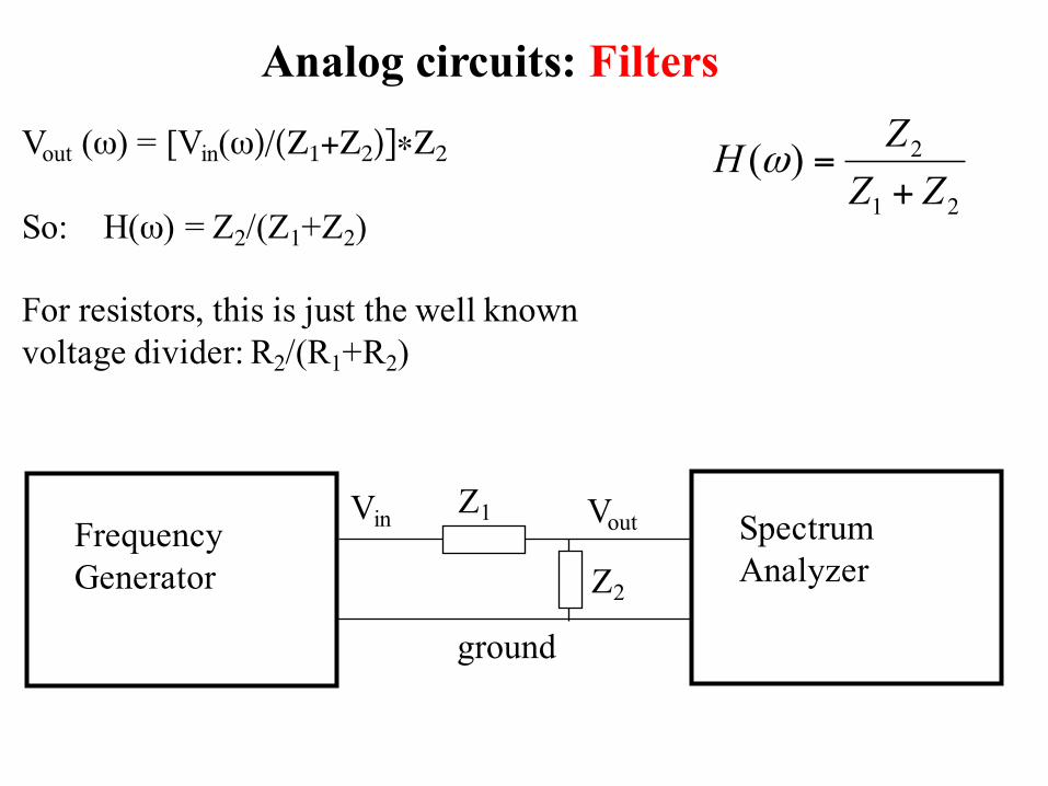
ground
Z1
Z2
Analog circuits: Filters
Vin Vout
“Transfer Function” = Vout/Vin = H(ω)
So: Vout (ω) = H(ω)*Vin(ω)
This is all in terms of ω since, in general, impedances are functions of ω.
Similar to voltage divider: except ω dependent.
Zcap = 1/j ωC
Zind = j ωL
Zres = R
Frequency Generator
Spectrum Analyzer
ground
Z1
Z2
Analog circuits: Filters
Vin Vout
Vout (ω) = [Vin(ω)/(Ζ1+Ζ2)]∗Ζ2
So: H(ω) = Z2/(Z1+Z2)
For resistors, this is just the well known voltage divider: R2/(R1+R2)
21
2)(ZZ
ZH+
=ω

Frequency Generator
Spectrum Analyzer
Z1
Z2
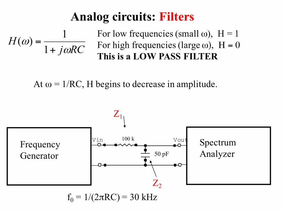
Analog circuits: FiltersNow plug in a resistor and a capacitor:
VoutVinR1
33 k
C1100 nF
100 k
50 nF
Z2 = 1/j ωC
Z1= R
RCj
CjRCjH
ω
ωω
ω
+=
+=
11
/1/1)(
Frequency Generator
Spectrum Analyzer
Z1
Z2
Analog circuits: FiltersFor low frequencies (small ω), H = 1 For high frequencies (large ω), Η = 0This is a LOW PASS FILTER
RCjH
ωω
+=1
1)(
VoutVinR1
33 k
C1100 nF
f0 = 1/(2πRC) = 30 kHz
100 k
50 pF
At ω = 1/RC, H begins to decrease in amplitude.
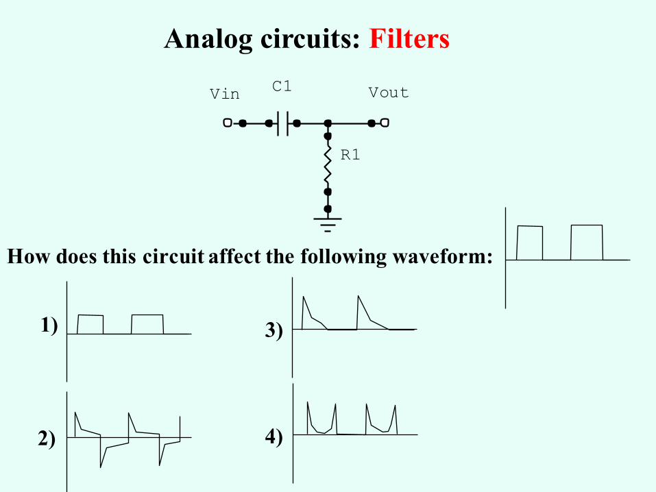
Analog circuits: Filters
VoutVin
R1
C1
How does this circuit affect the following waveform:
1)
2)
3)
4)

Analog circuits: Transfer FunctionsBode plots: a graphical representation of frequency response on logarithmic axes.
20log10(H)
(20 is used instead of 10 so the result will represent power ~ V2)
-3 dB = ½ as much power as 0 dB
Vout is 1/√2 of Vin at -3dB
Vertical axis:
log10(f)Log of frequency is used to ensure linear plots from 1/f or 1/fn functions
Horizontal axis:
Pole: 1/(1+jω/ω0)
Zero: (1+jω/ω0)
-20 db/decade in amplitude after ω0, -90 phase
+20 db/decade in amplitude after ω0, +90 phase

Analog circuits: Simple Pole
RCjH
ωω
+=1
1)(
-3dB, 1/RC - 45 deg, 1/RC
Bode Plot:
-20db/decade
-90 deg
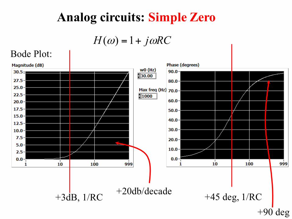
Analog circuits: Simple Zero
RCjH ωω +=1)(
+3dB, 1/RC +45 deg, 1/RC
Bode Plot:
+20db/decade
+90 deg
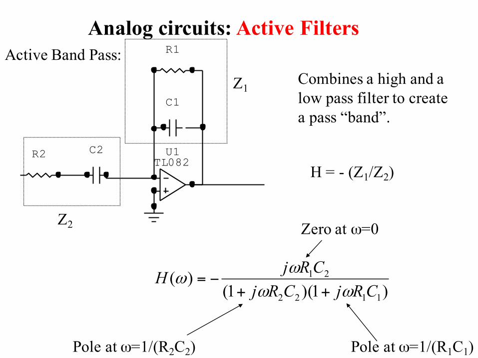
Analog circuits: Active Filters
C2R2
R1
C1
U1TL082
Z2
Z1
)1)(1()(
1122
21
CRjCRjCRjH
ωωω
ω++
−=
Active Band Pass:
Zero at ω=0
Pole at ω=1/(R2C2) Pole at ω=1/(R1C1)
Combines a high and a low pass filter to create a pass “band”.
H = - (Z1/Z2)

Analog circuits: Transfer FunctionsBode plots: a graphical representation of frequency response on logarithmic axes.
Pole: 1/(1+jω/ω0)
Zero: (1+jω/ω0)
-20 db/decade in amplitude after ω0, -90 phase
+20 db/decade in amplitude after ω0, +90 phase
)1)(1()(
1122
21
CRjCRjCRjH
ωωω
ω++
−=
Zero at ω=0
Pole at ω=1/(R2C2) Pole at ω=1/(R1C1)

Analog circuits: Active Filters
)1)(1()(
1122
21
CRjCRjCRjH
ωωω
ω++
−=
Idealized Bode Plot:
Zero at ω=0
Pole at ω=1/(R2C2) Pole at ω=1/(R1C1)
ω
20log(|H|)
0 dB
20log(R1/R2) dB
1/(R2C2) 1/(R1C1)(1)
(2) (3)
(1)
(1)
(1)
(2)
(2) (3) 20db/decade
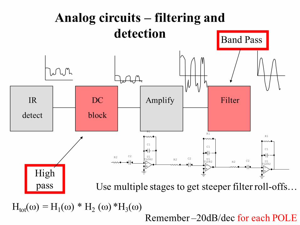
Analog circuits – filtering and detection
IR
detect
DC
block
Amplify Filter
High pass
Band Pass
C2R2
R1
C1
U1TL082 C2R2
R1
C1
U1TL082 C2R2
R1
C1
U1TL082
Use multiple stages to get steeper filter roll-offs…
Htot(ω) = H1(ω) * H2 (ω) *H3(ω) Remember –20dB/dec for each POLE
45
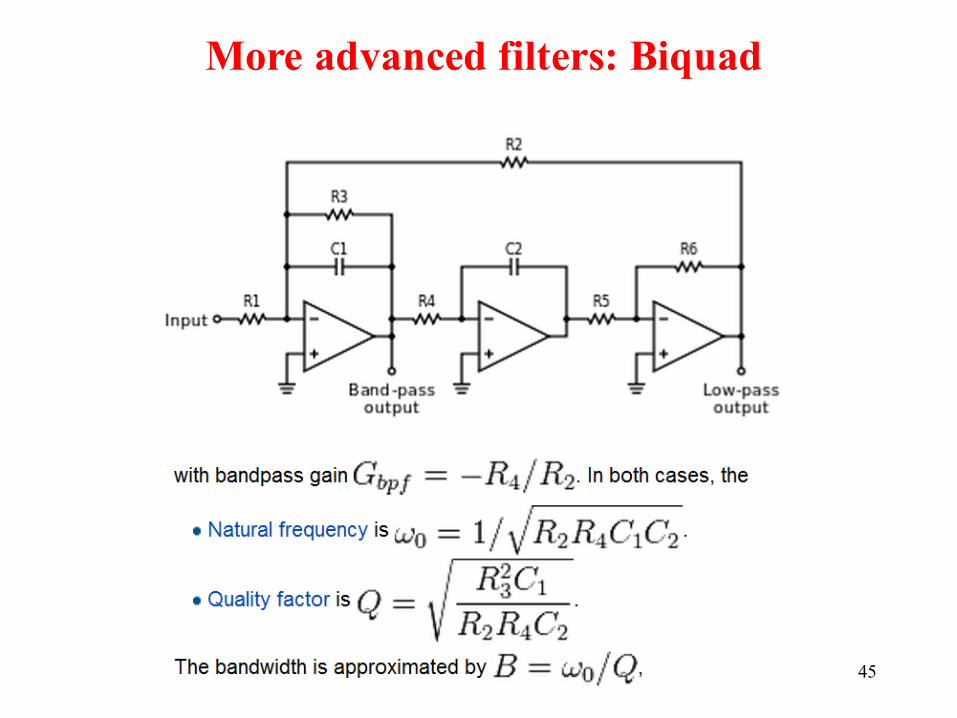
More advanced filters: Biquad
46
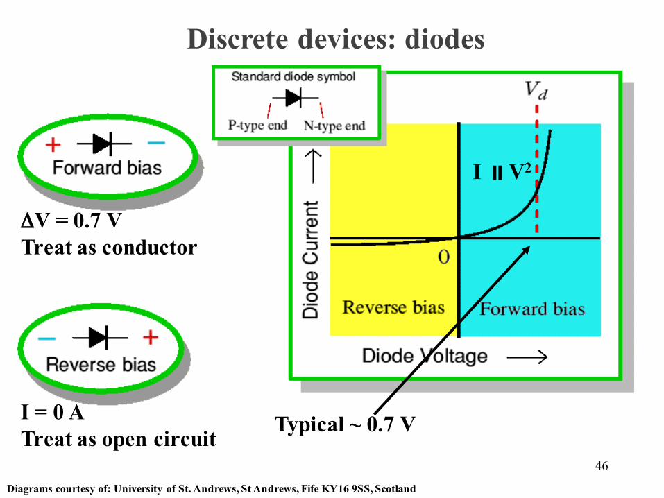
Discrete devices: diodes
Diagrams courtesy of: University of St. Andrews, St Andrews, Fife KY16 9SS, Scotland
Typical ~ 0.7 V
ΔV = 0.7 VTreat as conductor
I = 0 ATreat as open circuit
I ;V2

47
VoutVin
R11k
D1DIODEVin = 5V DC, Vout is connected to
scope only.
a) Vout = 5 V if R1 = 1Kb) Vout = 4.3 V regardless of R1c) Vout = 4.3 V if R1 = 1Kd) Vout = 5 V if R1 is disconnected (infinite resistance)e) Vout = 4.3 V if R1 is disconnected (infinite resistance)
The following are true: (Try it with your own meter)1. a
2. b,c,e
3. c,d
4. a,e
5. c

SUPER-DIODE rectifier circuitThis circuit acts like a perfect diode, without the 0.7V deadbandprior to turn-on.
What bad thing happens if R1 is too big?

Zener Diodes
Use 5V Zener Diodes to protect your TINAH Board
Zener diodes conduct under reverse bias when a specific voltage is exceeded – in our case 5.1V
Zener diodes (5V1)
To TINAH

Debugging CircuitsLearn to systematically check your circuits:• Power rails:
– Check that 15V is really 15V; if not, localize the component that is shorting the power rail. Check power at each chip.
• Physical check: – Check pinouts, missing/loose wires, etc.
• Isolate stages where possible– Check output of stage 1 – if ok plug into stage 2 and see if
stage 1 output is degraded.– If ok, check output of stage 2 etc
• Keep wiring TIDY!
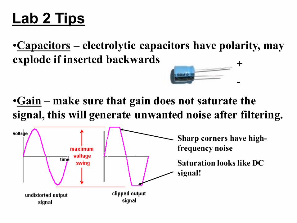
Lab 2 Tips
Sharp corners have high-frequency noise
Saturation looks like DC signal!
+
-
•Capacitors – electrolytic capacitors have polarity, may explode if inserted backwards
•Gain – make sure that gain does not saturate the signal, this will generate unwanted noise after filtering.


