27
Lecture 26: LM3S9B96 Microcontroller – Universal Asynchronous Receivers/Transmitters
| Date post: | 27-Dec-2015 |
| Category: |
Documents |
| Upload: | trevor-milton-hunter |
| View: | 228 times |
| Download: | 2 times |

Lecture 26: LM3S9B96 Microcontroller – Universal Asynchronous Receivers/Transmitters

Stellaris® LM3S9B96 MicrocontrollerData Sheet
Chapter 14Universal Asynchronous Receivers/Transmitters (UARTs)

Universal Asynchronous Receivers/Transmitters (UARTs)
The Stellaris LM3S9B96 controller includes three UARTs with the following features: Programmable baud-rate generator (up to 5Mbps for
regular speed and 10 Mbps for high speed) Separate 16-entry transmit (TX) and receive (RX) FIFOs Programmable FIFO length FIFO trigger levels of 1/8, 1/4, 1/2, 3/4, and 7/8 False-start bit detection Line-break generation and detection Fully programmable serial interface characteristics (data
bits, parity bit, stop bits)

Universal Asynchronous Receivers/Transmitters (UARTs)
IrDA serial-IR (SIR) encoder/decoder providing Support for communication with ISO 7816 smart cards Full modem handshake support (on UART1) LIN protocol support Standard FIFO-level and End-of-Transmission interrupts Efficient transfers using Micro Direct Memory Access
Controller (μDMA)

Block Diagram

Functional Description
Each UART performs the functions of parallel-to-serial and serial-to-parallel conversions
The UART is configured for transmit and/or receive via the TXE and RXE bits of the UART Control (UARTCTL) register, enabled by default
the UART must be disabled by clearing the UARTEN bit in UARTCTL before being programmed
The UART module also includes a serial IR (SIR) encoder/decoder block that can be connected to an infrared transceiver to implement an IrDA SIR physical layer
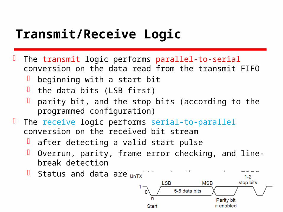
Transmit/Receive Logic
The transmit logic performs parallel-to-serial conversion on the data read from the transmit FIFO beginning with a start bit the data bits (LSB first) parity bit, and the stop bits (according to the programmed
configuration) The receive logic performs serial-to-parallel conversion on the
received bit stream after detecting a valid start pulse Overrun, parity, frame error checking, and line-break
detection Status and data are written to the receive FIFO

Baud-Rate Generation
The baud-rate divisor (BRD) is a 22-bit number a 16-bit integer: can be loaded through the UART Integer
Baud-Rate Divisor (UARTIBRD) register a 6-bit fractional part: can be loaded with the UART
Fractional Baud-Rate Divisor (UARTFBRD) register BRD = BRDI + BRDF = UARTSysClk / (ClkDiv * Baud Rate)
UARTSysClk is the system clock ClkDiv is either 16 (if HSE in UARTCTL is clear) or 8 (if HSE is
set)
BRDI is loaded to UARTIBRD integer(BRDF * 64 + 0.5) is loaded to UARTFBRD

Baud-Rate Generation
The UART generates an internal baud-rate reference clock at 8x (Baud8) or 16x (Baud16) the baud-rate (depending on the setting of the HSE bit (bit 5) in UARTCTL)
This reference clock is divided by 8 or 16 to generate the transmit clock and for error detection during receive operations
any changes to the baud-rate divisor must be followed by a write to a UARTLCRH register for the changes to take effect UARTIBRD write / UARTFBRD write, and UARTLCRH write

Data Transmission
Data received or transmitted is stored in two 16-byte FIFOs
The receive FIFO has an extra four bits per character for status information
For transmitter: data is written into the transmit FIFO If the UART is enabled, a data frame starts
transmitting with the parameters indicated in the UARTLCRH register
The BUSY bit in the UART Flag (UARTFR) register is asserted as soon as there is data in the transmit FIFO
The BUSY bit remains asserted while data is being transmitted until the transmit FIFO is empty
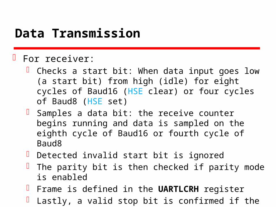
Data Transmission
For receiver: Checks a start bit: When data input goes low (a start
bit) from high (idle) for eight cycles of Baud16 (HSE clear) or four cycles of Baud8 (HSE set)
Samples a data bit: the receive counter begins running and data is sampled on the eighth cycle of Baud16 or fourth cycle of Baud8
Detected invalid start bit is ignored The parity bit is then checked if parity mode is
enabled Frame is defined in the UARTLCRH register Lastly, a valid stop bit is confirmed if the UnRx signal
is High, otherwise a framing error has occurred

FIFO Operation
The UART has two 16-entry FIFOs: one for Rx, one for Tx
Both FIFOs are accessed via the UART Data (UARTDR) register Read operations return a 12-bit value consisting of 8 data
bits and 4 error flags Write operations place 8-bit data in the transmit FIFO Out of reset, both FIFOs are disabled and act as 1-byte-
deep holding registers The FIFOs are enabled by setting the FEN bit in UARTLCRH FIFO status can be monitored via the UART Flag (UARTFR)
register and the UART Receive Status (UARTRSR) register: the UARTFR register contains empty and full flags (TXFE, TXFF, RXFE, and RXFF bits), and the UARTRSR register shows overrun status via the OE bit

FIFO Operation
The trigger points at which the FIFOs generate interrupts is controlled via the UART Interrupt FIFO Level Select (UARTIFLS) register Both FIFOs can be individually configured Available configurations include ⅛, ¼, ½, ¾, and
⅞ For example, if ¾ is selected for the receive FIFO,
the UART generates an interrupt after ¾ X 16 = 12 bytes are received
Out of reset, both FIFOs are configured to trigger an interrupt at the ½ mark
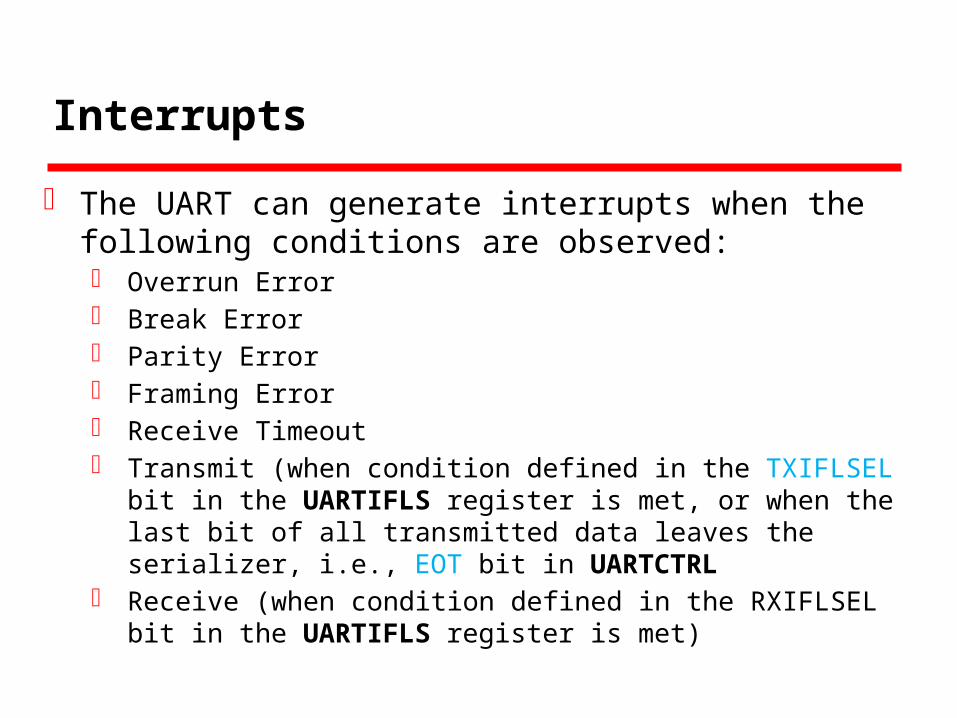
Interrupts
The UART can generate interrupts when the following conditions are observed: Overrun Error Break Error Parity Error Framing Error Receive Timeout Transmit (when condition defined in the TXIFLSEL bit in the
UARTIFLS register is met, or when the last bit of all transmitted data leaves the serializer, i.e., EOT bit in UARTCTRL
Receive (when condition defined in the RXIFLSEL bit in the UARTIFLS register is met)

Interrupts
All of the interrupt events are ORed together before being sent to the interrupt controller
Software can service multiple interrupt events in a single ISR by reading the UART Masked Interrupt Status (UARTMIS) register
The interrupt events can be masked via the UART Interrupt Mask (UARTIM) register
If interrupts are not used, the raw interrupt status is always visible via the UART Raw Interrupt Status (UARTRIS) register

Interrupts
Interrupts are always cleared for both the UARTMIS and UARTRIS registers, when writing a 1 to the corresponding bit in the UART Interrupt Clear (UARTICR) register
When the receive FIFO is not empty, and no further data is received over a 32-bit period, a receive timeout interrupt is asserted
The receive timeout interrupt is cleared: when the FIFO becomes empty through reading
all the data when a 1 is written to the corresponding bit in the
UARTICR register
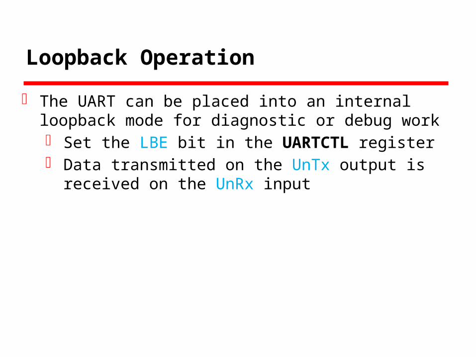
Loopback Operation
The UART can be placed into an internal loopback mode for diagnostic or debug work Set the LBE bit in the UARTCTL register Data transmitted on the UnTx output is received
on the UnRx input

Initialization and Configuration
To enable and initialize the UART, the following steps are necessary: 1. The peripheral clock must be enabled by setting the
UART0, UART1, or UART2 bits in the RCGC1 register 2. The clock to the appropriate GPIO module must be
enabled via the RCGC2 register in the System Control module
3. Set the GPIO AFSEL bits for the appropriate pins 4. Configure the GPIO current level and/or slew rate as
specified for the mode selected 5. Configure the PMCn fields in the GPIOPCTL register to
assign the UART signals to the appropriate pins

Initialization and Configuration
Using UART with an example: the UART clock is 20MHz, 115200 baud rate, data length of 8 bits, one stop bit, no parity, FIFOs disabled, no interrupts
Get the appropriate baud-rate divisor (BRD) first since the UARTIBRD and UARTFBRD registers must be written before the UARTLCRH register
BRD = 20,000,000 / (16 * 115,200) = 10.8507
Therefore, UARTIBRD = 10,
UARTFBRD = integer(0.8507 * 64 + 0.5) = 54

Initialization and Configuration
With the BRD values, the UART configuration is written to the module in the following order: 1. Disable the UART (clear the UARTEN bit in the UARTCTL
register) 2. Write the integer portion of the BRD to the UARTIBRD
register 3. Write the fractional portion of the BRD to the UARTFBRD
register 4. Write the desired serial parameters to the UARTLCRH
register (0x0000 0060 in this case) 5. Enable the UART (set the UARTEN bit in the UARTCTL
register)
NOTE 1: the UART module clock must be enabled before the registers can be programmed
NOTE 2: The UART must be disabled before any of the control registers are reprogrammed

Register Map
The UART’s base address: UART0: 0x4000.C000 UART1: 0x4000.D000 UART2: 0x4000.E000
Table 14-4 on page 596 lists the UART registers. For detailed register descriptions, refer to Chapter
14.6

Register Description: UARTDR
This register is the data register (the interface to the FIFOs). A write to this register initiates a transmission from the
UART The received data can be retrieved by reading this register
Overrun Error: New data was received when the FIFO was full
Break Error: the receive data input was held Low for longer than a full-frame transmission time
Framing Error: The received character does not have a valid stop bit

Register Description: UARTFR
This register is the flag register.
TXFE: UART Transmit FIFO Empty
RXFF: UART Receive FIFO Full
TXFF: UART Transmit FIFO Full
RXFE: UART Receive FIFO Empty
BUSY: UART is busy transmitting data (This bit is set as soon as the transmit FIFO becomes non-empty)

Register Description: UARTLCRH
This register is the line control register Set up serial parameters such as data length, parity, and
stop bit selection When updating the baud-rate divisor (UARTIBRD and/or
UARTIFRD), the UARTLCRH register must also be written
WLEN: UART Word Length, 5, 6, 7, 8 bits
FEN: UART Enable FIFOs
STP2: UART Two Stop Bits Select
EPS: UART Even Parity Select
PEN: UART Parity Enable
BRK: UART Send Break

Register Description: UARTCTL
This register is the control register If software requires a configuration change in the module,
the UARTEN bit must be cleared before the configuration changes are written
Sequence for making changes:1. Disable the UART.2. Wait for the end of transmission or reception of the
current character3. Flush the transmit FIFO by clearing bit 4 (FEN) in the
line control register (UARTLCRH)4. Reprogram the control register5. Enable the UART

Register Description: UARTCTL

Register Description: Others
UART Integer Baud-Rate Divisor (UARTIBRD)
UART Fractional Baud-Rate Divisor (UARTFBRD)UART Interrupt FIFO Level Select (UARTIFLS)UART Interrupt Mask (UARTIM)
UART Raw Interrupt Status (UARTRIS)
UART Masked Interrupt Status (UARTMIS)
UART Interrupt Clear (UARTICR)


