36
EE 3610 Digital Systems Suketu Naik 1 Lecture 3: Modeling in VHDL EE 3610: Digital Systems

EE 3610 Digital Systems Suketu Naik
1
Lecture 3:
Modeling in VHDL
EE 3610: Digital Systems

EE 3610 Digital Systems Suketu Naik
2VHDL: Overview
VHDL
VHSIC Hardware Description Language
VHSIC=Very High Speed Integrated Circuit
Programming language for modelling of hardware
Other languages: Verilog, Verilog-AMS (Analog
and Mixed Signal)

EE 3610 Digital Systems Suketu Naik
3VHDL: Overview
Benefits
Public Standard
Technology and Process Independent
Include technology via libraries
Supports a variety of design methodologies
Behavioral modeling
Dataflow or RTL (Register Transfer Language)
Modeling: We won’t use it
Structural or gate level modeling

EE 3610 Digital Systems Suketu Naik
4VHDL: Overview
Model
Mathematical Description of a physical device
Simulation
Analysis (automated) of a model given a set of inputs
Digital Circuit Models
Structural: defines sub-models and how they are
interconnected (FFs, Gates, etc)
Behavioral: defines the behavior of the circuit (no
actual components)
EE 3610 Digital Systems Suketu Naik
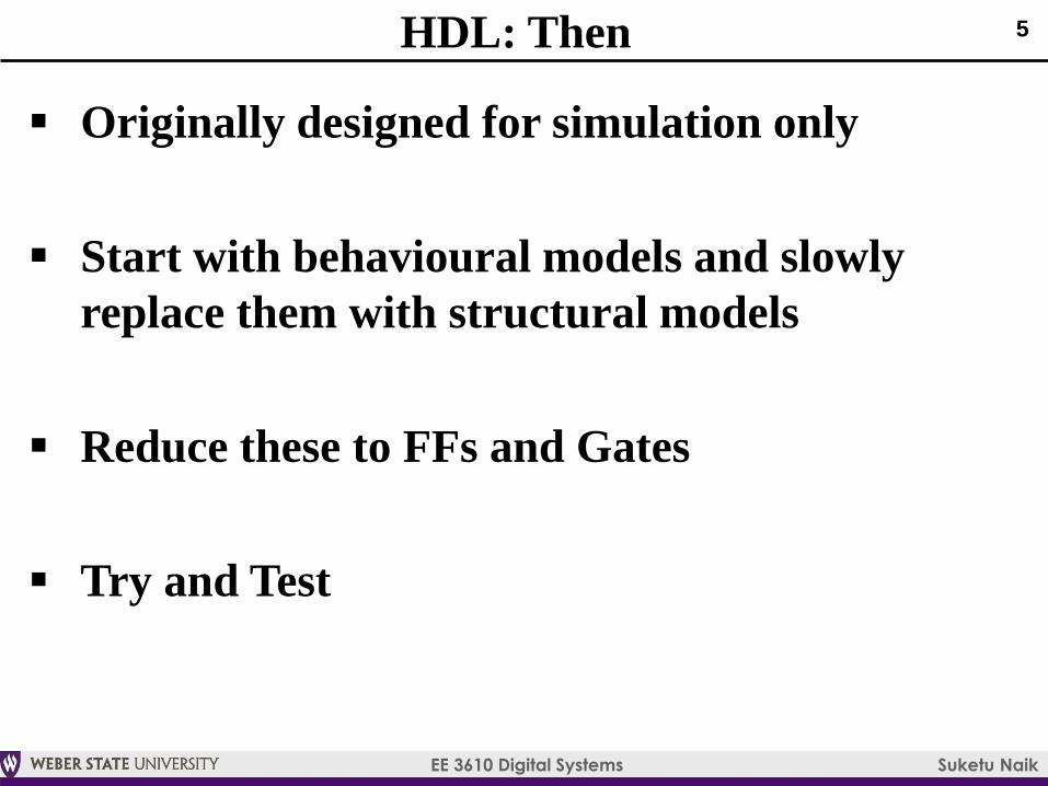
5HDL: Then
Originally designed for simulation only
Start with behavioural models and slowly
replace them with structural models
Reduce these to FFs and Gates
Try and Test

EE 3610 Digital Systems Suketu Naik
6HDL: Now
Build behavioral models and Simulate
Synthesize to net-list (generic)
Fit to a device
Simulate the new (wholly structural) model
Try and test

EE 3610 Digital Systems Suketu Naik
7Levels of Abstraction: Behavioral, Structural, Physical
S <=ABS
Behavioral
(Algorithms, Dataflow)
Structural
(Components,
interconnections)
Physical
EE 3610 Digital Systems Suketu Naik
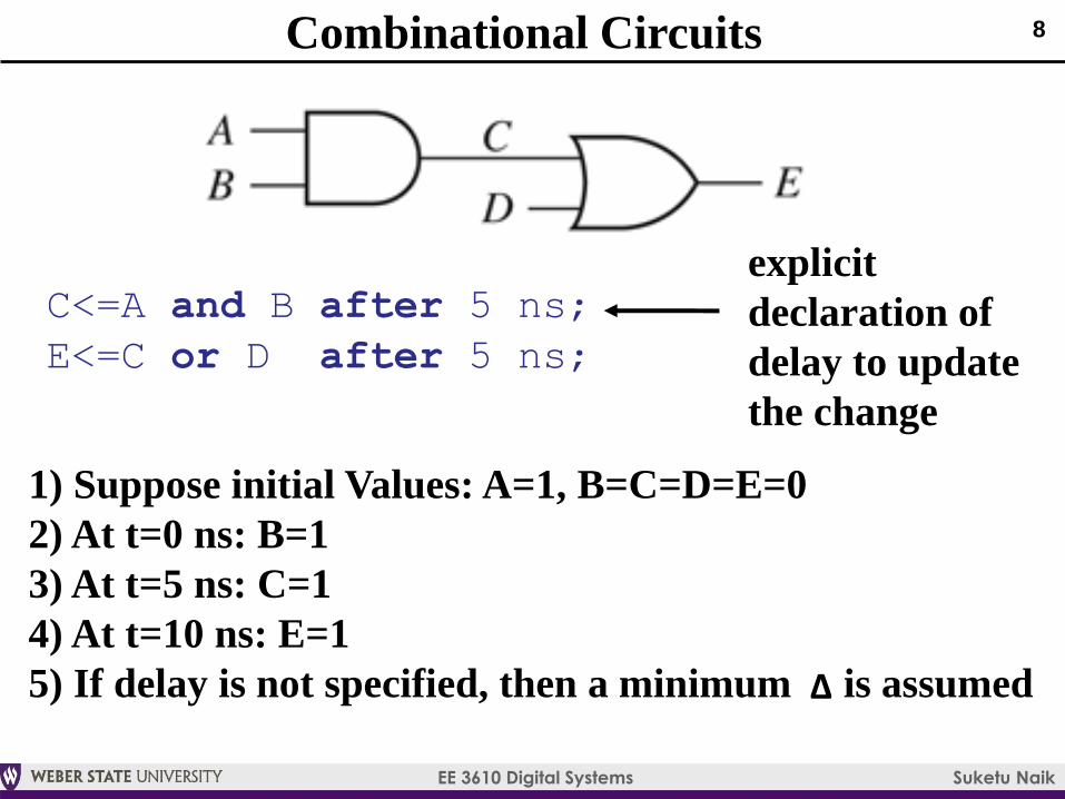
8Combinational Circuits
explicit
declaration of
delay to update
the change
1) Suppose initial Values: A=1, B=C=D=E=0
2) At t=0 ns: B=1
3) At t=5 ns: C=1
4) At t=10 ns: E=1
5) If delay is not specified, then a minimum is assumed∆
C<=A and B after 5 ns;
E<=C or D after 5 ns;

EE 3610 Digital Systems Suketu Naik
9Combinational Circuits
Concurrent Statements
C<=A and B after 5 ns;
E<=C or D after 5 ns;
Order is not important
E<=C or D after 5 ns;
C<=A and B after 5 ns;

EE 3610 Digital Systems Suketu Naik
10Combinational Circuits
This statement causes a simulation error
CLK <= not CLK;

EE 3610 Digital Systems Suketu Naik
11Combinational Circuits
Repetition of Concurrent Statements
1) Implicit Loop
2) Toggles between 1 and 0 after updating the signal at
every 10 ns
3) Will continue indefinitely
CLK <= not CLK after 10 ns;
EE 3610 Digital Systems Suketu Naik
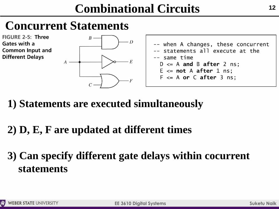
12Combinational Circuits
Concurrent Statements
1) Statements are executed simultaneously
2) D, E, F are updated at different times
3) Can specify different gate delays within cocurrent
statements

EE 3610 Digital Systems Suketu Naik
13VHDL: Elements
Entity:-Description of interface consisting of the port list
-The primary hardware abstraction in VHDL,
-Analogous to a symbol in a block diagram.
Architecture: Description of the function of the
corresponding module.
Process: Allows for a sequential execution of the
assignments
Configuration: Used for simulation purposes.
Package: Hold the definition of commonly used data
types, constants and subprograms.
Library: -The logical name of a collection of compiled
VHDL units (object code)
-Mapped by the simulation or synthesis tools

EE 3610 Digital Systems Suketu Naik
14VHDL: Example Code
Write the code for the following circuit:

EE 3610 Digital Systems Suketu Naik
15VHDL: Example Code
entity example is
port (x1,x2,x3: in std_logic;
f: out std_logic);
end example;
ARCHITECTURE logicFunc of example is
begin -- Architecture statement region
f <= (x1 AND x2) NOR (NOT x2 AND x3);
end logicFunc;
name defined by the user

EE 3610 Digital Systems Suketu Naik
16Code Flow

EE 3610 Digital Systems Suketu Naik
17Code FlowSix Phases
(1) Compilation:
Checks the code to see that the syntax and semantic
rules are met, references to libraries are correct
Outputs intermediate code to be used by Simulator
(2) Elaboration:
A driver is created for each signal
Each driver holds the current value of signal and a queue
of future signal values
Ports are created for each component, memory storage is
allocated, interconnection between port signals specified
EE 3610 Digital Systems Suketu Naik
18Code Flow
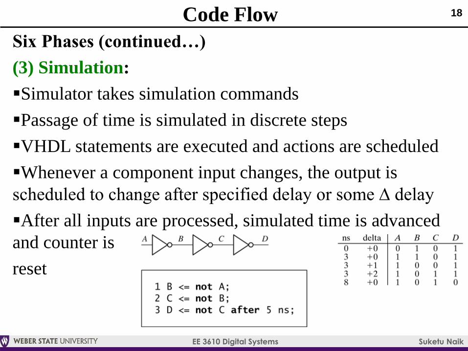
Six Phases (continued…)
(3) Simulation:
Simulator takes simulation commands
Passage of time is simulated in discrete steps
VHDL statements are executed and actions are scheduled
Whenever a component input changes, the output is
scheduled to change after specified delay or some ∆ delay
After all inputs are processed, simulated time is advanced
and counter is
reset

EE 3610 Digital Systems Suketu Naik
19Code Flow
Six Phases (continued…)
(4) Synthesis:
Translate VHDL code to a circuit description
Compilation and Elaboration: same as Simulation
Usually Synthesis comes after Simulation
List of required components and interconnections is
produced
(5) Implementation:
Output of Synthesizer is used to implement the digital
system using specific hardware, e.g. CPLD, FPGA, ASIC
ASIC: masks may be generated
CPLD/FPGA: generates bit-map

EE 3610 Digital Systems Suketu Naik
20Code Flow
(5) Implementation (continued…):
TRANSLATE: converts the netlist generated from the synthesis
process, into a form specific to the target device (e.g. Xilinx
FPGA).
MAP: translates the standard building blocks into the specific
resources available in the target hardware
PLACE & ROUTE: picks up where the MAP process leaves off
by allocating specific resources (placing) and interconnecting
(routing) the placed design, places and routes the design to the
timing constraints
Can perform a post-place and route simulation
(6) Hardware:
Binary programming file is generated (bitstream) and
downloaded to the FPGA

EE 3610 Digital Systems Suketu Naik
21Inside of a Bit File: Lab 0
Hexadecimal Format

EE 3610 Digital Systems Suketu Naik
22SIDE NOTES: INSIDE THE FPGA
EE 3610 Digital Systems Suketu Naik
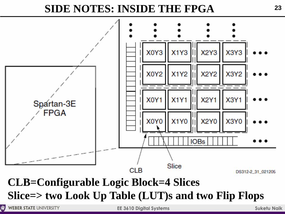
23SIDE NOTES: INSIDE THE FPGA
CLB=Configurable Logic Block=4 Slices
Slice=> two Look Up Table (LUT)s and two Flip Flops
EE 3610 Digital Systems Suketu Naik
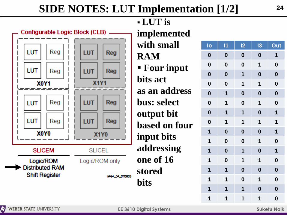
24SIDE NOTES: LUT Implementation [1/2]
LUT is
implemented
with small
RAM
Four input
bits act
as an address
bus: select
output bit
based on four
input bits
addressing
one of 16
stored
bits
Io I1 I2 I3 Out
0 0 0 0 1
0 0 0 1 0
0 0 1 0 0
0 0 1 1 0
0 1 0 0 0
0 1 0 1 0
0 1 1 0 1
0 1 1 1 1
1 0 0 0 1
1 0 0 1 0
1 0 1 0 1
1 0 1 1 0
1 1 0 0 0
1 1 0 1 0
1 1 1 0 0
1 1 1 1 0
EE 3610 Digital Systems Suketu Naik
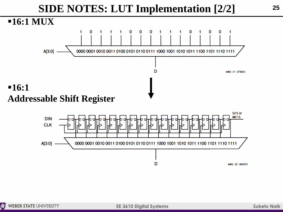
25
16:1 MUX
16:1
Addressable Shift Register
SIDE NOTES: LUT Implementation [2/2]
EE 3610 Digital Systems Suketu Naik
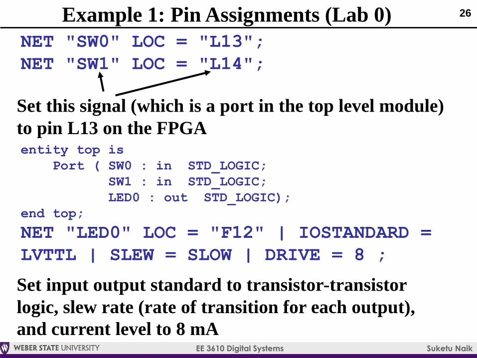
26Example 1: Pin Assignments (Lab 0)
NET "SW0" LOC = "L13";
NET "SW1" LOC = "L14";
entity top is
Port ( SW0 : in STD_LOGIC;
SW1 : in STD_LOGIC;
LED0 : out STD_LOGIC);
end top;
NET "LED0" LOC = "F12" | IOSTANDARD =
LVTTL | SLEW = SLOW | DRIVE = 8 ;
Set this signal (which is a port in the top level module)
to pin L13 on the FPGA
Set input output standard to transistor-transistor
logic, slew rate (rate of transition for each output),
and current level to 8 mA
EE 3610 Digital Systems Suketu Naik
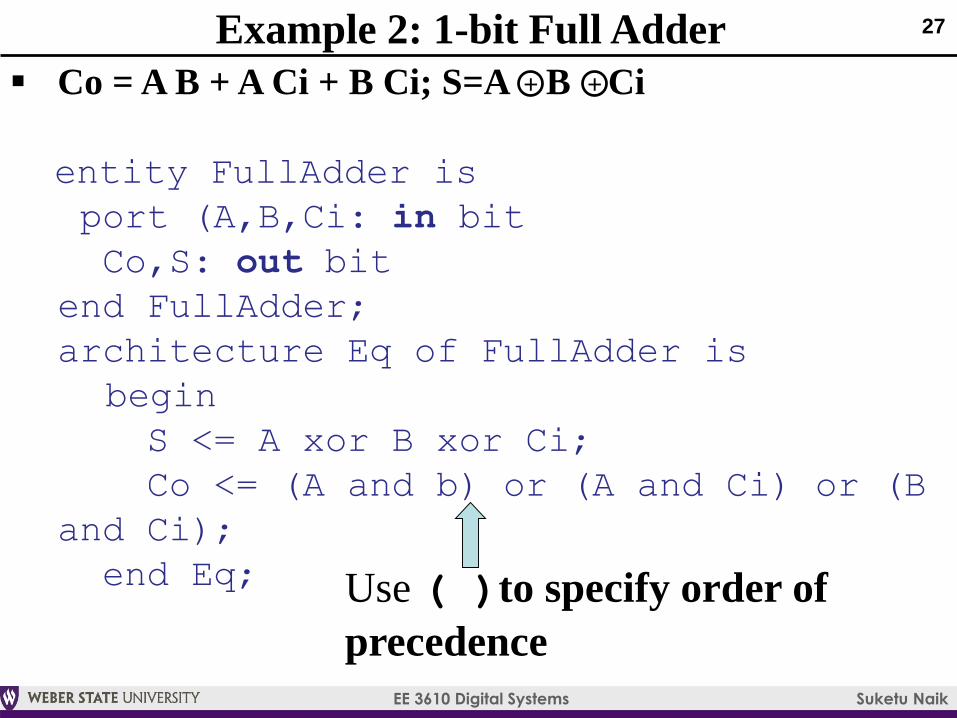
27Example 2: 1-bit Full Adder
Co = A B + A Ci + B Ci; S=A B Ci
entity FullAdder is
port (A,B,Ci: in bit
Co,S: out bit
end FullAdder;
architecture Eq of FullAdder is
begin
S <= A xor B xor Ci;
Co <= (A and b) or (A and Ci) or (B
and Ci);
end Eq;
+ +
Use ( )to specify order of
precedence
EE 3610 Digital Systems Suketu Naik
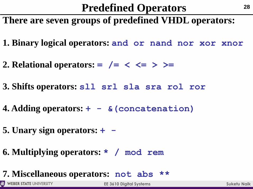
28Predefined OperatorsThere are seven groups of predefined VHDL operators:
1. Binary logical operators: and or nand nor xor xnor
2. Relational operators: = /= < <= > >=
3. Shifts operators: sll srl sla sra rol ror
4. Adding operators: + - &(concatenation)
5. Unary sign operators: + -
6. Multiplying operators: * / mod rem
7. Miscellaneous operators: not abs **

EE 3610 Digital Systems Suketu Naik
29Predefined Operators: Order of Precedence [1/2]Highest precedence first,
left to right within same precedence group,
use parenthesis to control order.
Unary operators take an operand on the right.
"result same" means the result is the same as the right operand.
Binary operators take an operand on the left and right.
"result same" means the result is the same as the left operand.
** exponentiation, numeric ** integer, result numeric
abs absolute value, abs numeric, result numeric
not complement, not logic or boolean, result same
* multiplication, numeric * numeric, result numeric
/ division, numeric / numeric, result numeric
mod modulo, integer mod integer, result integer
rem remainder, integer rem integer, result integer
+ unary plus, + numeric, result numeric
- unary minus, - numeric, result numeric
+ addition, numeric + numeric, result numeric
- subtraction, numeric - numeric, result numeric
& concatenation, array or element & array or element,
result array
Reserved Words: http://www.xilinx.com/itp/xilinx10/isehelp/ite_r_vhdl_reserved_words.htm
EE 3610 Digital Systems Suketu Naik
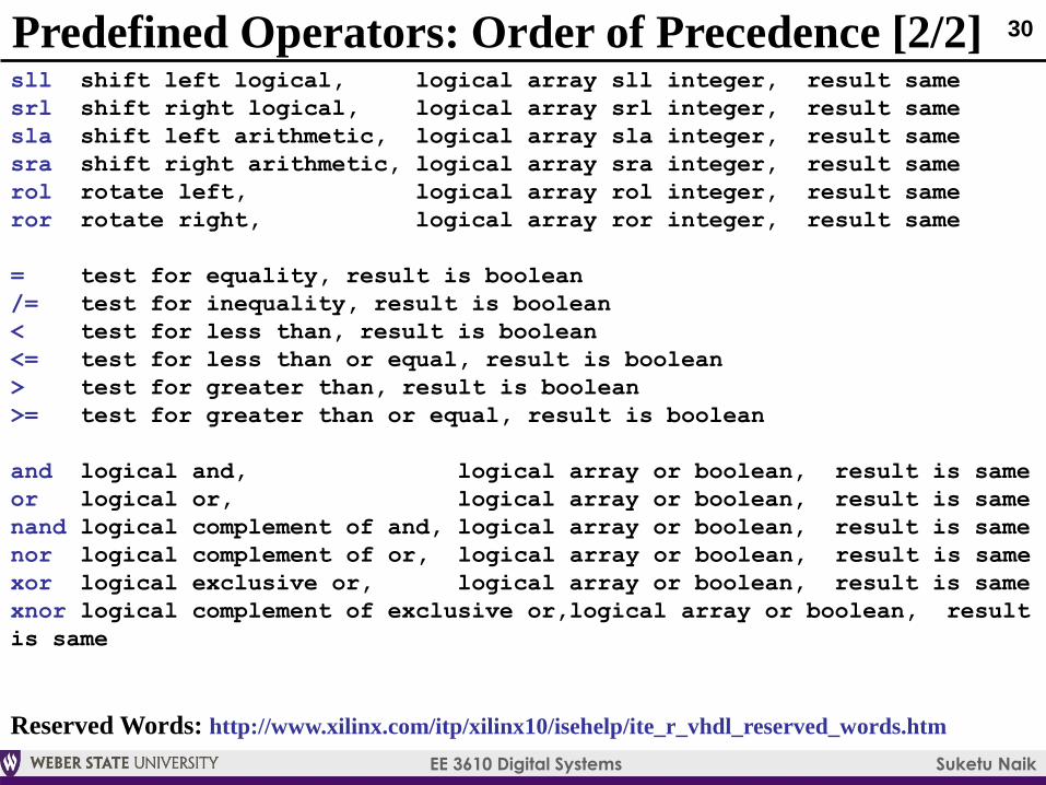
30Predefined Operators: Order of Precedence [2/2]sll shift left logical, logical array sll integer, result same
srl shift right logical, logical array srl integer, result same
sla shift left arithmetic, logical array sla integer, result same
sra shift right arithmetic, logical array sra integer, result same
rol rotate left, logical array rol integer, result same
ror rotate right, logical array ror integer, result same
= test for equality, result is boolean
/= test for inequality, result is boolean
< test for less than, result is boolean
<= test for less than or equal, result is boolean
> test for greater than, result is boolean
>= test for greater than or equal, result is boolean
and logical and, logical array or boolean, result is same
or logical or, logical array or boolean, result is same
nand logical complement of and, logical array or boolean, result is same
nor logical complement of or, logical array or boolean, result is same
xor logical exclusive or, logical array or boolean, result is same
xnor logical complement of exclusive or,logical array or boolean, result
is same
Reserved Words: http://www.xilinx.com/itp/xilinx10/isehelp/ite_r_vhdl_reserved_words.htm

EE 3610 Digital Systems Suketu Naik
31Example 3: Priority of Operators
Let A=”110”, B=”111”, C=”011000”, and D=”111011”
(A & not B or C ror 2 and D)=“110010”
Order: not, &, ror, or, and, = 1) not B = ‘000” --bit-by-bit complement
2) A & not B = “110000” --concatenation
3) C ror 2 = “000110” --rotate right 2
places
4) (A & not B) or (C ror 2) = “110110 --bit-by-bit or
5) (A & not B or C ror 2) and D = “110010”--bit-by-bit and
6) [(A & not B or C ror 2 and D) =
“110010”]=TRUE=1 --with parentheses the equality test is done last

EE 3610 Digital Systems Suketu Naik
32Example 4: Concurrent Statement (4-bit mux)
entity mux4 is
port (I0, I1, I2, I3: in std_logic;
Select: in std_logic_vector (1
downto 0);
Y: out bit);
end mux4;
architecture dude of mux4 is
begin
Y <= I0 when select =‘00’;
else I1 when select =‘01’;
else I2 when select =‘10’;
else I3;
end dude;

EE 3610 Digital Systems Suketu Naik
4 bit Ripple Carry Adder
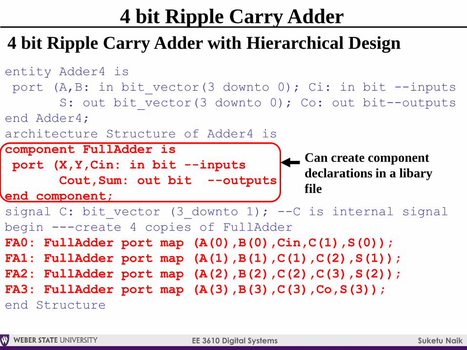
EE 3610 Digital Systems Suketu Naik
4 bit Ripple Carry Adder
entity Adder4 is
port (A,B: in bit_vector(3 downto 0); Ci: in bit --inputs
S: out bit_vector(3 downto 0); Co: out bit--outputs
end Adder4;
architecture Structure of Adder4 is
component FullAdder is
port (X,Y,Cin: in bit --inputs
Cout,Sum: out bit --outputs
end component;
signal C: bit_vector (3_downto 1); --C is internal signal
begin ---create 4 copies of FullAdder
FA0: FullAdder port map (A(0),B(0),Cin,C(1),S(0));
FA1: FullAdder port map (A(1),B(1),C(1),C(2),S(1));
FA2: FullAdder port map (A(2),B(2),C(2),C(3),S(2));
FA3: FullAdder port map (A(3),B(3),C(3),Co,S(3));
end Structure
Can create component
declarations in a libary
file
4 bit Ripple Carry Adder with Hierarchical Design
EE 3610 Digital Systems Suketu Naik
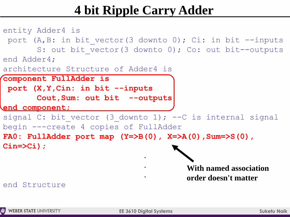
4 bit Ripple Carry Adder
entity Adder4 is
port (A,B: in bit_vector(3 downto 0); Ci: in bit --inputs
S: out bit_vector(3 downto 0); Co: out bit--outputs
end Adder4;
architecture Structure of Adder4 is
component FullAdder is
port (X,Y,Cin: in bit --inputs
Cout,Sum: out bit --outputs
end component;
signal C: bit_vector (3_downto 1); --C is internal signal
begin ---create 4 copies of FullAdder
FA0: FullAdder port map (Y=>B(0), X=>A(0),Sum=>S(0),
Cin=>Ci);
.
.
.
end Structure
With named association
order doesn't matter

EE 3610 Digital Systems Suketu Naik
36VHDL: Common Mistakes
Avoid Common Mistakes:[1] http://class.ece.iastate.edu/cpre583/ref/VHDL/Common_VHDL_mistakes.pdf
[2] https://engineering.purdue.edu/~ece437l/papers/VHDL_Dos_and_Donts.ppt
VHDL Guides:[1] http://www.ics.uci.edu/~jmoorkan/vhdlref/vhdl_golden_reference_guide.pdf


