37
Lecture 3: Nonideal Transistor Theory
| Date post: | 31-Dec-2015 |
| Category: |
Documents |
| Upload: | jonah-blankenship |
| View: | 241 times |
| Download: | 1 times |
Lecture 3: Nonideal Transistor Theory
4: Nonideal Transistor Theory 2CMOS VLSI DesignCMOS VLSI Design 4th Ed.
Outline Nonideal Transistor Behavior
– High Field Effects• Mobility Degradation• Velocity Saturation
– Channel Length Modulation– Threshold Voltage Effects
• Body Effect• Drain-Induced Barrier Lowering• Short Channel Effect
– Leakage• Subthreshold Leakage• Gate Leakage• Junction Leakage
Process and Environmental Variations
4: Nonideal Transistor Theory 3CMOS VLSI DesignCMOS VLSI Design 4th Ed.
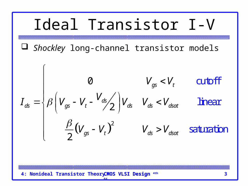
Ideal Transistor I-V Shockley long-channel transistor models
2
cutoff
linear
saturatio
0
2
2n
gs t
dsds gs t ds ds dsat
gs t ds dsat
V V
VI V V V V V
V V V V
4: Nonideal Transistor Theory 4CMOS VLSI DesignCMOS VLSI Design 4th Ed.
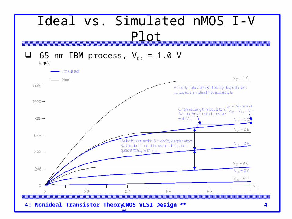
Ideal vs. Simulated nMOS I-V Plot
65 nm IBM process, VDD = 1.0 V
0 0.2 0.4 0.6 0.8 1
0
200
400
600
800
1000
1200
Vds
Ids (A)
Vgs = 1.0
Vgs = 1.0
Vgs = 0.8
Vgs = 0.6
Vgs = 0.4
Vgs = 0.8
Vgs = 0.6
Channel length modulation:Saturation current increases with Vds
Ion = 747 mA @ Vgs = Vds = VDD
Simulated
Ideal
Velocity saturation & Mobility degradation: Saturation current increases less than quadratically with Vgs
Velocity saturation & Mobility degradation: Ion lower than ideal model predicts
4: Nonideal Transistor Theory 5CMOS VLSI DesignCMOS VLSI Design 4th Ed.
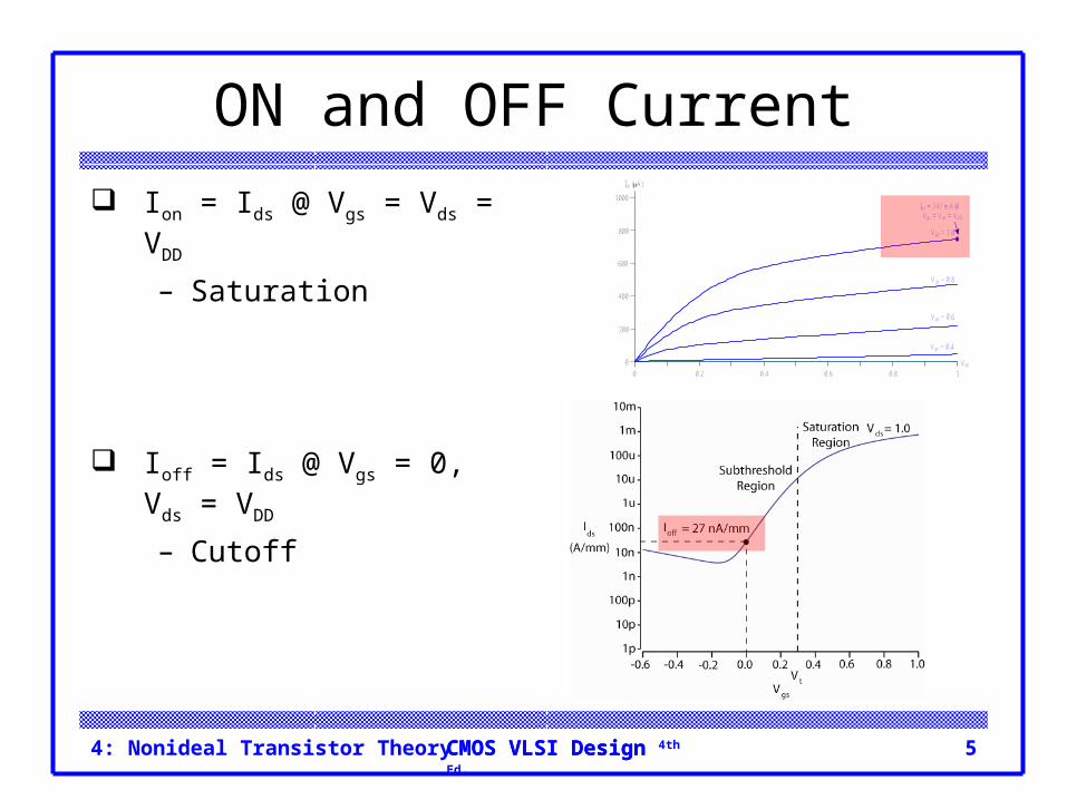
ON and OFF Current Ion = Ids @ Vgs = Vds = VDD
– Saturation
Ioff = Ids @ Vgs = 0, Vds = VDD
– Cutoff
0 0.2 0.4 0.6 0.8 1
0
200
400
600
800
1000
Vds
Ids (A)
Vgs = 1.0
Vgs = 0.4
Vgs = 0.8
Vgs = 0.6
Ion = 747 mA @ Vgs = Vds = VDD
4: Nonideal Transistor Theory 6CMOS VLSI DesignCMOS VLSI Design 4th Ed.
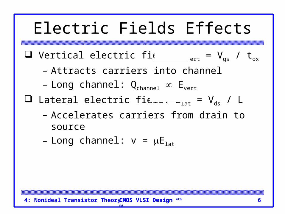
Electric Fields Effects
Vertical electric field: Evert = Vgs / tox
– Attracts carriers into channel
– Long channel: Qchannel Evert
Lateral electric field: Elat = Vds / L
– Accelerates carriers from drain to source
– Long channel: v = Elat
4: Nonideal Transistor Theory 7CMOS VLSI DesignCMOS VLSI Design 4th Ed.
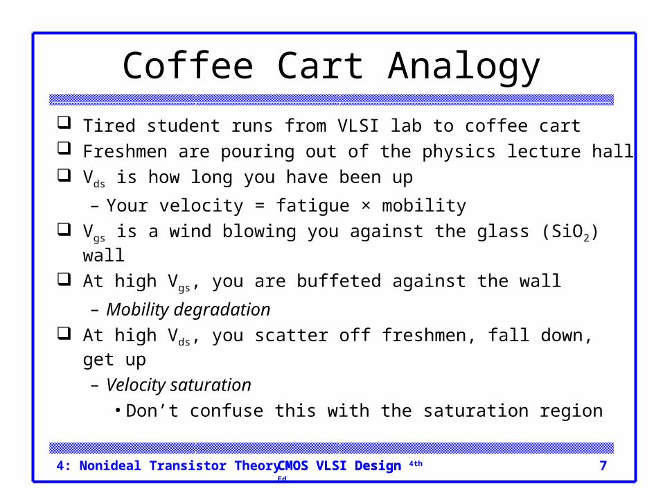
Coffee Cart Analogy
Tired student runs from VLSI lab to coffee cart Freshmen are pouring out of the physics lecture hall Vds is how long you have been up
– Your velocity = fatigue × mobility Vgs is a wind blowing you against the glass (SiO2) wall
At high Vgs, you are buffeted against the wall
– Mobility degradation At high Vds, you scatter off freshmen, fall down, get up
– Velocity saturation• Don’t confuse this with the saturation region
4: Nonideal Transistor Theory 8CMOS VLSI DesignCMOS VLSI Design 4th Ed.
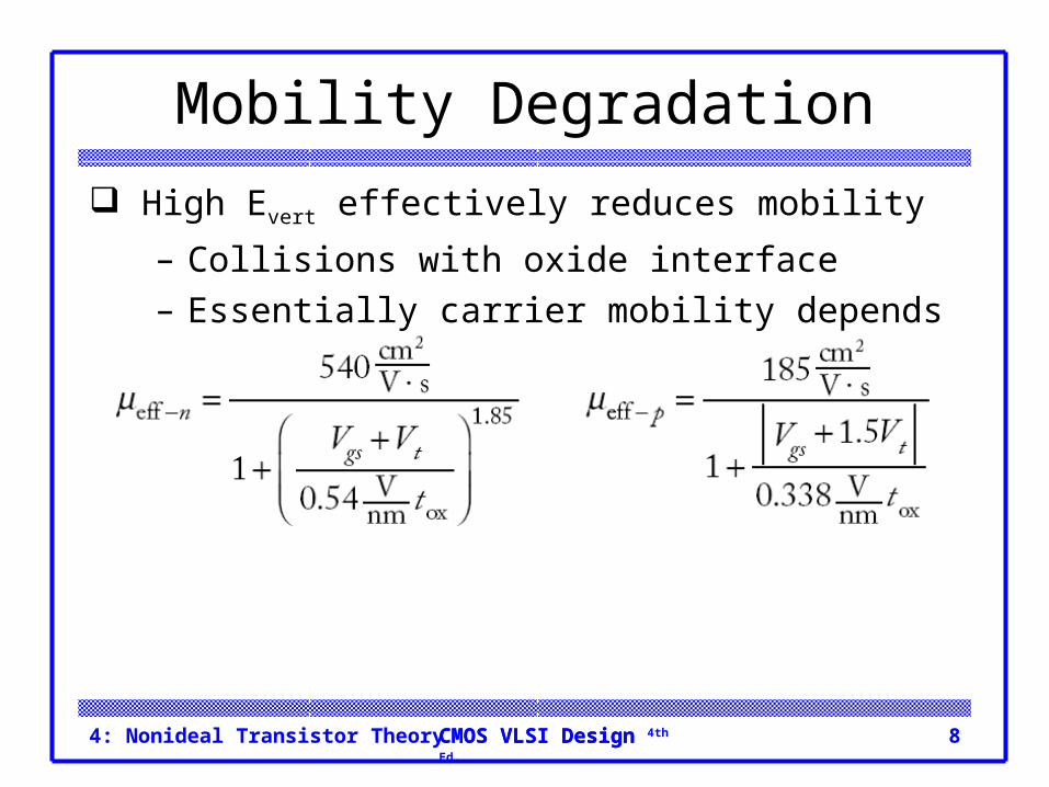
Mobility Degradation
High Evert effectively reduces mobility
– Collisions with oxide interface
– Essentially carrier mobility depends on Vgs and Vt
4: Nonideal Transistor Theory 9CMOS VLSI DesignCMOS VLSI Design 4th Ed.
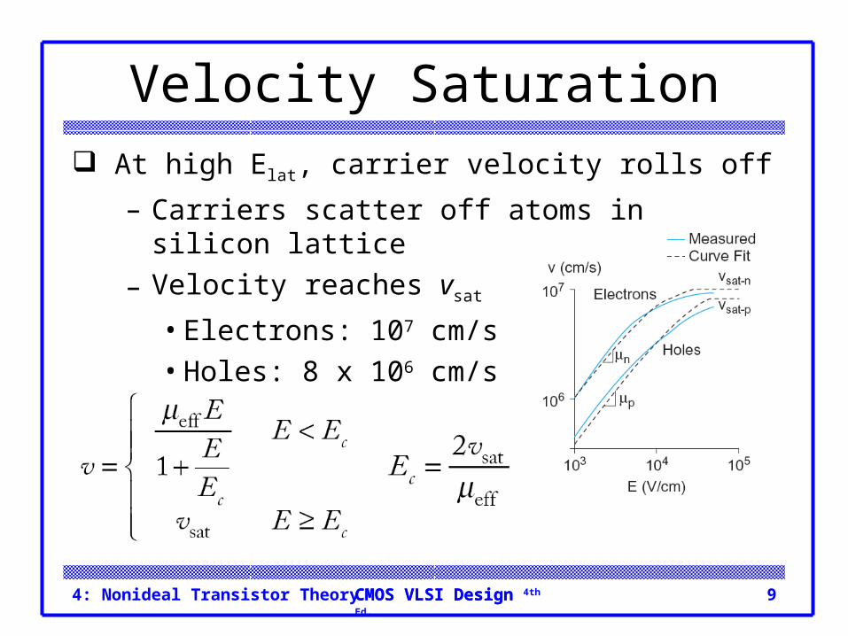
Velocity Saturation At high Elat, carrier velocity rolls off
– Carriers scatter off atoms in silicon lattice
– Velocity reaches vsat
• Electrons: 107 cm/s• Holes: 8 x 106 cm/s
– Better model
4: Nonideal Transistor Theory 10CMOS VLSI DesignCMOS VLSI Design 4th Ed.
Example 1
Calculate the effective carrier mobilities of nMOS and pMOS transistors when fully ON. Assume Vgs = 1 V, Vt = 0.3 V and tox = 1.05 nm
4: Nonideal Transistor Theory 11CMOS VLSI DesignCMOS VLSI Design 4th Ed.
Example 2
Find the critical voltage for nMOS and pMOS transistors that are fully ON, using the values obtained in example 1 and L = 50nm.
(Hint Vc = Ec●L) Which transistor is more vulnerable to velocity
saturation?
4: Nonideal Transistor Theory 12CMOS VLSI DesignCMOS VLSI Design 4th Ed.
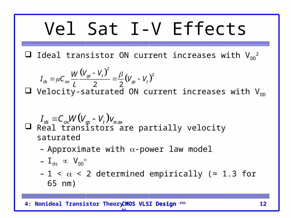
Vel Sat I-V Effects Ideal transistor ON current increases with VDD
2
Velocity-saturated ON current increases with VDD
Real transistors are partially velocity saturated– Approximate with -power law model
– Ids VDD
– 1 < < 2 determined empirically (≈ 1.3 for 65 nm)
2
2
ox 2 2gs t
ds gs t
V VWI C V V
L
ox maxds gs tI C W V V v
4: Nonideal Transistor Theory 13CMOS VLSI DesignCMOS VLSI Design 4th Ed.
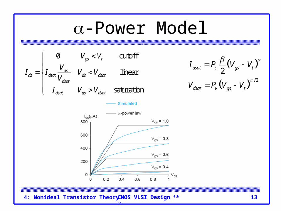
-Power Model0 cutoff
linear
saturation
gs t
dsds dsat ds dsat
dsat
dsat ds dsat
V V
VI I V V
V
I V V
/ 2
2dsat c gs t
dsat v gs t
I P V V
V P V V
4: Nonideal Transistor Theory 14CMOS VLSI DesignCMOS VLSI Design 4th Ed.
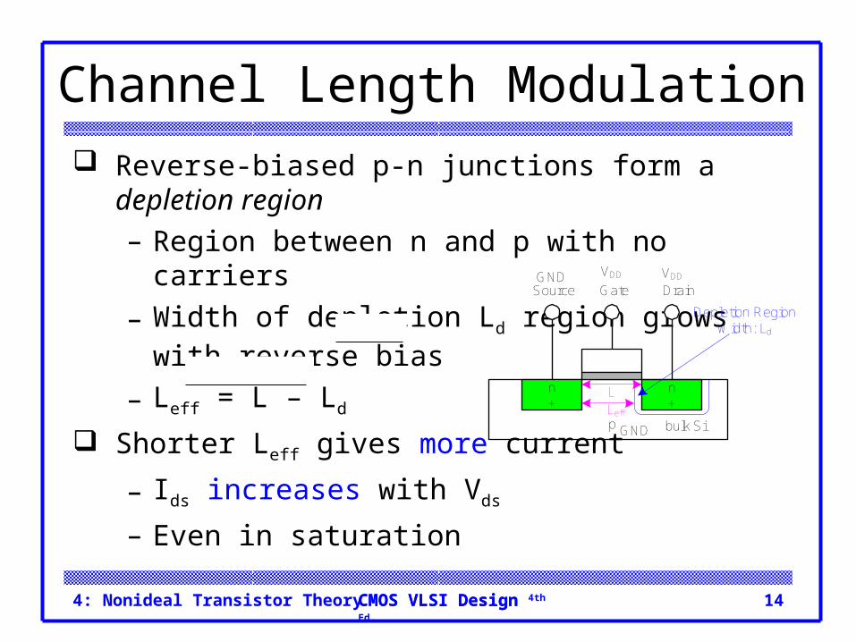
Channel Length Modulation Reverse-biased p-n junctions form a depletion region
– Region between n and p with no carriers
– Width of depletion Ld region grows with reverse bias
– Leff = L – Ld
Shorter Leff gives more current
– Ids increases with Vds
– Even in saturation
n+
p
GateSource Drain
bulk Si
n+
VDDGND VDD
GND
LLeff
Depletion RegionWidth: Ld
4: Nonideal Transistor Theory 15CMOS VLSI DesignCMOS VLSI Design 4th Ed.
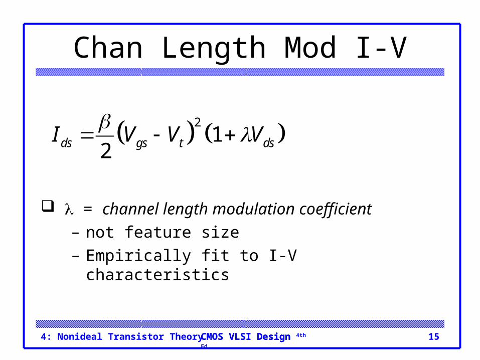
Chan Length Mod I-V
= channel length modulation coefficient– not feature size– Empirically fit to I-V characteristics
21
2ds gs t dsI V V V
4: Nonideal Transistor Theory 16CMOS VLSI DesignCMOS VLSI Design 4th Ed.
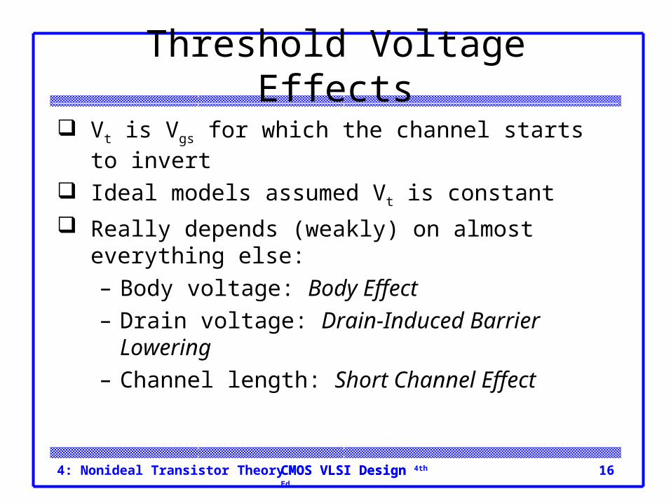
Threshold Voltage Effects
Vt is Vgs for which the channel starts to invert
Ideal models assumed Vt is constant
Really depends (weakly) on almost everything else:– Body voltage: Body Effect– Drain voltage: Drain-Induced Barrier Lowering– Channel length: Short Channel Effect
4: Nonideal Transistor Theory 17CMOS VLSI DesignCMOS VLSI Design 4th Ed.
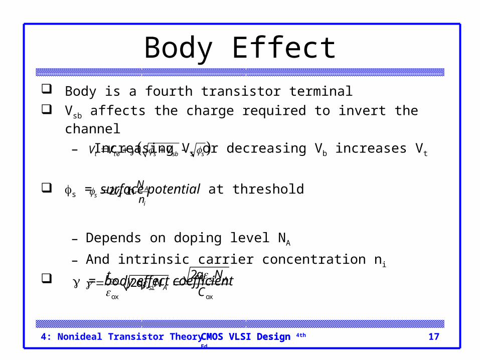
Body Effect Body is a fourth transistor terminal Vsb affects the charge required to invert the channel
– Increasing Vs or decreasing Vb increases Vt
s = surface potential at threshold
– Depends on doping level NA
– And intrinsic carrier concentration ni
= body effect coefficient
0t t s sb sV V V
2 ln As T
i
Nv
n
sioxsi
ox ox
2q2q A
A
NtN
C
4: Nonideal Transistor Theory 18CMOS VLSI DesignCMOS VLSI Design 4th Ed.
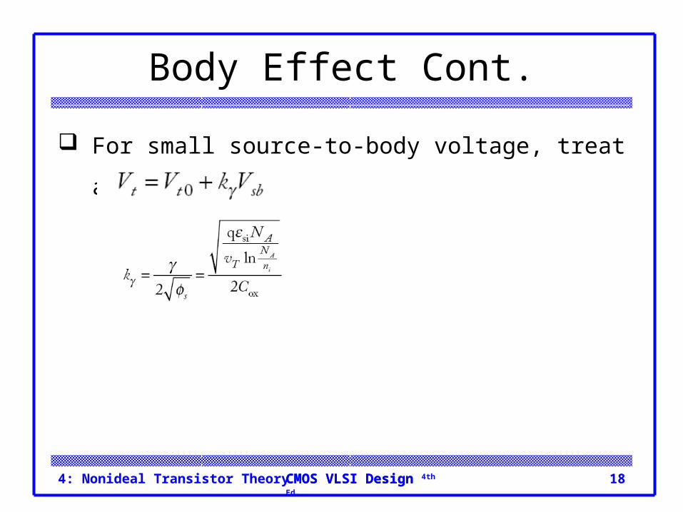
Body Effect Cont.
For small source-to-body voltage, treat as linear
4: Nonideal Transistor Theory 19CMOS VLSI DesignCMOS VLSI Design 4th Ed.
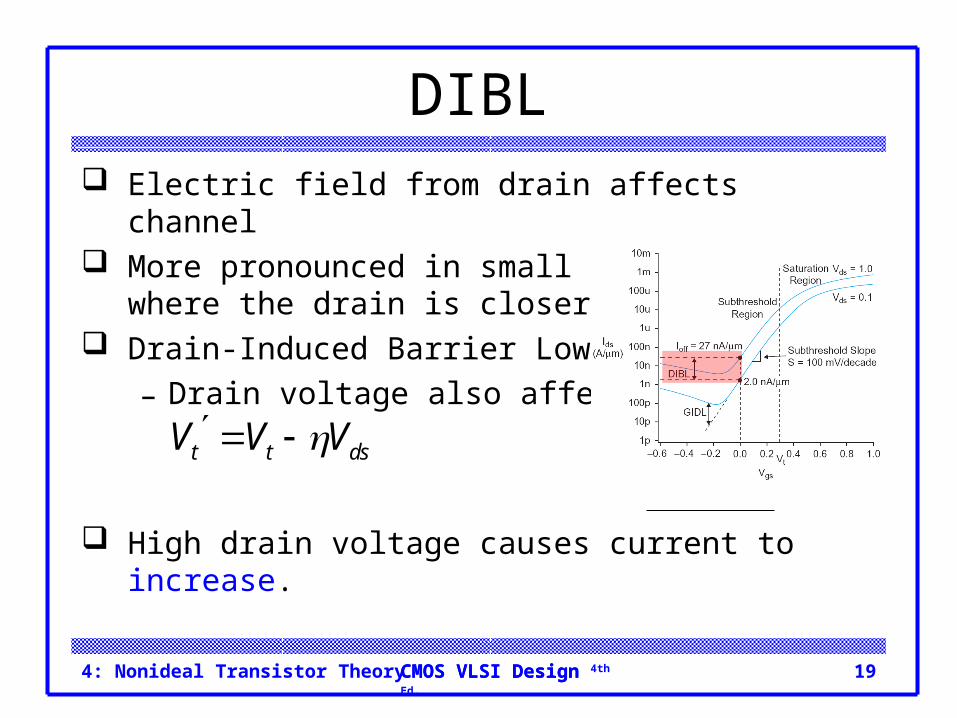
DIBL Electric field from drain affects channel More pronounced in small transistors where the
drain is closer to the channel Drain-Induced Barrier Lowering
– Drain voltage also affect Vt
High drain voltage causes current to increase.
ttdsVVV
t t dsV V V
4: Nonideal Transistor Theory 20CMOS VLSI DesignCMOS VLSI Design 4th Ed.
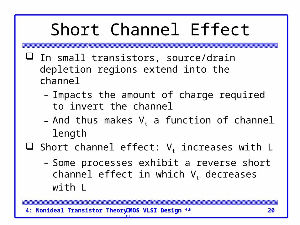
Short Channel Effect
In small transistors, source/drain depletion regions extend into the channel– Impacts the amount of charge required to invert
the channel
– And thus makes Vt a function of channel length
Short channel effect: Vt increases with L
– Some processes exhibit a reverse short channel effect in which Vt decreases with L
4: Nonideal Transistor Theory 21CMOS VLSI DesignCMOS VLSI Design 4th Ed.
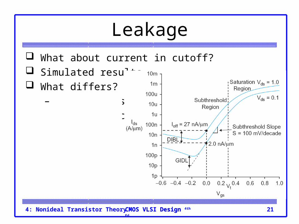
Leakage What about current in cutoff? Simulated results What differs?
– Current doesn’t
go to 0 in cutoff
4: Nonideal Transistor Theory 22CMOS VLSI DesignCMOS VLSI Design 4th Ed.
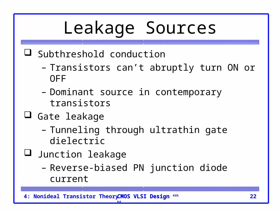
Leakage Sources Subthreshold conduction
– Transistors can’t abruptly turn ON or OFF– Dominant source in contemporary transistors
Gate leakage– Tunneling through ultrathin gate dielectric
Junction leakage– Reverse-biased PN junction diode current
4: Nonideal Transistor Theory 23CMOS VLSI DesignCMOS VLSI Design 4th Ed.
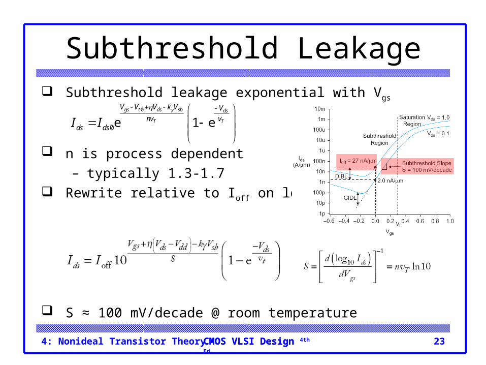
Subthreshold Leakage Subthreshold leakage exponential with Vgs
n is process dependent– typically 1.3-1.7
Rewrite relative to Ioff on log scale
S ≈ 100 mV/decade @ room temperature
0
0e 1 egs t ds sb ds
T T
V V V k V V
nv vds dsI I

4: Nonideal Transistor Theory 24CMOS VLSI DesignCMOS VLSI Design 4th Ed.
Gate Leakage Carriers tunnel through very thin gate oxides Exponentially sensitive to tox and VDD
– A and B are tech constants– Greater for electrons
• So nMOS gates leak more Negligible for older processes (tox > 20 Å)
Critically important at 65 nm and below (tox ≈ 10.5 Å)
From [Song01]
4: Nonideal Transistor Theory 25CMOS VLSI DesignCMOS VLSI Design 4th Ed.
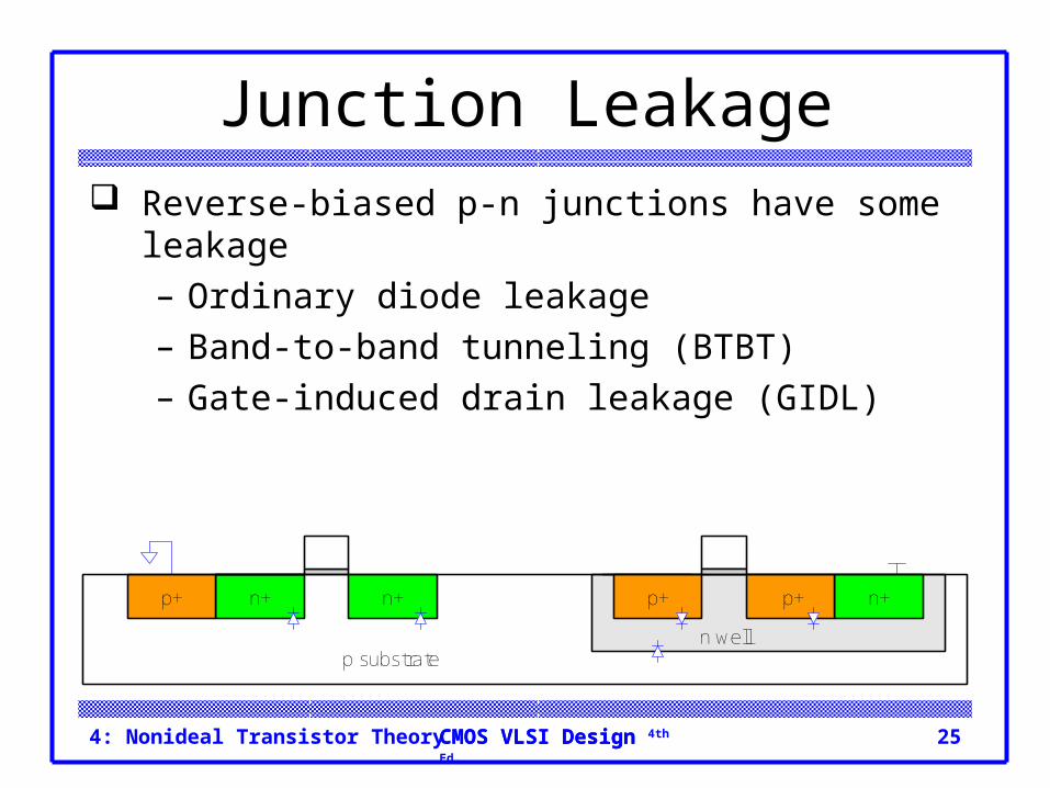
Junction Leakage Reverse-biased p-n junctions have some leakage
– Ordinary diode leakage– Band-to-band tunneling (BTBT)– Gate-induced drain leakage (GIDL)
n well
n+n+ n+p+p+p+
p substrate
4: Nonideal Transistor Theory 26CMOS VLSI DesignCMOS VLSI Design 4th Ed.
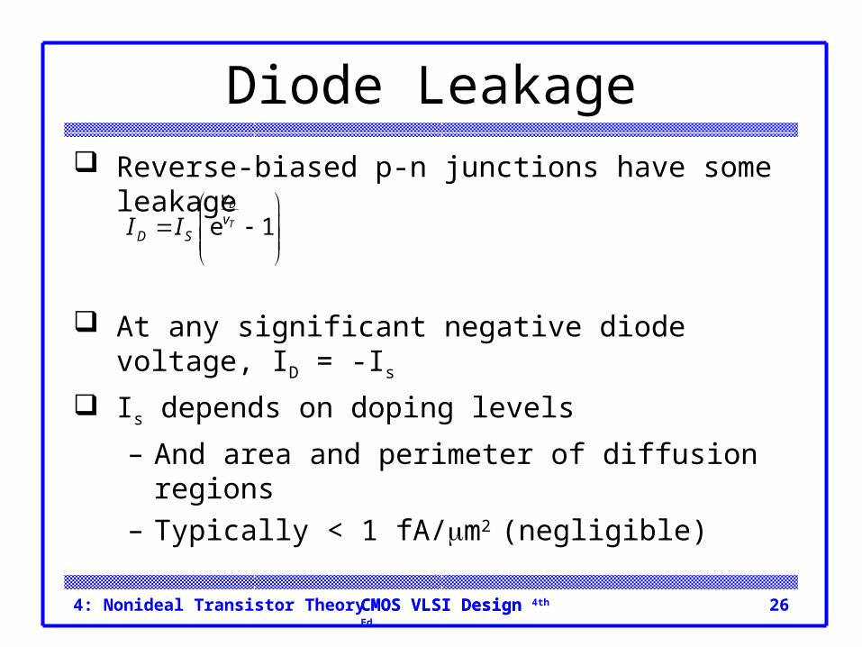
Diode Leakage Reverse-biased p-n junctions have some leakage
At any significant negative diode voltage, ID = -Is
Is depends on doping levels
– And area and perimeter of diffusion regions– Typically < 1 fA/m2 (negligible)
e 1D
T
V
vD SI I
4: Nonideal Transistor Theory 27CMOS VLSI DesignCMOS VLSI Design 4th Ed.
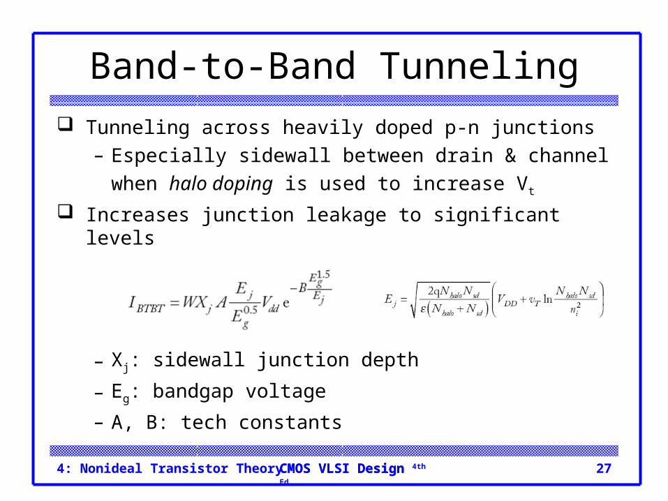
Band-to-Band Tunneling
Tunneling across heavily doped p-n junctions– Especially sidewall between drain & channel
when halo doping is used to increase Vt
Increases junction leakage to significant levels
– Xj: sidewall junction depth
– Eg: bandgap voltage
– A, B: tech constants
4: Nonideal Transistor Theory 28CMOS VLSI DesignCMOS VLSI Design 4th Ed.
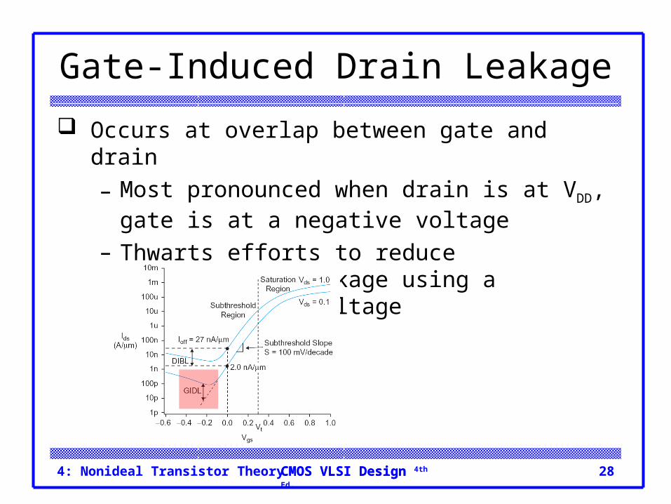
Gate-Induced Drain Leakage
Occurs at overlap between gate and drain
– Most pronounced when drain is at VDD, gate is at a negative voltage
– Thwarts efforts to reduce subthreshold leakage using a negative gate voltage
4: Nonideal Transistor Theory 29CMOS VLSI DesignCMOS VLSI Design 4th Ed.
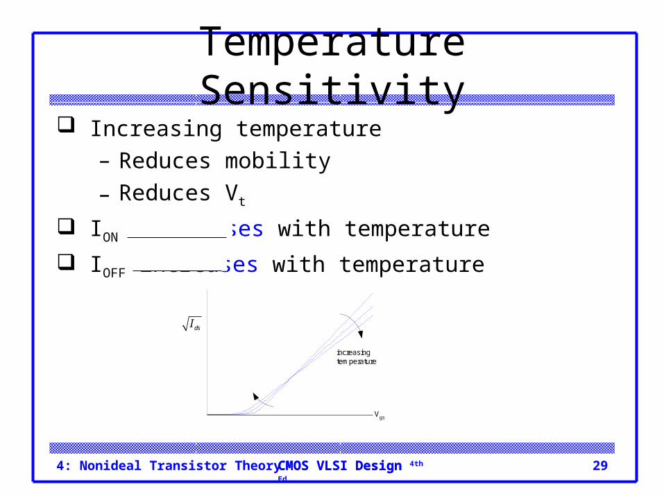
Temperature Sensitivity Increasing temperature
– Reduces mobility
– Reduces Vt
ION decreases with temperature
IOFF increases with temperature
Vgs
dsI
increasingtemperature
4: Nonideal Transistor Theory 30CMOS VLSI DesignCMOS VLSI Design 4th Ed.
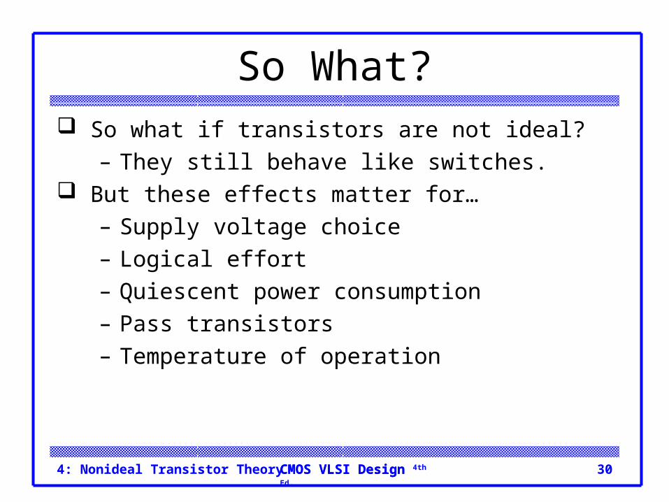
So What? So what if transistors are not ideal?
– They still behave like switches. But these effects matter for…
– Supply voltage choice– Logical effort– Quiescent power consumption– Pass transistors– Temperature of operation
4: Nonideal Transistor Theory 31CMOS VLSI DesignCMOS VLSI Design 4th Ed.
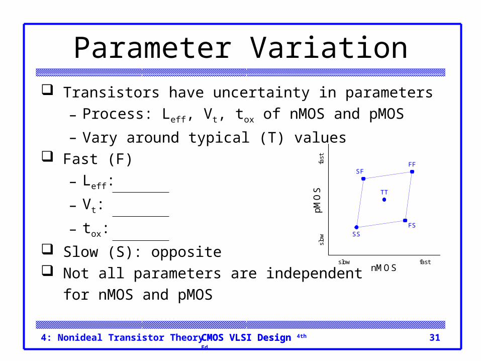
Parameter Variation Transistors have uncertainty in parameters
– Process: Leff, Vt, tox of nMOS and pMOS
– Vary around typical (T) values Fast (F)
– Leff: short
– Vt: low
– tox: thin
Slow (S): opposite Not all parameters are independent
for nMOS and pMOS
nMOS
pM
OS
fastslow
slow
fast
TT
FF
SS
FS
SF
4: Nonideal Transistor Theory 32CMOS VLSI DesignCMOS VLSI Design 4th Ed.
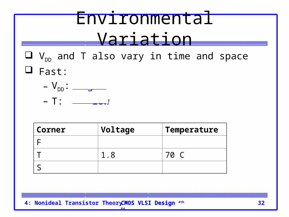
Environmental Variation VDD and T also vary in time and space
Fast:
– VDD: high
– T: low
Corner Voltage Temperature
F 1.98 0 C
T 1.8 70 C
S 1.62 125 C
4: Nonideal Transistor Theory 33CMOS VLSI DesignCMOS VLSI Design 4th Ed.
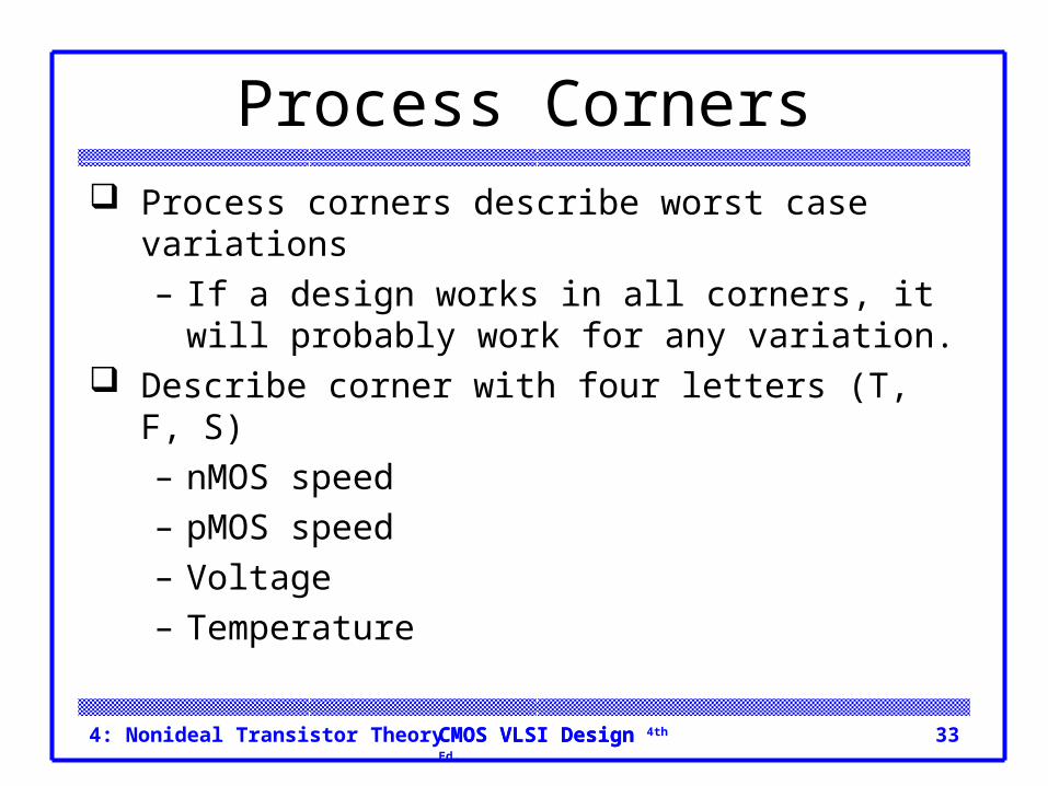
Process Corners Process corners describe worst case variations
– If a design works in all corners, it will probably work for any variation.
Describe corner with four letters (T, F, S)– nMOS speed– pMOS speed– Voltage– Temperature
4: Nonideal Transistor Theory 34CMOS VLSI DesignCMOS VLSI Design 4th Ed.
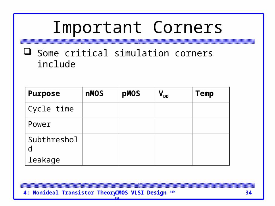
Important Corners Some critical simulation corners include
Purpose nMOS pMOS VDD Temp
Cycle time S S S S
Power F F F F
Subthreshold
leakage
F F F S
4: Nonideal Transistor Theory 35CMOS VLSI DesignCMOS VLSI Design 4th Ed.
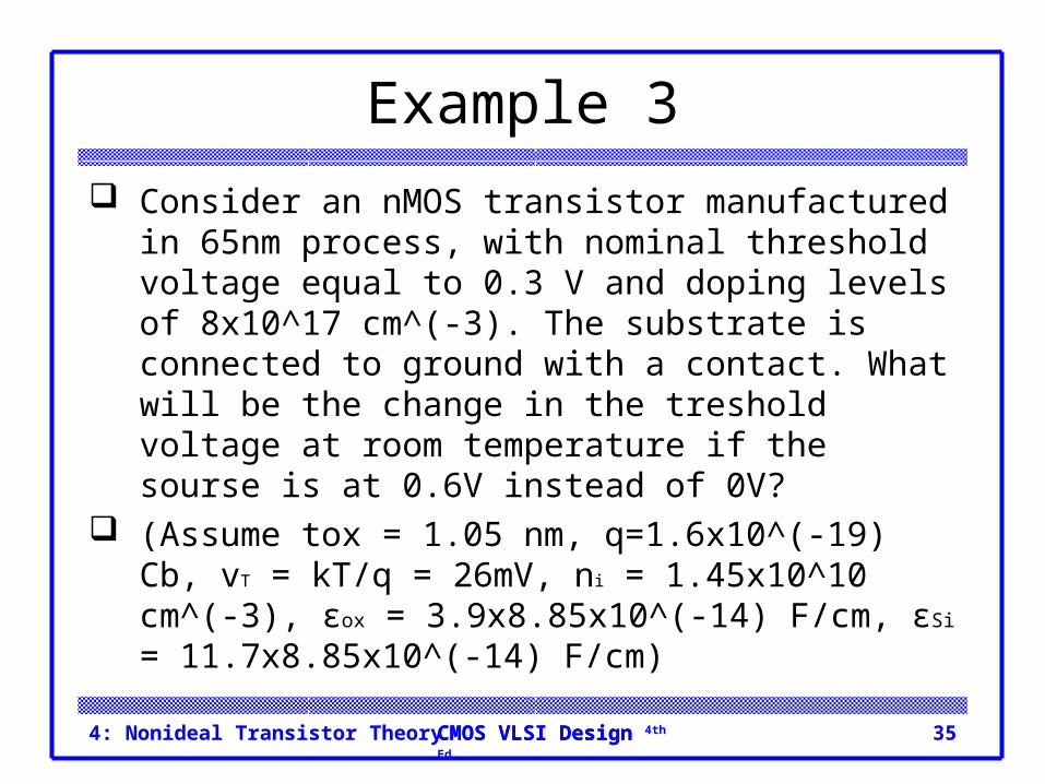
Example 3
Consider an nMOS transistor manufactured in 65nm process, with nominal threshold voltage equal to 0.3 V and doping levels of 8x10^17 cm^(-3). The substrate is connected to ground with a contact. What will be the change in the treshold voltage at room temperature if the sourse is at 0.6V instead of 0V?
(Assume tox = 1.05 nm, q=1.6x10^(-19) Cb, vT = kT/q = 26mV, ni = 1.45x10^10 cm^(-3), εox = 3.9x8.85x10^(-14) F/cm, εSi = 11.7x8.85x10^(-14) F/cm)
4: Nonideal Transistor Theory 36CMOS VLSI DesignCMOS VLSI Design 4th Ed.
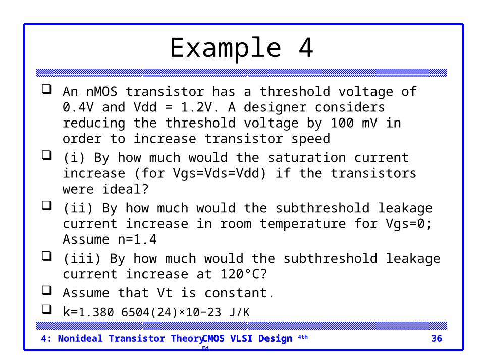
Example 4 An nMOS transistor has a threshold voltage of 0.4V and
Vdd = 1.2V. A designer considers reducing the threshold voltage by 100 mV in order to increase transistor speed
(i) By how much would the saturation current increase (for Vgs=Vds=Vdd) if the transistors were ideal?
(ii) By how much would the subthreshold leakage current increase in room temperature for Vgs=0; Assume n=1.4
(iii) By how much would the subthreshold leakage current increase at 120°C?
Assume that Vt is constant. k=1.380 6504(24)×10−23 J/K
4: Nonideal Transistor Theory 37CMOS VLSI DesignCMOS VLSI Design 4th Ed.
Example 5
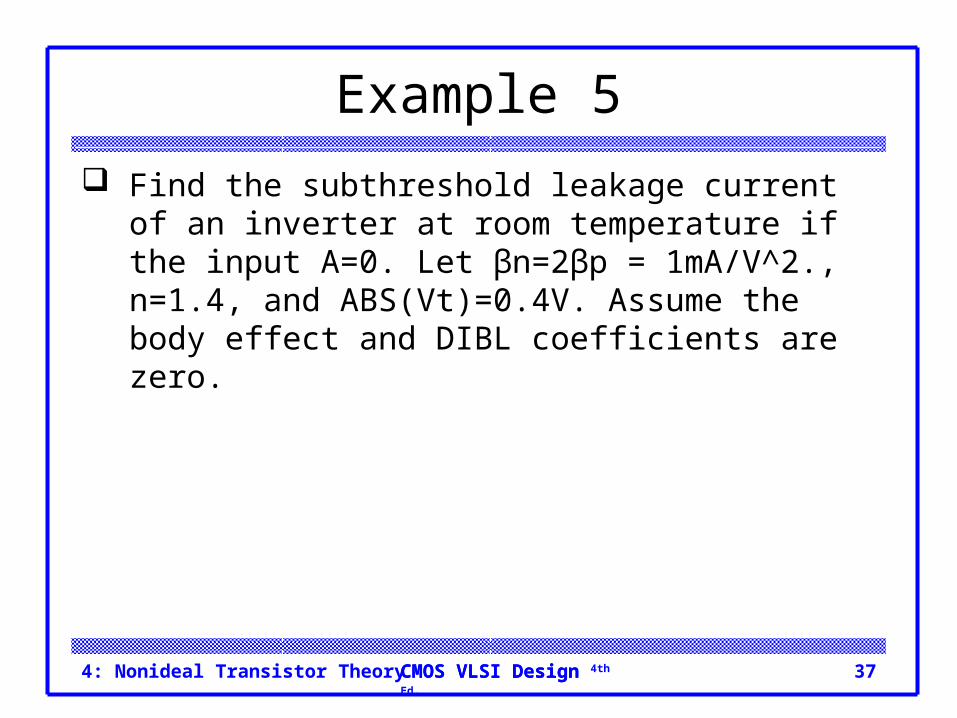
Find the subthreshold leakage current of an inverter at room temperature if the input A=0. Let βn=2βp = 1mA/V^2., n=1.4, and ABS(Vt)=0.4V. Assume the body effect and DIBL coefficients are zero.


