1 Lecture 38 Establishing DCM V out / V in Quadratic Relations A. DCM DC Transfer Functions via Quadratic Relations 1. Overview of the DCM Operation Conditions 2. V o for the Buck 3. V o for the Boost 4. V o for the Buck-Boost 5. Summary 6. L critical for the Three Major Circuits 7. Critical Capacitance: C critical B. Homework Solutions and Hints 1. Problem 5.1 2. Problem 5.9 3. Hints for Problem 5.4 4. Hints for Problem 5.14
A. DCM DC Transfer Functions via QuadraticRelations1. Overview of the DCM Operation Conditions2. Vo for the Buck3. Vo for the Boost4. Vo for the Buck-Boost5. Summary6. Lcritical for the Three Major Circuits7. Critical Capacitance: Ccritical
B. Homework Solutions and Hints1. Problem 5.12. Problem 5.93. Hints for Problem 5.44. Hints for Problem 5.14
A. DCM DC Transfer Functions via QuadraticRelations
1. OverviewThe figure below summarizes DCM operation for all threemajor converters: buck, boost and buck-boost usingtransistor and diode switches. Note IL(inductor) goes to zeroeach switch period and hence is insured to start form zero atthe start of each switch period. We will show iL(on far left),iin(middle plot), and id(far right) for each circuit versus time.Note that Vo in DCM comes only from solving a quadraticequation not from M(D), assuming Vin is constant over theswitch period. Pin = Pout is also assumed. We will use linearvariations of all currents as a good first approximation.
.1. Vo Buck
The three circuit topologies for the buck are as above:
3
The circuit and associated waveforms are shown below inDCM operation.
b. Derivation of DCM DC Transfer FunctionSince D1Ts is set by the control circuit and Vin is assumedconstant, the peak inductor current is from the far leftwaveform:
iL(peak) = ( )D TV V
L1 sin out−
From iin triangular waveforms in the middle plot we calculate:
Iin(av) = ( )D2
i (peak) = D TV V
2L1
L 12
sin out−
Pin(av) = Vin(constant)Iin(av) = ( )
D TV V V
2L12
sin
2in out−
For lossless converters we can say the following:Pin = Pout = V2
out/RYielding a quadratic equation in Vout.Solving:
Vo(DCM Buck) = - D V RT4L
+ D VRT2L
R T D16L
12
in s1 in
2s2
12
2+
4
c. Alternative Derivation
We get this from doing out steady-state balance. Theresulting plot for the buck DCM transfer function vs. D is:
Again note the trend for the DCM DC transfer function to bebigger for all D values than the CCM transfer function.3 .Vo Boost in DCM Operation
a. GeneralThe three circuit topologies for the DCM boost are shownbelow:
5
b. Derive DCM DC Transfer FunctionWe also show below the three boost circuit currentwaveforms IL(inductor),It(switch) and iD(diode):
b. Derive the DCM DC Transfer FunctionSince D1 is known and Vin is constant the peak inductorcurrent when the Tr is on is:
iL(peak) = D T VL
1 s in
From the sawtooth iin(t) waveform:
Iin(av) = D2
i (peak)1L = V D T
2Lin 1
2s
Pin(av) = Vin(const)Iin(av) = V D T2L
in2
12
s = Pout = Vo2/R
Solving for Vout directly:
Vo(Buck-Boost DCM) = - D VRT2L1 in
s
c. Alternative derivationFor HW# 2 YOU Derive the buck-boost transferfunction using the proper balance equationsDCM operation occurs for small L, L < Lc(critical), iL goes tozero before the end of the cycle and when the Tr goes on iLalways starts from zero. That is the ratio RTs/L has to bebelow a critical level to avoid DCM and remain in CCMoperation.
5. A summary would include:
This could also be plotted as shown below:
9
Next we get expressions for Lc(critical) for each convertertopology.
6. Lc(critical) for the Three Major Circuits
We expose the DCM / CCM boundary in terms of anLc(critical). When L = Lc the iL waveform is always triangularwithin Ts, so that D1 + D2 = 1. At this value of L we can alsouse the DCM expressions for Vo. Setting the two Voexpressions equal sets Lc.a. Buck critical L
For Vo = D1Vin (at DCM-CCM boundary)
[ ]V DR
D T2L
V D Vin2
1 12
s
cin
21 in
2= −
Lc = ( )RT2
1 Ds1−
The buck circuit below provides 100W at 5V with a 48Vinput.
10
V
R = 0.25
5 V
L
R-
+
Ω
C∞
What is Lc? At the DCM-CCM boundary using Vout =D1Vin yields D1 = 5/48 and D2 = 43/48. Pav = 100implies Iout(av) = 20A and ∆ iL(peak) = 2Iav = 40A.
e = Lcdi/dt where dt = D110µs43 = Lc*40/(5*50/48) or Lc = 1.1 µH
For L < Lc DCM operation for L > Lc CCM operation.
b. Boost critical L
For Vo = Vin/(1-D1) (at DCM-CCM boundary)V
(1- D )V D T R
2LV
1 Din
2
12
in2
12
s
c
in2
1= +
−
Lc = ( )D RT2
1 D1 s1− 2
In the boost circuit below Vin = 48V, Vo = 200V,L = 15 µH and fsw = 50 kHz (Ts = 20 µs)
48 V
Vout = 200 V
Vout
L
R-
+C∞
What is load P(min) so that L > Lc? At the DCM / CCMboundary using Vout = Vin/(1-D1) yields D1 = 0.76 and D2= 0.24. When the Tr is on VL is 48V for a time dt =0.76*20 µs.
11
VL = Ldi/dtThe di range during this time is 2IL(av) = 2Iin(av)2IL(av) = di > 48*0.76*20 / 15 µs = 48.64The load power must be at least 48*48.6 / 2 = 1167 W.
c. Buck-Boost critical Lc
For Vo = D1Vin/(1-D1) (at DCM-CCM boundary)Likewise from the DCM relations
V2out = V D RT
2LV D(1- D )
in2
12
s
c
in2
12
12=
Lc = ( )RT2
1 Ds1− 2
The buck-boost circuit below has Vin = 24V, Vo = -12Vand provides 60 W on average.
24 V
R = 0.25
VoutL R-
+
Ω
C∞
5 A
Vout = -12 V
Find Lc vs. fsw. Iout(av) = 60/12 = 5A. For Vin = 24VIin(av) = 25A. Now IL = Io + ID = 7.5A provided we are inCCM andL > Lc. Then iL is a triangle wave from 0 to 2. Iav = 15Aover the time D1Ts. Again Vo = VinD1 / (1-D1) yields D1 =1/3.
Lc(1kHz) = 533 µH but Lc(1MHz) = 0.5 µH. Clearlyhigher fsw is desired to make Lc as small as possible.
12
For HW#2 use the buck converter shown below:
V
R = 0.25
5 V
L
R-
+
Ω
C∞
A buck converter is designed for nominal 48 V inputand 5 V output. It switches at 100 KHz. In practice theinput can be anywhere between 30 V and 60 V. theload power ranges between 10 W and 200 W. What isLcrit for this converter? Conversely, what is themaximum inductance that will ensure discontinuousmode under all allowed conditions?
5. Critical Capacitance Cc(critical)
CCRITICAL is the capacitance required to keep Vc > 0 for allcircuit conditions. The Cuk circuit shown below has Vin =24V, Vo = -12, fsw = 200 kHz and provides 120 W.
24 V
Vout = -12 V
Vout
Lin
R-
+
C Lout
fswitch = 200 kHz
Lin, Lout ∞R = 1.2ΩWhat is Cc(critical)?Io(av) = 120/12 = 10A, RL = 1.2Ω , D1 = 1/3 and Iin(av) =120/24 = 5A. At the CCM / DCM boundary the boost portionprovides a voltage on average across the capacitor Vin/(1-D1) = 36V which is the sum of the input and output (12+24).
13
For Cc the Vc will vary from 0 to 2Vc(av) = 72V while thetransistor is on forD1Ts = (1/3)5 µs.
At Cc we get Vo = -12 for Vin = 24V. Will this Vo increase /decrease as C < Cc? What if C = Cc/2 = 0.116 µF?
Since we have DCM Vc will ramp down to zero while the Tris on. When Vc goes negative the diode goes on while theTr is on. This causes D1 + D2 > 1. While the diode is on fora time∆ t(1-D1)Ts = 3.33 µs. The voltage varies from 0 to 2(Vin+Vout).
Ic = Iin = Pin / Vin = C∆ V/∆ t
1. (Pin/Vin) = Cc*2(Vin + Vout)/3.33µs2. Pin = Pout = Vo
2/R
Combining 1. and 2. we obtain DCM:Vo
2 - 2Vo - 48 = 0Vout = 8VPout = Vo
2/1.6 = 53.33 WIin = 2.2A
Hence Vo drops for C < Cc
C. Homework Solutions and Hints1. Problem 5.1
Erickson Problem 5.1: Buck-boost is given on pages 14-16
14
15
2. Erickson Problem 5.9EMI Noise Issues from Converters to Mains: Example of
Input Filter PWM dc-dc buck converter
16
Erickson Problem. 5.9
17
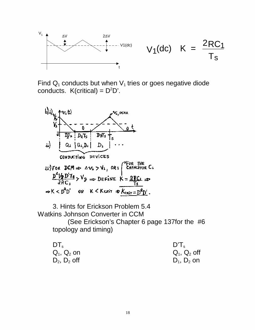
Now determine when the DCM occurs by plotting v1(t) withDC value and ripple
18
t
V1
V1(dc)
2∆ V∆ V
11
sV (dc) K = 2RC
T
Find Q1 conducts but when V1 tries or goes negative diodeconducts. K(critical) = D2D’.
3. Hints for Erickson Problem 5.4Watkins Johnson Converter in CCM
(See Erickson’s Chapter 6 page 137for the #6topology and timing)
DTs D’Ts
Q1, Q2 on Q1, Q2 offD2, D2 off D1, D2 on
19
VgVg
L
LC CR RVoVo
+
- -
IL
(Vg-Vo)/L
-Vg/L
Note: Be careful when dividing by a negative number. If youdivide by a negative number you must change the sign of theoperator ⇒ -5a < b or a > -b/5 but not a < -b/5, Try a=1 andb=1
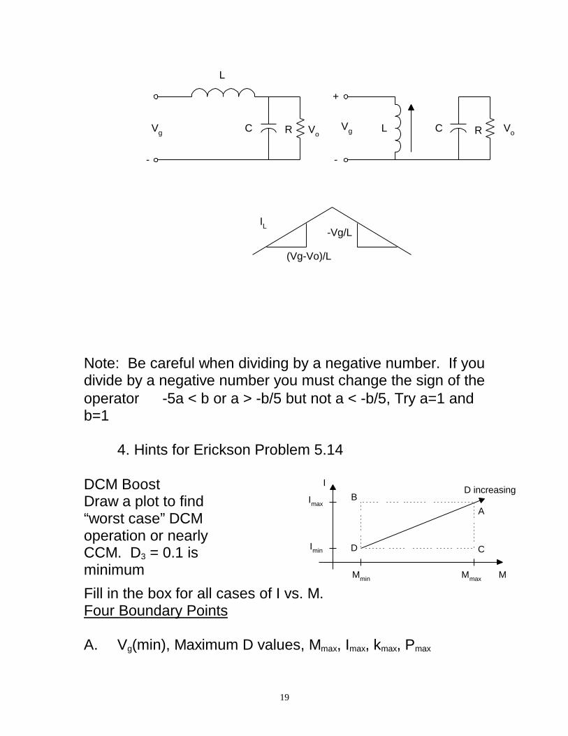
4. Hints for Erickson Problem 5.14
DCM BoostDraw a plot to find“worst case” DCMoperation or nearlyCCM. D3 = 0.1 isminimum
I
M
Imax
Imin
D increasing
AB
CD
Mmin Mmax
Fill in the box for all cases of I vs. M.Four Boundary Points
A. Vg(min), Maximum D values, Mmax, Imax, kmax, Pmax
20
Imax & Max D ⇒ worst caseD3 = 0.1 is lowest ≡ Point A
B. Vg(max), Mmin, Imax, kmax, Pmax
Intermediate D values
C. Vg(min), Intermediate D, Mmax, Imin, kmin, Pmin
D. Vg(max), Mmin, Imin, kmin, Pmin, Dmin
A is choice for boundary of CCM ↔ DCMand D3 = 0.1 at A as per statement in problem D3(min) = 0.