34
Lecture 6 Chapter 4.1 – 4.7

Lecture 6
Chapter 4.1 – 4.7

4.1 Introduction
• Digital systems consist of combinational and sequential circuits
– Combinational
• Operation specified logically by a set of Boolean functions
Outputs a function of inputs
– Sequential
• Outputs a function of inputs and state of storage elements

4.2 Combinational Circuits
• Combinational circuits consist of an interconnect of logic gates, configured to perform a given function
– For n inputs, there are 2n possible combinations
• Each output function is expressed in terms of the n inputs

4.3 Analysis Procedure
• The diagram of a combinational circuit has logic gates with no feedback paths or memory elements
– A feedback path is a connection from the output of gate to the input of a second gate whose output forms part of the input to the first gate

4.3 Analysis Procedure
• Analysis Steps: 1) Label all gate outputs that are a function of input
variables with arbitrary but meaningful names. Determine the Boolean functions for each gate output
2) Label the gates that are a function of input variables and previously labeled gates with other arbitrary symbols
3) Repeat the process outlined in step 2 until the outputs of the circuits are obtained
4) By repeating substitution of previously defined functions, obtain the output Boolean functions in terms of input variables

4.3 Analysis Procedure T2 = ABC
T1 = A + B +C
F2 = AB + AC + BC
T3 = F’2T1
F1 = T3 + T2
F1 = T3 + T2 = F’2T1 + ABC F1 = (AB + AC + BC)’(A + B + C) + ABC F1 = (A’ + B’)(A’ + C’)(B’ + C’)(A + B + C) + ABC F1 = (A’ B’C’)(AB’ + AC’ BC’ B’C) + ABC F1 = A’BC’ + A’B’C + AB’C’ ABC

4.3 Analysis Procedure
1

4.4 Design Procedure
• Combinational circuit design starts from the specification of the design objective and culminates in a logic circuit schematic or a set of Boolean functions which the logic circuit or RTL code can be obtained 1) From eh circuit specifications, determine the number of
inputs and outputs required and assign a symbol to each
2) Derive the truth table that defines the relationship required between inputs and outputs
3) Obtain the simplified Boolean functions for each output as a function of the input variables
4) Draw the logic diagram and/or code using RTL language and verify the design correctness

4.4 Design Procedure
• Code Conversion Example:
– Convert BCD to Excess-3 Code

4.4 Design Procedure
• Code Conversion Example (cont.):

4.4 Design Procedure
z = D’ y = CD + C’D’ = CD + (C + D)’ x = B’C + B’D + BC’D’ = B’(C +D) + BC’D’ = B’(C +D) + B(C +D)’ w = A + BC + BD = A + B( C +D)
4.5 Binary Adder-Subtractor
• Recall: 0 + 0 = 0 0 + 1 = 1 1 + 0 = 1 1 + 1 = 102 (Carry, Sum)
• A combinational circuit that performs addition of two bits is called a half adder
• A combinational circuit that performs addition of three bits (two significant bits and a previous carry) is called a full adder – Two half adder can be employed to implement a full adder
• A binary adder-subtractor is a combinational circuit that performs arithmetic operations of addition and subtraction with binary numbers

4.5 Binary Adder-Subtractor
• Half Adder:
Let Sum = S, Carry = C
Two inputs x, and y:
S = x’y + xy’
C = xy

4.5 Binary Adder-Subtractor
• Full Adder – A full adder is a comb. circuit that forms the arithmetic
sum of three bits • Two of the inputs variables, denoted by x and y, represent the two
significant bits to be added
• The third input, z, represents the carry from the previous lower significant positions
• The two outputs are designated S for Sum and C for Carry – S gives the least significant bit of the Sum
– C gives the carry formed by adding the input carry and the bits of the words
– The process of addition proceeds on a bit by bit basis, right to left, beginning with the least significant bit (LSB)

4.5 Binary Adder-Subtractor
• Binary Adder (cont.):
– From Table 4.4
S = x’y’z + x’yz’ + xy’z’ + xyz
C = xy + xz + yz
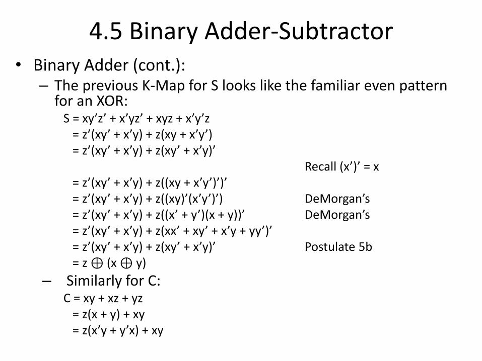
4.5 Binary Adder-Subtractor • Binary Adder (cont.):
– The previous K-Map for S looks like the familiar even pattern for an XOR:
S = xy’z’ + x’yz’ + xyz + x’y’z = z’(xy’ + x’y) + z(xy + x’y’) = z’(xy’ + x’y) + z(xy’ + x’y)’ Recall (x’)’ = x = z’(xy’ + x’y) + z((xy + x’y’)’)’ = z’(xy’ + x’y) + z((xy)’(x’y’)’) DeMorgan’s = z’(xy’ + x’y) + z((x’ + y’)(x + y))’ DeMorgan’s = z’(xy’ + x’y) + z(xx’ + xy’ + x’y + yy’)’ = z’(xy’ + x’y) + z(xy’ + x’y)’ Postulate 5b = z ⊕ (x ⊕ y)
– Similarly for C: C = xy + xz + yz = z(x + y) + xy = z(x’y + y’x) + xy

4.5 Binary Adder-Subtractor S = z ⊕ (x ⊕ y)
C = z(x ⊕ y) + xy

4.5 Binary Adder-Subtractor • The addition of n-bits requires a chain of n full
adders or a chain of one half adder and n-1 full adders
– Consider: A = 1011, B = 0011
Subscript i: 3 2 1 0
Input carry 0 1 1 0 Ci
Augend 1 0 1 1 Ai
Addend 0 0 1 1 Bi
Sum 1 1 1 0 Si
Carry 0 0 1 1 Ci+1

4.5 Binary Adder-Subtractor
• Carry Propagation:
• Daisy Chaining full adders results in long path for carry
– Ripple carry value dependent on all previous carries.
– Charles Babbage ( 1791 – 1871) recognized carry delay issue and devised anticipating carriage mechanisms for his devices.
– First patent filed in 1957 by IBM

4.5 Binary Adder-Subtractor
• Define two new binary variables:
Pi = Ai + Bi (Carry Propagate – Determines if a carry propagates)
Gi = AiBi (Carry Generate – produces carry when A = B = 1)
• The output sum and carry can be expressed as
Si = Pi + Ci
Ci+1 = Gi + PiCi
• Carry output Boolean functions: C0 = input carry
C1 = G0 + P0C0

4.5 Binary Adder-Subtractor • Carry Look Ahead (cont.)
• Four bit Adder Carry Output Boolean functions: C0 = input carry
C1 = G0 + P0C0
C2 = G1 + P1C1 = G1 + P1 (G0 + P0G0) = G1 + P1G0 + P1P0C0
C3 = G2 + P2C2 = G2 + P2G1 + P2P1G0 = P2P1P0C0
C1
C0
C1
P1
P0
G0
G1
+ P0C0
P1C1
+

4.5 Binary Adder-Subtractor • Carry Look Ahead (cont.) Four bit Adder Carry Output Boolean functions:
C0 = input carry
C1 = G0 + P0C0
C2 = G1 + P1C1 = G1 + P1 (G0 + P0G0) = G1 + P1G0 + P1P0C0
C3 = G2 + P2C2 = G2 + P2G1 + P2P1G0 = P2P1P0C0

4.5 Binary Adder-Subtractor
• Binary Subtrator
– As discussed in Section 1.5, the subtraction of binary numbers can be done by means of complements
• To subtract A – B, take 2’s complement of B and add to A
• 2’s complement is formed by taking the 1’s complement and adding 1 to the least significant pair of bits
• 1’s complement is formed by inverting value
• The 1 can be added to the sum via the carry input

4.5 Binary Adder-Subtractor • The addition and subtraction operations can be
combined into one circuit with one common binary adder including an exclusive – OR gate with each full adder:
Subtract: M = 1, C0 = 1, Bi ⊕ 1 = Bi’
Add: M = 0, C0 = 0, Bi ⊕ 0 = Bi

4.5 Binary Adder-Subtractor
• Overflow – An overflow occurs when the sum of two n digit
numbers occupies n + 1 digits
– The detection of an overflow depends on whether the numbers are considered to be signed or unsigned • Two unsigned overflow is detected from end carry out
of the most significant position
• For signed numbers: – The leftmost bit represents the sign (0 for +, 1 for -)
– Negative numbers are in 2’s complement form
– When the two numbers are added, the sign bit is treated as part of the number and the end carry does not indicate an overflow

4.5 Binary Adder-Subtractor
• Overflow (cont.):
– An overflow cannot occur after an addition if one number is positive and one is negative as the sum will always be less than the largest number
– An overflow can occur if both numbers are either positive or negative
– An overflow can be detected by observing the carry into the sign bit position and the carry out of the sign bit position
• If these two carries are not equal, an overflow has occurred
• Apply the two carries to an XOR to detect

4.5 Binary Adder-Subtractor
• Overflow (cont.):
carries: 0 1
+70 0 1000110
+80 0 1010000
+150 1 0010110
carries: 1 0
-70 1 0111010
-80 1 0110000
-150 0 1101010

4.6 Decimal Adder
• BCD Adder: – Recall that for BCD, the digit does not exceed 9
(1001)2, thus the output sum cannot be greater than 9 + 9 + 1 = 19 ( the 1 being an input carry)
– Recall from Chapter 1 that when the sum is <= 10012 (w/o a carry), the corresponding BCD digit is correct.
– When the sum is > 10012, the addition of 01102 to the binary sum converts it to the correct digit and produces a carry as well.

4.6 Decimal Adder
• Apply two BCD digits to a four bit binary adder
No conversion required
Need to add (0110)2 to Binary Sum
C = K + Z8Z4 + Z8Z2

4.6 Decimal Adder

4.7 Binary Multiplier • The multiplicand is multiplied by each bit of
the multiplier, starting with the LSB
• Each such multiplication forms a partial product
• The final product is obtained from the sum of the partial products – The multiplication of
Ai and Bi produce a 1 if both are 1;
otherwise it produces a 0 (AND operation)

4.7 Binary Multiplier

4.7 Binary Multiplier • Consider a multiplier that multiplies a binary number represented by four bits by a
number represented by three bit – Let the multiplicand be represented by B3B2B1B0
– Let the multiplier be represented by A2A1A0
B3 B2 B1 B0
A2 A1 A0
A0B3 A0B2 A0B1 A0B0
A1B3 A1B2 A1B1 A1B0
A2B3 A2B2 A2B1 A2B0
C6 C5 C4 C3 C2 C1 C0
A0B0 A0B1 A0B2 A0B3
A0B1 + A1B0

Homework
• For the full adder on page 136, show
C = xy + xz + yz = z(xy’ + x’y) using the Postulates and Theorems from Table 2.1 (10 points)
• 4.1 a-c (10 pts. ea.)
• 4.49 a-b (20 pts. ea.)


