(c) Dr. Sajid M Choudhury. Please do not redistribute or upload without prior permission. 3/9/20 1 Lecture-7 – Verilog for Logic Synthesis Dr. Sajid Muhaimin Choudhury Dept of EEE, BUET EEE 303 – Digital Electronics 1 3/9/20 2 2
Transcript
(c) Dr. Sajid M Choudhury. Please do not redistribute or upload without prior permission.
3/9/20
1
Lecture-7 – Verilog for Logic Synthesis
Dr. Sajid Muhaimin ChoudhuryDept of EEE, BUET
EEE 303 – Digital Electronics
1
3/9/20 2
2
(c) Dr. Sajid M Choudhury. Please do not redistribute or upload without prior permission.
3/9/20
2
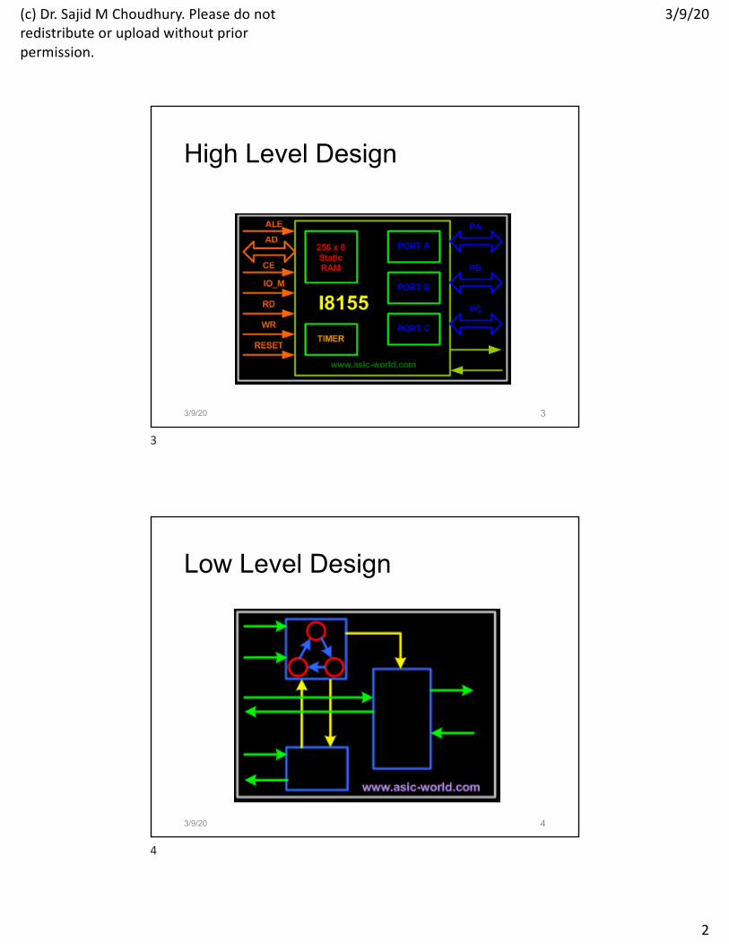
High Level Design
3/9/20 3
3
Low Level Design
3/9/20 4
4
(c) Dr. Sajid M Choudhury. Please do not redistribute or upload without prior permission.
3/9/20
3
RTL Coding
• Register Transfer Logic• Micro design is converted into Verilog/VHDL code, using synthesizable constructs of the language.
3/9/20 5
5
Verilog Module
• An elementary Verilog program is called a module. • A module corresponds to a digital circuit.
Modules have input and output ports that correspond to the input
• and output terminals of a digital circuit. • The ports and variables used to represent internal
signals are declared at the beginning of the program.
• Modules have other statements used to define how it transforms the input signals to output signals.
3/5/20 6
6
(c) Dr. Sajid M Choudhury. Please do not redistribute or upload without prior permission.
3/9/20
4
Structural vs Behavior
• Structural modules consist of a list of component modules (defined elsewhere) and a list of wires used to interconnect the modules.
• Behavior modules specify the output signals as functions of the input signals. They need not give any indication of the structure of the circuit.
3/5/20 7
7
Example of a behavioral Verilog module • Circuit:
• Verilog module: module circuit1b (A, B, C, D, E, X, Y, Z); input A, B, C, D, E; output X, Y, Z;assign X = ~((A ^ B) | C); assign Y = ~((B & C) | D) & E;assign Z = A | D | (B & C); endmodule
3/5/20 8
8
(c) Dr. Sajid M Choudhury. Please do not redistribute or upload without prior permission.
3/9/20
5
Verilog Input and Output• Individual signals (e.g., A, B, ... in the previous example) can
take any of the following four values: • 0 = logic value 0
1 = logic value 1z = tri-state (high impedance) x = unknown value
• The unknown value is used by simulators to indicate that they do not know how to determine a signals value (e.g., the user has not specified a value for an input signal). The tri-state value means that no signal is assigned to the variable.
• The unknown value x can also be used to specify a don’t care condition to the synthesis tools.
• Note that ports must be listed in the module statement (first line) and their direction (input or output) declared in the following statements.
3/5/20 9
9
• The three assign statements are independent and can execute in any order or concurrently.
• The right side of an assign statement is evaluated and its resulting value assigned to the signal on the left side whenever one of the signals used in the right side changes value.
• This type of assignment is also called a continuous assignment. • This method of interpreting the execution of assign statements is quite
different • from that use in conventional programming languages in the following
ways: • Two or more assignments can execute simultaneously. This is
necessary to represent the timing characteristics of hardware systems. • An assignment executes whenever it is ready (i.e., has new data for
the variables on its right side) • There is no concept of "locus of control" or “program counter” that
determines the next instruction to execute. Therefore, the order the assignments are written does not matter
• This method of assignment statement execution is sometimes called non-procedural or data-driven execution, where conventional programming languages are said to be procedural.
3/5/20 10
10
(c) Dr. Sajid M Choudhury. Please do not redistribute or upload without prior permission.
3/9/20
6
Behavioral vs. Structural Verilog Descriptions
• The previous example is a behavioral descriptions because it specifies the logical values of the circuit's outputs as logical equations with no reference to how the gates in a possible implementation might be interconnected.
• It is also possible to specify a structural description in Verilog that specifies explicitly how a set of smaller components (e.g., gates) are interconnected to form a larger system as shown on the following slide.
• Note that the internal connections from gate outputs to gate inputs are declared to be of type wire.
• These wire declarations could be omitted as long as the component modules are simple gates. Verilog will assume that any gate output signal that is not declared is of type wire.
• Each gate is specified by its name (e.g., and, or, ...) and a list of ports or wires connected to its terminals. All gates have a single output and it is always listed first in this list.
3/5/20 11
11
Structural Verilogmodule circuit1s (A, B, C, D, E, X, Y, Z); input A, B, C, D, E;output X, Y, Z;wire T1, T2, T3, T4, T5, T6, T7; xor(T1, A, B); or(T2,T1,C);not(X, T2); and(T3, B, C); or(T4, T3, D); not(T5, T4); and(Y, T5, E);or(T6, A, D); and(T7, B, C); or(Z, T6, T7); endmodule
3/5/20 12
12
(c) Dr. Sajid M Choudhury. Please do not redistribute or upload without prior permission.
3/9/20
7
Procedural Block (Always Blocks)• A procedural block is a construct that contains
statements that are executed procedurally (i.e., in the order they are written).always @(sensitivity_list)
begin procedural statements end
• The sensitivity list is a list of signals separated by or. • When any one of the signals in the sensitivity list changes
value, the always block wakes up, executes its procedural statements, and then goes back to sleep.
• The always block acts like a generalized assign statement where the action that takes place can be specified by sequential code.
3/5/20 13
13
Always Block Example
module always_example(x, y, z);input x, y;output z; reg z, s;always @(x or y) begin
s = x ^ y;z = x & s;
end endmodule
3/5/20 14
14
(c) Dr. Sajid M Choudhury. Please do not redistribute or upload without prior permission.
3/9/20
8
Reg variable• Variables declared as type reg hold their value until they
are assigned a new value. It is said that the assigned value is registered in the variable
• Whenever x or y changes value, the always block is executed as follows:
• First, the statement s = x^y executes and registers a new value in s Next, the statement z = x & s executes using the new value of s that
• it received when the first statement was executed. • Then the block stops executing and waits for either x or y to change
again.
• Variables on the left side of a procedural statement must be declared as type reg.
• The main advantage of using always blocks to represent combinational circuits is that you can use control statements such as “if then else” as illustrated by the following example
3/5/20 15
15
Explain how the behaviors of the following two modules differ
3/5/20 16
16
(c) Dr. Sajid M Choudhury. Please do not redistribute or upload without prior permission.
3/9/20
9
Conditions for combinational behavior of always blocks • The following conditions are necessary for an always block to
represent combinational logic (as opposed to sequential logic)
• All reg, wire and input signals that appear on the right side of an assignment statement within the always block must appear in the sensitivity list
• We call a sensitivity list that satisfies this condition a complete sensitivity list. • All signals in the sensitivity list must appear without edge specifiers
• Edge specifiers indicate that a signal is asserted by a change in value as opposed to its level (e.g., a rising edge or falling edge). They are introduced and utilized in later chapters on sequential circuits.
• All output signals must be assigned a value every time the always block executes
• These conditions guarantee that the input signals uniquely determine the output signals, which is the very definition of a combinational circuit.
• A sensitivity list of the form @(*) is shorthand for a complete list. It is recommended that you use this notation for combinational always block 3/5/20 17
17
Example (Incomplete sensitivity list)
module example1(a, b, c, f); input a, b, c; output f;reg f; always @(a, b)
if (a==1) f = b;
else f = c;
3/5/20 18
18
(c) Dr. Sajid M Choudhury. Please do not redistribute or upload without prior permission.
3/9/20
10
Logic Operation
3/9/20 19
19
Examples
• a = b + c ; • a = 1 << 5; • a = !b ;• a = ~b ;
3/9/20 20
20
(c) Dr. Sajid M Choudhury. Please do not redistribute or upload without prior permission.
3/9/20
11
If-else-end
3/9/20 21
21
Case
3/9/20 22
It's a good idea to have a default case. If the Verilog machine enters into a non-covered statement, the machine hangs. Defaulting the statement with a return to idle keeps us safe.
22
(c) Dr. Sajid M Choudhury. Please do not redistribute or upload without prior permission.
3/9/20
12
WhileA while statement executes the code within it repeatedly if the condition it is assigned to check returns true.
3/9/20 23
23
While - counter
3/9/20 24
24
(c) Dr. Sajid M Choudhury. Please do not redistribute or upload without prior permission.
3/9/20
13
For
3/9/20 25
25
Initial Block• An initial block, as the name suggests, is
executed only once when simulation starts. This is useful in writing test benches.
3/9/20 26
26
(c) Dr. Sajid M Choudhury. Please do not redistribute or upload without prior permission.
3/9/20
14
Lecture-8 – Combinational Logic
Dr. Sajid Muhaimin ChoudhuryDept of EEE, BUET
EEE 303 – Digital Electronics
27
3/5/20 28
28
(c) Dr. Sajid M Choudhury. Please do not redistribute or upload without prior permission.
3/9/20
15
Inverted Logic: SOP vs POS
3/9/20 29
29
Universal Gates
• NAND• NOR
3/5/20 30
30
(c) Dr. Sajid M Choudhury. Please do not redistribute or upload without prior permission.
3/9/20
16
NAND as Universal Gate
3/5/20 31
31
• Implement the following function with NAND logic only:
• X = AB + CD
3/5/20 32
32
(c) Dr. Sajid M Choudhury. Please do not redistribute or upload without prior permission.
3/9/20
17
X=AB+CD
3/5/20 33
33
NAND Implementation
3/5/20 34
34
(c) Dr. Sajid M Choudhury. Please do not redistribute or upload without prior permission.
3/9/20
18
NAND to AND-OR logic
3/5/20 35
35
Dual Symbols
36
(c) Dr. Sajid M Choudhury. Please do not redistribute or upload without prior permission.
3/9/20
19
NAND with Dual Symbols• All logic diagrams using NAND gates should be
drawn with each gate represented by either a NAND symbol or the equivalent negative-OR symbol to reflect the operation of the gate within the logic circuit.
• The NAND symbol and the negative-OR symbol are called dual symbols.
• When drawing a NAND logic diagram, choose gate symbols in a way that every connection between a gate output and a gate input is either bubble-to- bubble or nonbubble-to-nonbubble.
3/5/20 37
37
3/5/20 38
38
(c) Dr. Sajid M Choudhury. Please do not redistribute or upload without prior permission.
3/9/20
20
Dual Symbol Representation
3/5/20 39
39
NOR as Universal Gate
3/5/20 40
40
(c) Dr. Sajid M Choudhury. Please do not redistribute or upload without prior permission.
3/9/20
21
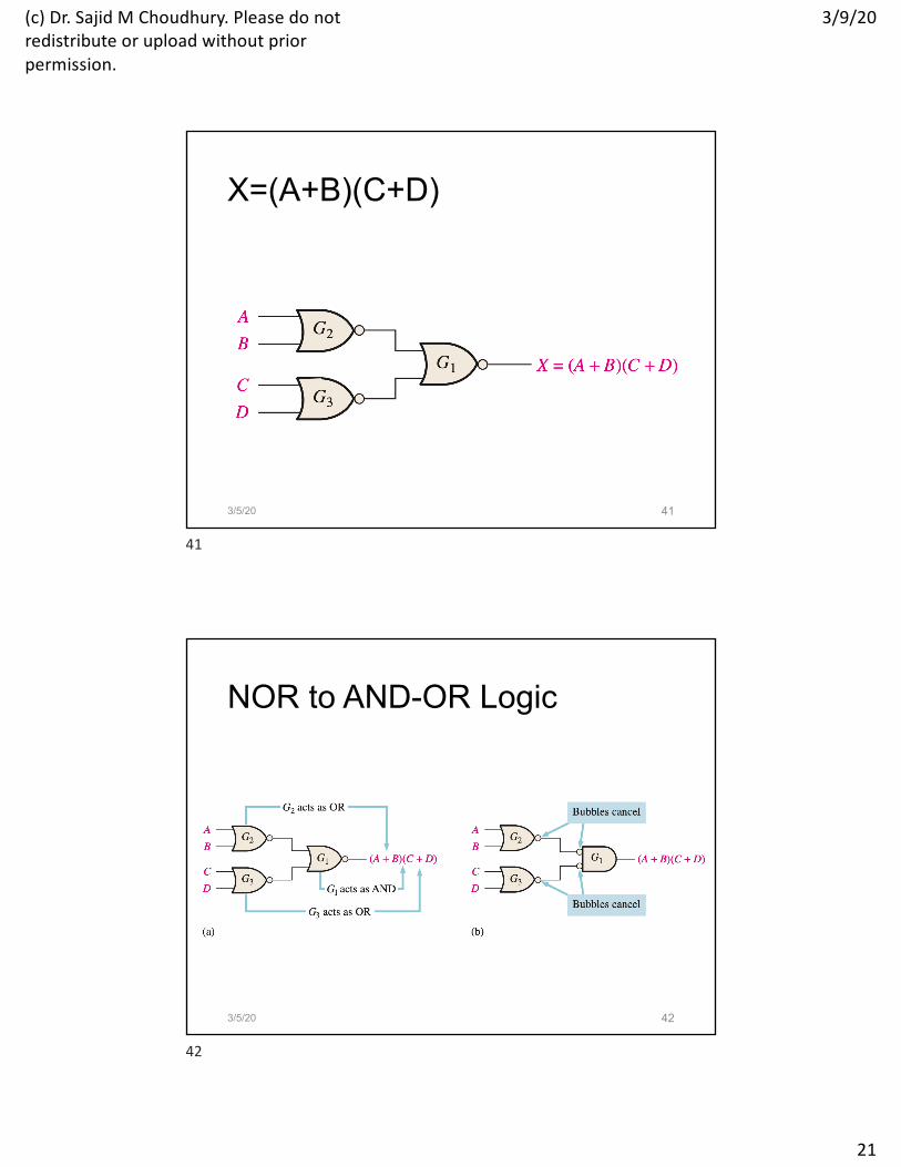
X=(A+B)(C+D)
3/5/20 41
41
NOR to AND-OR Logic
3/5/20 42
42
(c) Dr. Sajid M Choudhury. Please do not redistribute or upload without prior permission.