40
LECTURE 8: OSCILLATORS NOISE IN ELECTRONIC SYSTEMS
LECTURE 8:
OSCILLATORS
NOISE IN ELECTRONIC SYSTEMS

Oscillators
Wien-Bridge
Relaxation Oscillator
Noise Noise
Type of Noise
Noise Sources
OSCILLATORS
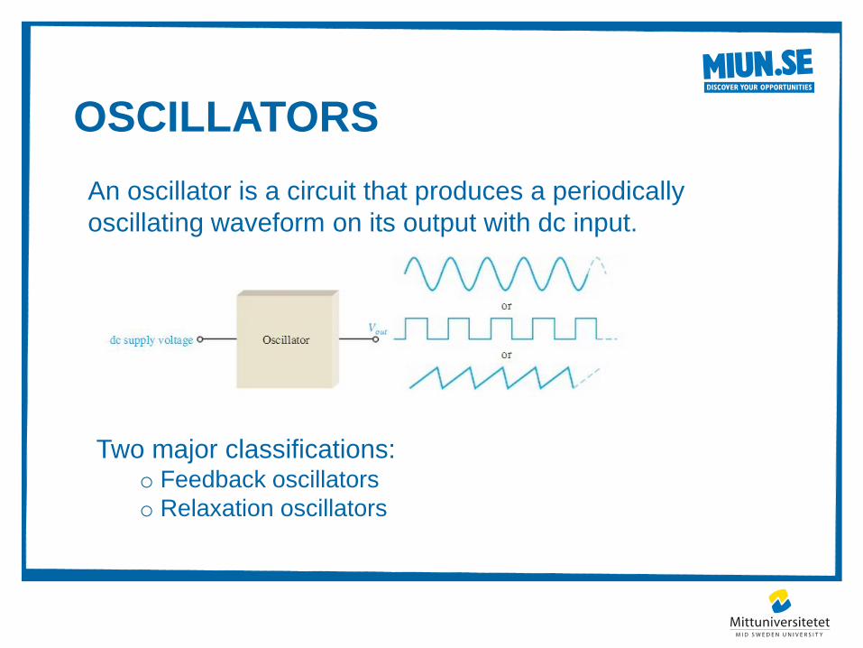
An oscillator is a circuit that produces a periodically
oscillating waveform on its output with dc input.
Two major classifications: o Feedback oscillators
o Relaxation oscillators
FEEDBACK OSCILLATORS
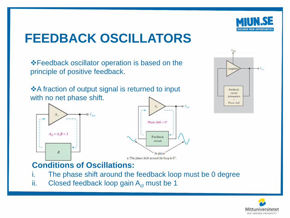
Feedback oscillator operation is based on the
principle of positive feedback.
A fraction of output signal is returned to input
with no net phase shift.
Conditions of Oscillations: i. The phase shift around the feedback loop must be 0 degree
ii. Closed feedback loop gain Acl must be 1
FEEDBACK OSCILLATORS
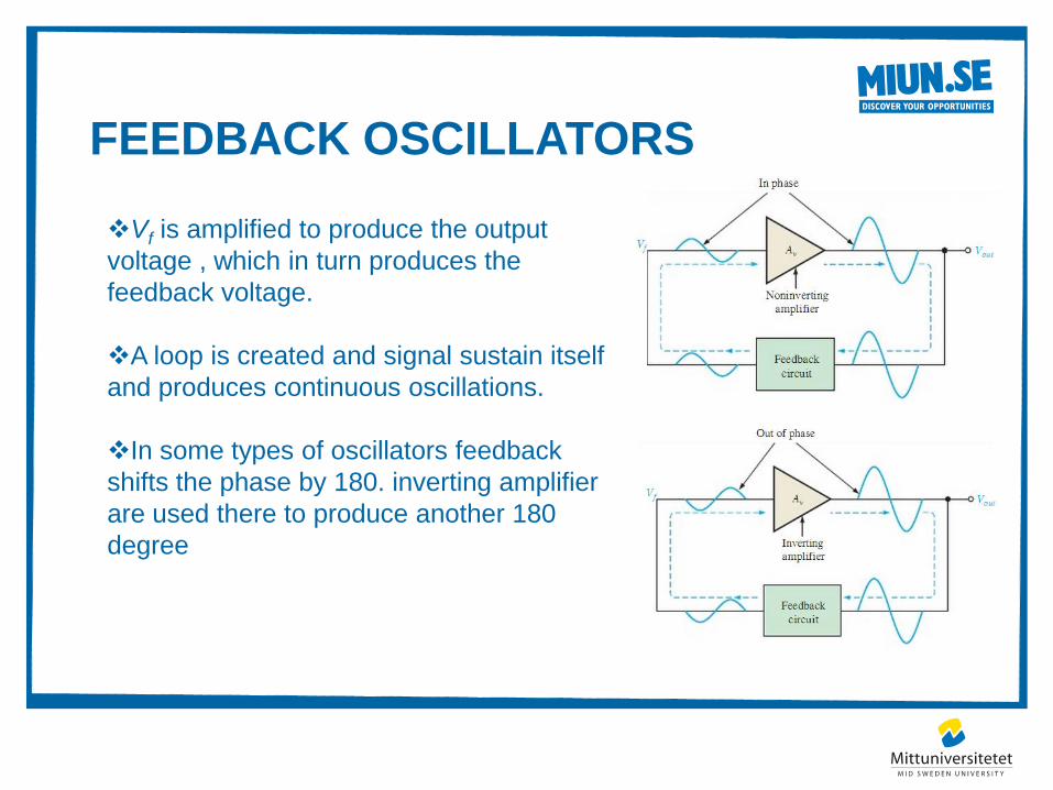
Vf is amplified to produce the output
voltage , which in turn produces the
feedback voltage.
A loop is created and signal sustain itself
and produces continuous oscillations.
In some types of oscillators feedback
shifts the phase by 180. inverting amplifier
are used there to produce another 180
degree
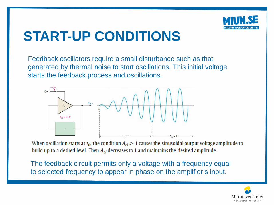
START-UP CONDITIONS
Feedback oscillators require a small disturbance such as that
generated by thermal noise to start oscillations. This initial voltage
starts the feedback process and oscillations.
The feedback circuit permits only a voltage with a frequency equal
to selected frequency to appear in phase on the amplifier’s input.
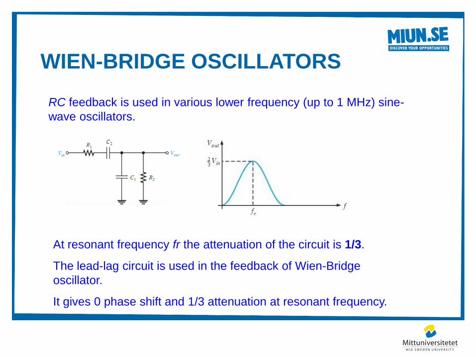
WIEN-BRIDGE OSCILLATORS
RC feedback is used in various lower frequency (up to 1 MHz) sine-
wave oscillators.
At resonant frequency fr the attenuation of the circuit is 1/3.
The lead-lag circuit is used in the feedback of Wien-Bridge
oscillator.
It gives 0 phase shift and 1/3 attenuation at resonant frequency.

WIEN-BRIDGE OSCILLATORS
The basic Wien-bridge uses the lead-lag network to select a
specific frequency that is amplified. The voltage-divider sets the
gain to make up for the attenuation of the feedback network.
The non-inverting amplifier must
have a gain of exactly 3.0 as set by
R1 and R2 to make up for the
attenuation.
If it is too little, oscillations will not
occur; if it is too much the sine
wave will be clipped.
Vout
–
+
R4
R3
R2
R1
C1
C2
Voltage-
divider
Lead-lag
network
Basic Circuit Wien Bridge Oscillator
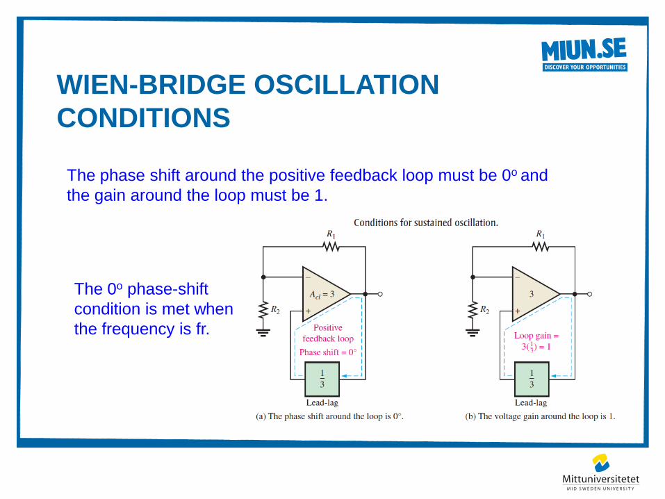
WIEN-BRIDGE OSCILLATION
CONDITIONS
The phase shift around the positive feedback loop must be 0o and
the gain around the loop must be 1.
The 0o phase-shift
condition is met when
the frequency is fr.
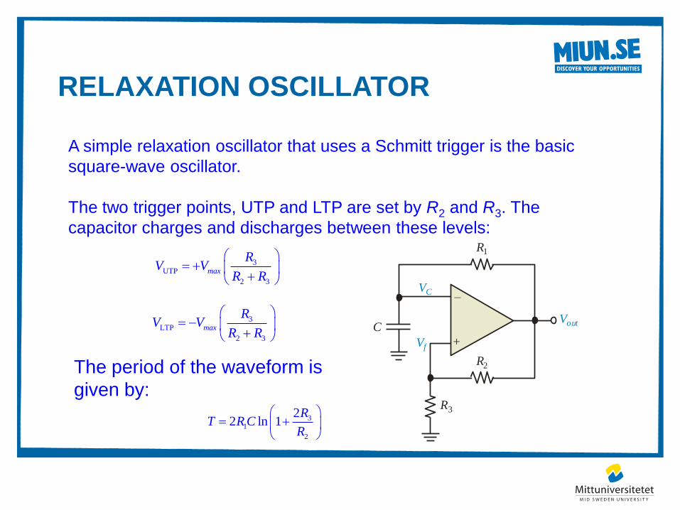
RELAXATION OSCILLATOR
A simple relaxation oscillator that uses a Schmitt trigger is the basic
square-wave oscillator.
The two trigger points, UTP and LTP are set by R2 and R3. The
capacitor charges and discharges between these levels:
The period of the waveform is
given by:
31
2
22 ln 1
RT R C
R
3UTP
2 3
max
RV V
R R
3LTP
2 3
max
RV V
R R
Vout
–
+
R2
R3
R1
Vf
VC
C

NOISE
Noise is a random fluctuation in an electrical signal.
Noise in electronic devices varies greatly, as it can be
produced by several different effects.
It is not something most designers get excited
about. In fact, they probably wish the whole
topic would go away. It can, however, be a
fascinating study by itself. A good
understanding of the underlying principles can,
in some cases, be used to reduce noise in the
design.
Noise is a fundamental parameter to be
considered in an electronic design as it typically
limits the overall performance of the system.
Noise can either be generated internally in the
op amp, from its associated passive
components, or superimposed on the circuit by
external sources.
“External” refers to noise present in the signal
being applied to the circuit or to noise
introduced into the circuit by another means,
such as conducted on a system ground or
received on one of the many antennas formed
by the traces and components in the system.

TYPES OF INTERNAL NOISE
Thermal Noise
Shot Noise
Flicker Noise
Burst Noise
Avalanche Noise
Some or all of these noises may be present in a design,
presenting a noise spectrum unique to the system.
TYPES OF INTERNAL NOISES
Thermal Noise
Shot Noise
Flicker Noise
Burst Noise
Avalanche Noise
It is not possible in most cases to separate the effects, but
knowing general causes may help the designer optimize the
design, minimizing noise in a particular bandwidth of interest.
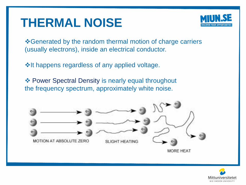
THERMAL NOISE
Generated by the random thermal motion of charge carriers
(usually electrons), inside an electrical conductor.
It happens regardless of any applied voltage.
Power Spectral Density is nearly equal throughout
the frequency spectrum, approximately white noise.
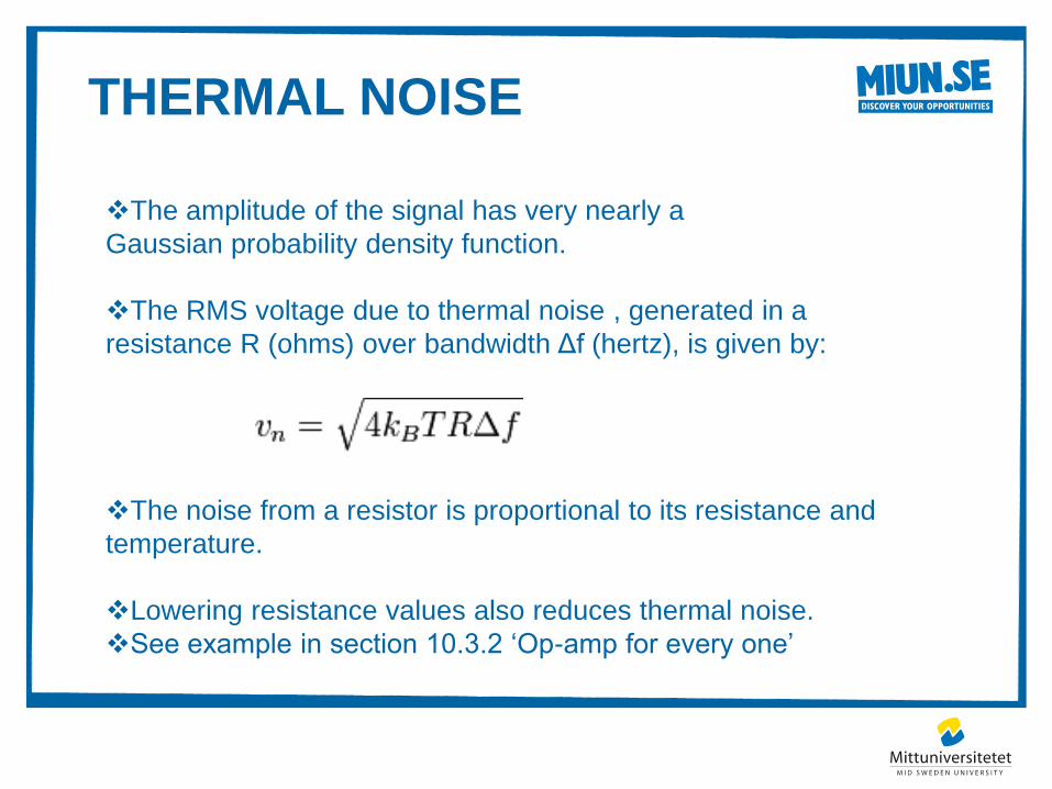
THERMAL NOISE
The amplitude of the signal has very nearly a
Gaussian probability density function.
The RMS voltage due to thermal noise , generated in a
resistance R (ohms) over bandwidth Δf (hertz), is given by:
The noise from a resistor is proportional to its resistance and
temperature.
Lowering resistance values also reduces thermal noise.
See example in section 10.3.2 ‘Op-amp for every one’
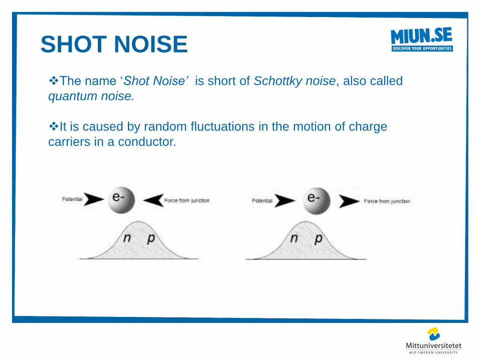
SHOT NOISE
The name ‘Shot Noise’ is short of Schottky noise, also called
quantum noise.
It is caused by random fluctuations in the motion of charge
carriers in a conductor.
SHOT NOISE
Some characteristics of shot noise:
Shot noise is always associated with current flow. It stops
when the current flow stops.
Shot noise is independent of temperature.
Shot noise is spectrally flat or has a uniform power density,
meaning that when plotted versus frequency it has a constant
value.
Shot noise is present in any conductor
FLICKER NOISE
Flicker noise is also called 1/f noise. Its origin is one of the
oldest unsolved problems in physics.
It is present in all active and many passive devices.
It may be related to imperfections in crystalline structure of
semiconductors, as better processing can reduce it.
FLICKER NOISE
Some characteristics of flicker noise:
It increases as the frequency decreases, hence the name 1/f
It is associated with a dc current in electronic devices
It has the same power content in each octave (or decade)
BURST NOISE
Burst noise consists of sudden step-like transitions between
two or more levels.
As high as several hundred microvolts.
Lasts for several milli-seconds.
Burst noise makes a popping sound at rates below 100 Hz
when played through a speaker — it sounds like popcorn
popping, hence also called popcorn noise.
Low burst noise is achieved by using clean device
processing, and therefore is beyond the control of the designer.
AVALANCHE NOISE
Avalanche noise is created when a PN junction is operated in
the reverse breakdown mode.
Under the influence of a strong reverse electric field within the
junction’s depletion region, electrons have enough kinetic
energy.
They collide with the atoms of the crystal lattice, to form
additional electron-hole pair.
These collisions are purely random and produce random
current pulses similar to shot noise, but much more intense.
AVALANCHE NOISE
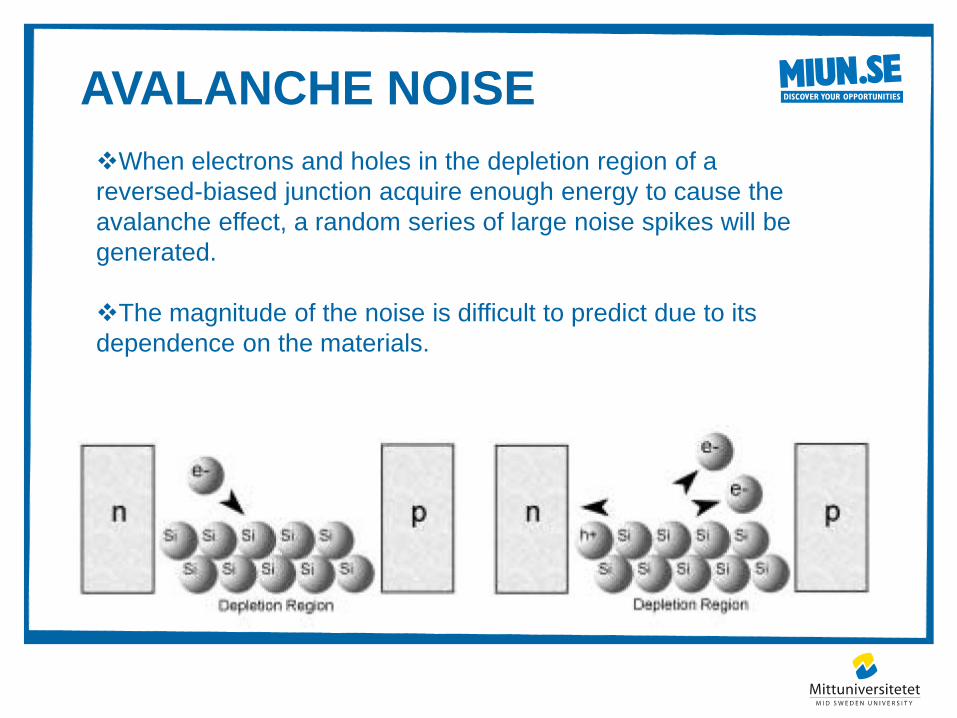
When electrons and holes in the depletion region of a
reversed-biased junction acquire enough energy to cause the
avalanche effect, a random series of large noise spikes will be
generated.
The magnitude of the noise is difficult to predict due to its
dependence on the materials.
MEASURING NOISE
RMS, PPP or PDF
NOISE FLOOR
When all input sources are turned off and the output is properly
terminated, there is a level
of noise called the noise floor that determines the smallest
signal for which the circuit is useful.
The objective for the designer is to place the signals that the
circuit processes
above the noise floor, but below the level where the signals will
clip.

SIGNAL TO NOISE RATIO
The noisiness of a signal is defined as:
In other words, it is a ratio of signal voltage to noise voltage
(hence the name signal-to-noise ratio).
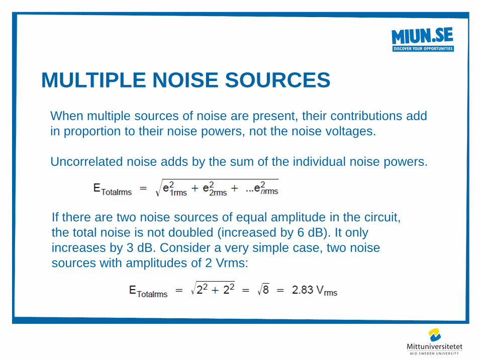
MULTIPLE NOISE SOURCES
When multiple sources of noise are present, their contributions add
in proportion to their noise powers, not the noise voltages.
Uncorrelated noise adds by the sum of the individual noise powers.
If there are two noise sources of equal amplitude in the circuit,
the total noise is not doubled (increased by 6 dB). It only
increases by 3 dB. Consider a very simple case, two noise
sources with amplitudes of 2 Vrms:

OP-AMP NOISE
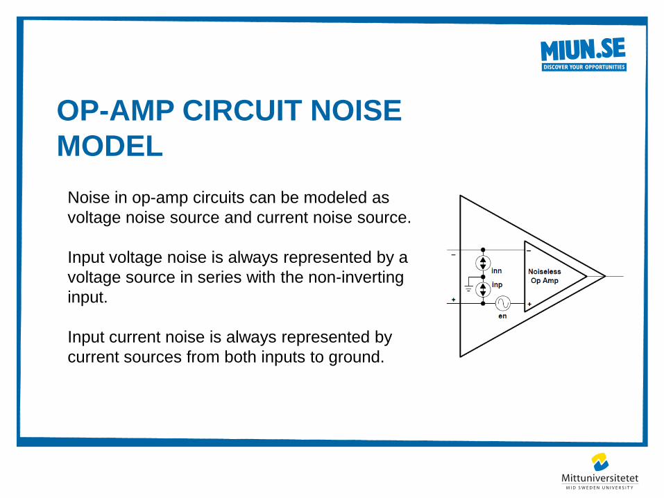
OP-AMP CIRCUIT NOISE
MODEL
Noise in op-amp circuits can be modeled as
voltage noise source and current noise source.
Input voltage noise is always represented by a
voltage source in series with the non-inverting
input.
Input current noise is always represented by
current sources from both inputs to ground.
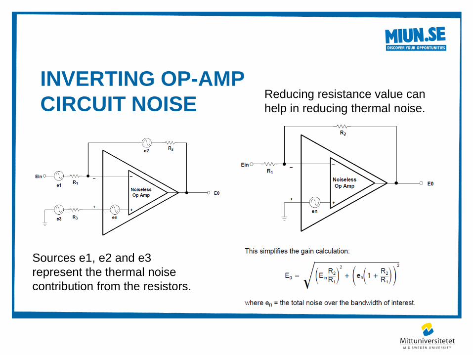
INVERTING OP-AMP
CIRCUIT NOISE
Sources e1, e2 and e3
represent the thermal noise
contribution from the resistors.
Reducing resistance value can
help in reducing thermal noise.

DIFFERENTIAL OP-AMP
CIRCUIT NOISE
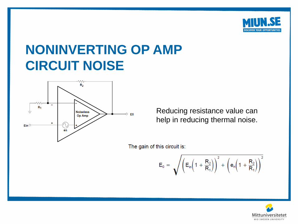
NONINVERTING OP AMP
CIRCUIT NOISE
Reducing resistance value can
help in reducing thermal noise.
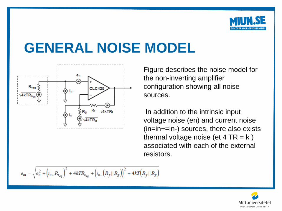
GENERAL NOISE MODEL
Figure describes the noise model for
the non-inverting amplifier
configuration showing all noise
sources.
In addition to the intrinsic input
voltage noise (en) and current noise
(in=in+=in-) sources, there also exists
thermal voltage noise (et 4 TR = k )
associated with each of the external
resistors.
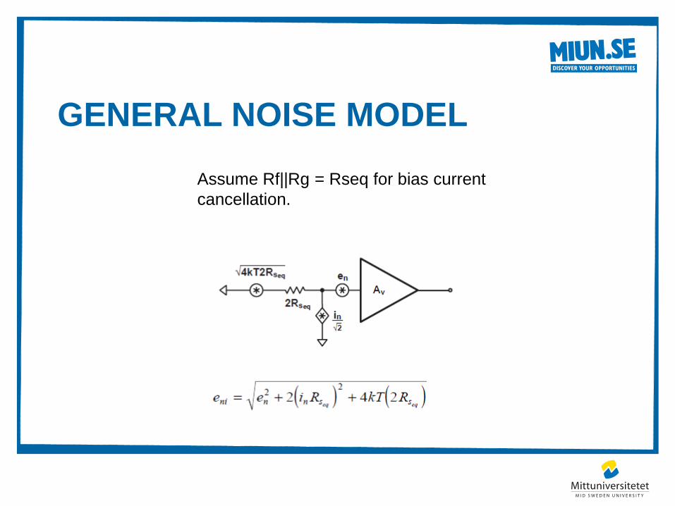
GENERAL NOISE MODEL
Assume Rf||Rg = Rseq for bias current
cancellation.
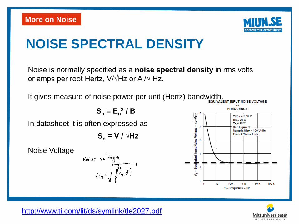
NOISE SPECTRAL DENSITY
More on Noise
Noise is normally specified as a noise spectral density in rms volts
or amps per root Hertz, V/√Hz or A /√ Hz.
It gives measure of noise power per unit (Hertz) bandwidth.
In datasheet it is often expressed as
Noise Voltage
http://www.ti.com/lit/ds/symlink/tle2027.pdf
Sn = En2 / B
Sn = V / √Hz
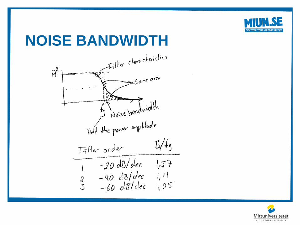
NOISE BANDWIDTH
NOISE UNIT
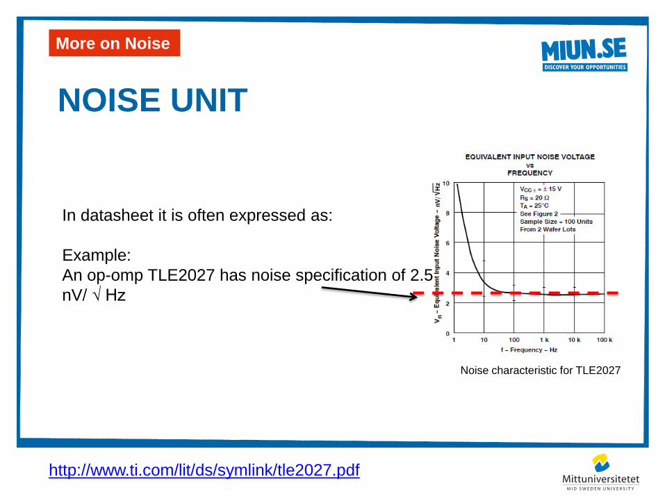
More on Noise
In datasheet it is often expressed as:
Example:
An op-omp TLE2027 has noise specification of 2.5
nV/ √ Hz
Noise characteristic for TLE2027
http://www.ti.com/lit/ds/symlink/tle2027.pdf
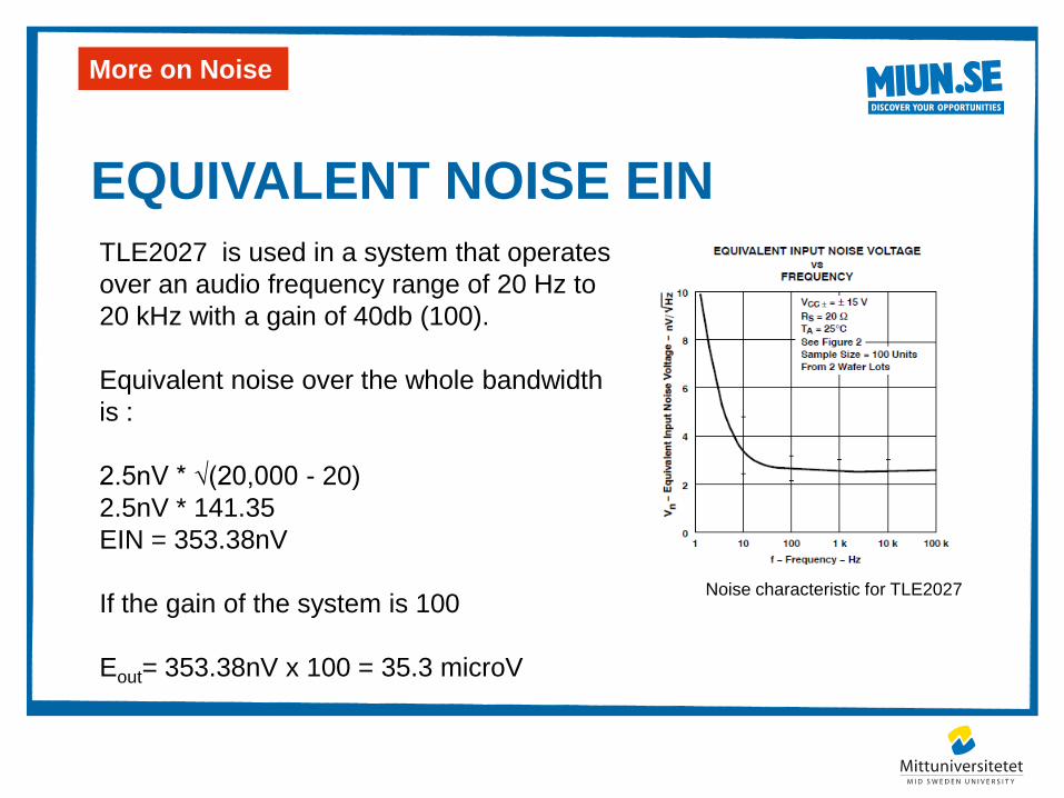
EQUIVALENT NOISE EIN
More on Noise
TLE2027 is used in a system that operates
over an audio frequency range of 20 Hz to
20 kHz with a gain of 40db (100).
Equivalent noise over the whole bandwidth
is :
2.5nV * √(20,000 - 20)
2.5nV * 141.35
EIN = 353.38nV
If the gain of the system is 100
Eout= 353.38nV x 100 = 35.3 microV
Noise characteristic for TLE2027
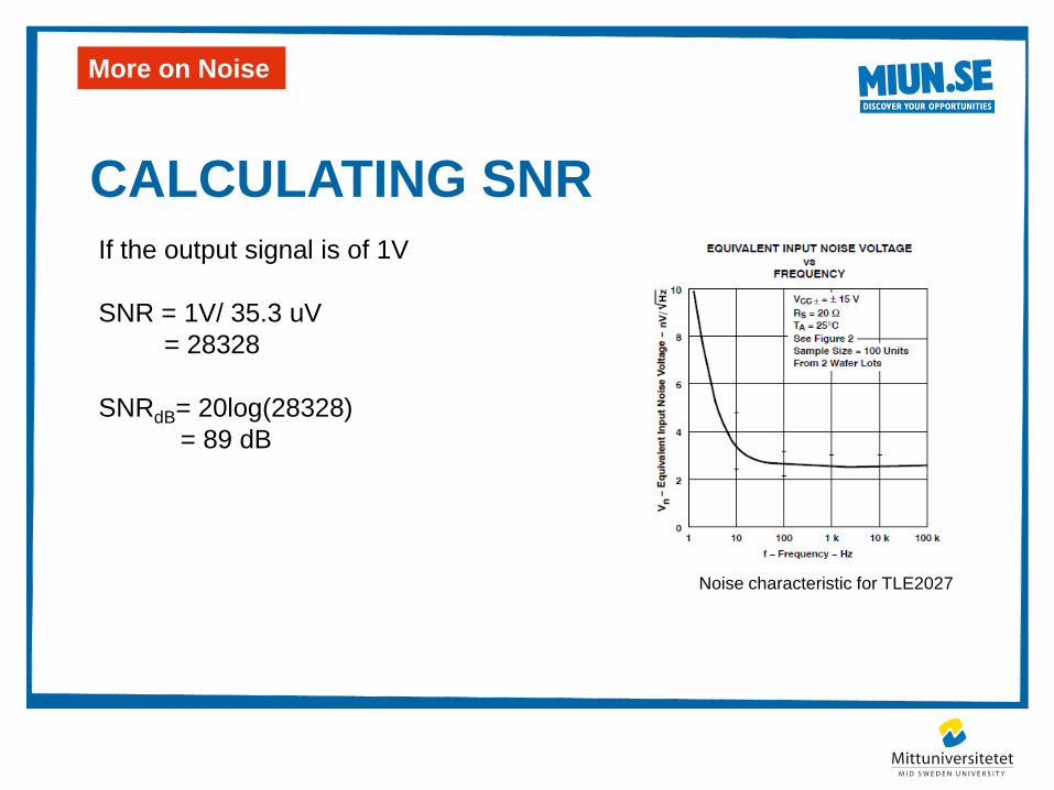
CALCULATING SNR
More on Noise
If the output signal is of 1V
SNR = 1V/ 35.3 uV
= 28328
SNRdB= 20log(28328)
= 89 dB
Noise characteristic for TLE2027


