103
Lecture Notes EECS 40 Introduction to Microelectronic Circuits Prof. C. Chang-Hasnain Spring 2007
Lecture Notes
EECS 40 Introduction to Microelectronic Circuits
Prof. C. Chang-Hasnain Spring 2007
Slide 1EE40 Fall2006
Prof. Chang-Hasnain
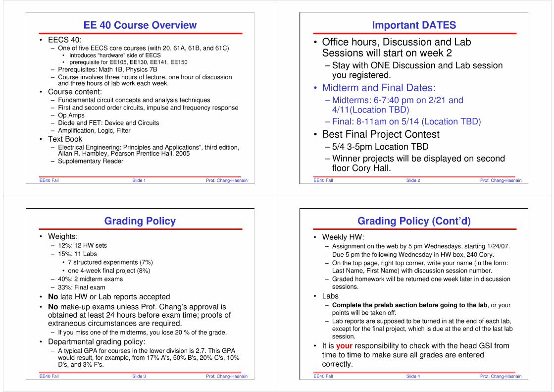
EE 40 Course Overview
• EECS 40:– One of five EECS core courses (with 20, 61A, 61B, and 61C)
• introduces “hardware” side of EECS
• prerequisite for EE105, EE130, EE141, EE150
– Prerequisites: Math 1B, Physics 7B– Course involves three hours of lecture, one hour of discussion
and three hours of lab work each week.
• Course content: – Fundamental circuit concepts and analysis techniques – First and second order circuits, impulse and frequency response– Op Amps– Diode and FET: Device and Circuits– Amplification, Logic, Filter
• Text Book– Electrical Engineering: Principles and Applications”, third edition,
Allan R. Hambley, Pearson Prentice Hall, 2005 – Supplementary Reader
Slide 2EE40 Fall2006
Prof. Chang-Hasnain
Important DATES
• Office hours, Discussion and Lab Sessions will start on week 2– Stay with ONE Discussion and Lab session
you registered.
• Midterm and Final Dates:– Midterms: 6-7:40 pm on 2/21 and
4/11(Location TBD)
– Final: 8-11am on 5/14 (Location TBD)
• Best Final Project Contest– 5/4 3-5pm Location TBD
– Winner projects will be displayed on second floor Cory Hall.
Slide 3EE40 Fall2006
Prof. Chang-Hasnain
Grading Policy
• Weights:– 12%: 12 HW sets
– 15%: 11 Labs
• 7 structured experiments (7%)
• one 4-week final project (8%)
– 40%: 2 midterm exams
– 33%: Final exam
• No late HW or Lab reports accepted
• No make-up exams unless Prof. Chang’s approval is obtained at least 24 hours before exam time; proofs of extraneous circumstances are required.– If you miss one of the midterms, you lose 20 % of the grade.
• Departmental grading policy:– A typical GPA for courses in the lower division is 2.7. This GPA
would result, for example, from 17% A's, 50% B's, 20% C's, 10% D's, and 3% F's.
Slide 4EE40 Fall2006
Prof. Chang-Hasnain
Grading Policy (Cont’d)
• Weekly HW: – Assignment on the web by 5 pm Wednesdays, starting 1/24/07.
– Due 5 pm the following Wednesday in HW box, 240 Cory.
– On the top page, right top corner, write your name (in the form:Last Name, First Name) with discussion session number.
– Graded homework will be returned one week later in discussion sessions.
• Labs– Complete the prelab section before going to the lab, or your
points will be taken off.
– Lab reports are supposed to be turned in at the end of each lab,except for the final project, which is due at the end of the last lab session.
• It is your responsibility to check with the head GSI from time to time to make sure all grades are entered
correctly.
Slide 5EE40 Fall2006
Prof. Chang-Hasnain
Classroom Rules
• Please come to class on time. There is no web-cast this semester.
• Turn off cell phones, pagers, radio, CD, DVD, etc.
• No food.
• No pets.
• Do not come in and out of classroom.
• Lectures will be recorded and webcasted.
Slide 6EE40 Fall2006
Prof. Chang-Hasnain
Chapter 1
• Outline
– Electrical quantities
• Charge, Current, Voltage, Power
– The ideal basic circuit element
– Sign conventions
– Circuit element I-V characteristics
– Construction of a circuit model
– Kirchhoff’s Current Law
– Kirchhoff’s Voltage Law
Slide 7EE40 Fall2006
Prof. Chang-Hasnain
Electric Charge
• Electrical effects are due to
– separation of charge electric force (voltage)
– charges in motion electric flow (current)
• Macroscopically, most matter is electrically
neutral most of the time.
– Exceptions: clouds in a thunderstorm, people on carpets in dry weather, plates of a charged capacitor,
etc.
• Microscopically, matter is full of electric charges
– Electric charge exists in discrete quantities, integral multiples of the electronic charge -1.6 x 10⁻¹⁹
Coulomb
Slide 8EE40 Fall2006
Prof. Chang-Hasnain
Classification of Materials
• Solids in which the outermost atomic electrons
are free to move around are metals.
– Metals typically have ~1 “free electron” per atom
– Examples:
• Solids in which all electrons are tightly bound to
atoms are insulators.
– Examples:
• Electrons in semiconductors are not tightly
bound and can be easily “promoted” to a free
state.
– Examples:
Slide 9EE40 Fall2006
Prof. Chang-Hasnain Slide 10EE40 Fall2006
Prof. Chang-Hasnain
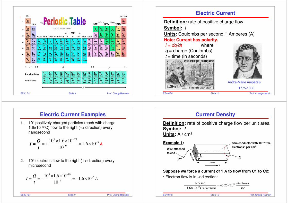
Electric Current
Definition: rate of positive charge flow
Symbol: i
Units: Coulombs per second ≡ Amperes (A)
Note: Current has polarity.
i = dq/dt where
q = charge (Coulombs)
t = time (in seconds)
1775-1836
André-Marie Ampère's
Slide 11EE40 Fall2006
Prof. Chang-Hasnain
Electric Current Examples
1. 105 positively charged particles (each with charge 1.6×10⁻¹⁹ C) flow to the right (+x direction) every
nanosecond
2. 105 electrons flow to the right (+x direction) every
microsecond
QI
t=
5 195
9
10 1.6 101.6 10
10
QI
t
−−
−
× ×= = + = × A
5 195
9
10 1.6 101.6 10
10
QI A
t
−−
−
× ×= = − = − ×
Slide 12EE40 Fall2006
Prof. Chang-Hasnain
2 cm
10 cm
1 cmC2
C1
X
Example 1:
Suppose we force a current of 1 A to flow from C1 to C2:
• Electron flow is in -x direction:
Current Density
sec 1025.6
/106.1
sec/1 18
19
electrons
electronC
C×−=
×− −
Semiconductor with 1018 “free
electrons” per cm3
Wire attached
to end
Definition: rate of positive charge flow per unit area
Symbol: J
Units: A / cm2
Slide 13EE40 Fall2006
Prof. Chang-Hasnain
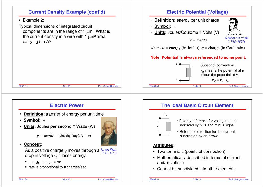
Current Density Example (cont’d)
• Example 2:
Typical dimensions of integrated circuit
components are in the range of 1 µm. What is
the current density in a wire with 1 µm² area carrying 5 mA?
Slide 14EE40 Fall2006
Prof. Chang-Hasnain
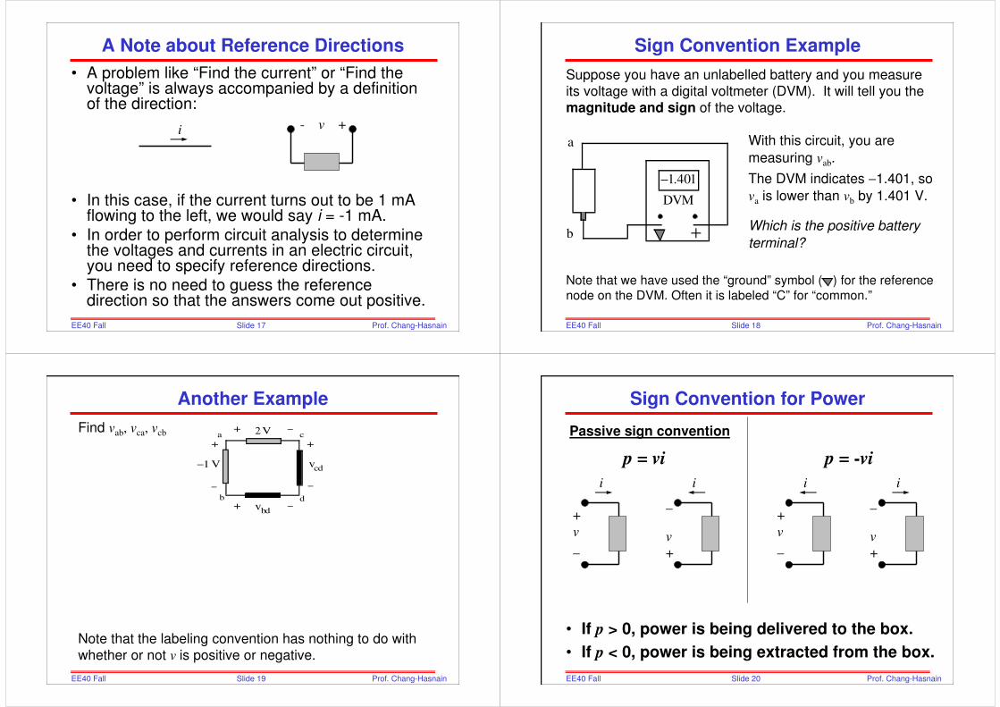
Electric Potential (Voltage)
• Definition: energy per unit charge
• Symbol: v
• Units: Joules/Coulomb ≡ Volts (V)
v = dw/dq
where w = energy (in Joules), q = charge (in Coulombs)
Note: Potential is always referenced to some point.
Subscript convention:
vab means the potential at a
minus the potential at b.
a
b vab ≡ va - vb
Alessandro Volta (1745–1827)
Slide 15EE40 Fall2006
Prof. Chang-Hasnain
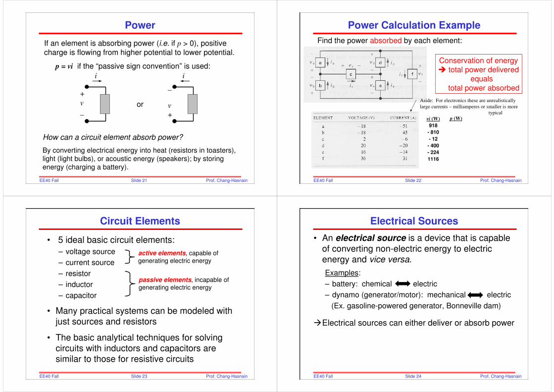
Electric Power
• Definition: transfer of energy per unit time
• Symbol: p
• Units: Joules per second ≡ Watts (W)
p = dw/dt = (dw/dq)(dq/dt) = vi
• Concept:
As a positive charge q moves through a
drop in voltage v, it loses energy
energy change = qv
rate is proportional to # charges/sec
James Watt1736 - 1819
Slide 16EE40 Fall2006
Prof. Chang-Hasnain
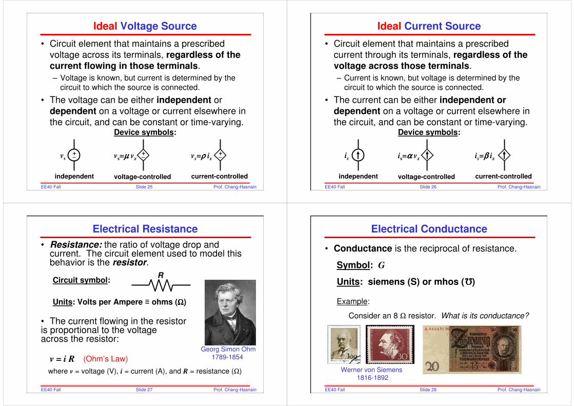
The Ideal Basic Circuit Element
Attributes:
• Two terminals (points of connection)
• Mathematically described in terms of current
and/or voltage
• Cannot be subdivided into other elements
+
v
_
i
• Polarity reference for voltage can beindicated by plus and minus signs
• Reference direction for the currentis indicated by an arrow
Slide 17EE40 Fall2006
Prof. Chang-Hasnain
- v +
A Note about Reference Directions
• A problem like “Find the current” or “Find the voltage” is always accompanied by a definition of the direction:
• In this case, if the current turns out to be 1 mA flowing to the left, we would say i = -1 mA.
• In order to perform circuit analysis to determine the voltages and currents in an electric circuit, you need to specify reference directions.
• There is no need to guess the reference direction so that the answers come out positive.
i
Slide 18EE40 Fall2006
Prof. Chang-Hasnain
Suppose you have an unlabelled battery and you measure
its voltage with a digital voltmeter (DVM). It will tell you the magnitude and sign of the voltage.
With this circuit, you are
measuring vab.
The DVM indicates −1.401, so
va is lower than vb by 1.401 V.
Which is the positive battery
terminal?
−1.401
DVM
+
a
b
Note that we have used the “ground” symbol ( ) for the reference
node on the DVM. Often it is labeled “C” for “common.”
Sign Convention Example
Slide 19EE40 Fall2006
Prof. Chang-Hasnain
Find vab, vca, vcb
Note that the labeling convention has nothing to do with whether or not v is positive or negative.
−
+
−
+
2 V
−1 V
−+
−+ vbd
vcd
a
b d
c
Another Example
Slide 20EE40 Fall2006
Prof. Chang-Hasnain
Sign Convention for Power
• If p > 0, power is being delivered to the box.
• If p < 0, power is being extracted from the box.
+
v
_
i
Passive sign convention
_
v
+
i
p = vi
+
v
_
i
_
v
+
i
p = -vi
Slide 21EE40 Fall2006
Prof. Chang-Hasnain
If an element is absorbing power (i.e. if p > 0), positive
charge is flowing from higher potential to lower potential.
p = vi if the “passive sign convention” is used:
How can a circuit element absorb power?
Power
+
v
_
i
_
v
+
i
or
By converting electrical energy into heat (resistors in toasters), light (light bulbs), or acoustic energy (speakers); by storing
energy (charging a battery).
Slide 22EE40 Fall2006
Prof. Chang-Hasnain
Find the power absorbed by each element:
Power Calculation Example
vi (W)
918
- 810
- 12
- 400
- 224
1116
p (W)
Conservation of energy
total power deliveredequals
total power absorbed
Aside: For electronics these are unrealistically
large currents – milliamperes or smaller is more
typical
Slide 23EE40 Fall2006
Prof. Chang-Hasnain
Circuit Elements
• 5 ideal basic circuit elements:
– voltage source
– current source
– resistor
– inductor
– capacitor
• Many practical systems can be modeled with
just sources and resistors
• The basic analytical techniques for solving
circuits with inductors and capacitors are
similar to those for resistive circuits
active elements, capable ofgenerating electric energy
passive elements, incapable ofgenerating electric energy
Slide 24EE40 Fall2006
Prof. Chang-Hasnain
Electrical Sources
• An electrical source is a device that is capable
of converting non-electric energy to electric
energy and vice versa.
Examples:
– battery: chemical electric
– dynamo (generator/motor): mechanical electric
(Ex. gasoline-powered generator, Bonneville dam)
Electrical sources can either deliver or absorb power
Slide 25EE40 Fall2006
Prof. Chang-Hasnain
Ideal Voltage Source
• Circuit element that maintains a prescribed
voltage across its terminals, regardless of the current flowing in those terminals.
– Voltage is known, but current is determined by the
circuit to which the source is connected.
• The voltage can be either independent or
dependent on a voltage or current elsewhere in
the circuit, and can be constant or time-varying.Device symbols:
+_vs+_vs=µ µ µ µ vx
+_vs=ρ ρ ρ ρ ix
independent voltage-controlled current-controlled
Slide 26EE40 Fall2006
Prof. Chang-Hasnain
Ideal Current Source
• Circuit element that maintains a prescribed
current through its terminals, regardless of the voltage across those terminals.
– Current is known, but voltage is determined by the
circuit to which the source is connected.
• The current can be either independent or dependent on a voltage or current elsewhere in
the circuit, and can be constant or time-varying.Device symbols:
is is=α α α α vx is=β β β β ix
independent voltage-controlled current-controlled
Slide 27EE40 Fall2006
Prof. Chang-Hasnain
Electrical Resistance
• Resistance: the ratio of voltage drop and current. The circuit element used to model this behavior is the resistor.
Circuit symbol:
Units: Volts per Ampere ≡ ohms (ΩΩΩΩ)
• The current flowing in the resistor is proportional to the voltage across the resistor:
v = i R
where v = voltage (V), i = current (A), and R = resistance (Ω)
R
(Ohm’s Law)
Georg Simon Ohm1789-1854
Slide 28EE40 Fall2006
Prof. Chang-Hasnain
Electrical Conductance
• Conductance is the reciprocal of resistance.
Symbol: G
Units: siemens (S) or mhos ( )
Example:
Consider an 8 Ω resistor. What is its conductance?
ΩΩΩΩ
Werner von Siemens 1816-1892

Slide 29EE40 Fall2006
Prof. Chang-Hasnain
Short Circuit and Open Circuit
• Short circuit
– R = 0 no voltage difference exists
– all points on the wire are at the same
potential.
– Current can flow, as determined by the circuit
• Open circuit
– R = ∞ no current flows
– Voltage difference can exist, as determined
by the circuit
Slide 30EE40 Fall2006
Prof. Chang-Hasnain
Example: Power Absorbed by a Resistor
p = vi = ( iR )i = i2R
p = vi = v ( v/R ) = v2/R
Note that p > 0 always, for a resistor a resistor
dissipates electric energy
Example:
a) Calculate the voltage vg and current ia.
b) Determine the power dissipated in the 80Ω resistor.
Slide 31EE40 Fall2006
Prof. Chang-Hasnain
More Examples
• Are these interconnections permissible?This circuit connection is permissible. This is because the current sources can sustain any voltage across; Hence this is permissible.
This circuit connection is NOT permissible. It violates the KCL.
Slide 32EE40 Fall2006
Prof. Chang-Hasnain
Summary
• Current = rate of charge flow i = dq/dt
• Voltage = energy per unit charge created by charge separation
• Power = energy per unit time
• Ideal Basic Circuit Elements– two-terminal component that cannot be sub-divided
– described mathematically in terms of its terminal voltage and current
– An ideal voltage source maintains a prescribed voltage regardless of the current in the device.
– An ideal current source maintains a prescribed current regardless of the voltage across the device.
– A resistor constrains its voltage and current to be
proportional to each other: v = iR (Ohm’s law)

Slide 33EE40 Fall2006
Prof. Chang-Hasnain
Summary (cont’d)
• Passive sign convention
– For a passive device, the reference direction
for current through the element is in the
direction of the reference voltage drop across
the element
Slide 34EE40 Fall2006
Prof. Chang-Hasnain
Current vs. Voltage (I-V) Characteristic
• Voltage sources, current sources, and resistors can be described by plotting the current (i) as a function of the voltage (v)
+
v
_
i
Passive? Active?
Slide 35EE40 Fall2006
Prof. Chang-Hasnain
I-V Characteristic of Ideal Voltage Source
1. Plot the I-V characteristic for vs > 0. For what values of i does the source absorb power? For what values of i does the source release power?
2. Repeat (1) for vs < 0.
3. What is the I-V characteristic for an ideal wire?
+_ vs
ii
+
Vab
_
v
a
b
Vs>0 i<0 release power; i>0 absorb power
i=0
Vs>0
Slide 36EE40 Fall2006
Prof. Chang-Hasnain
I-V Characteristic of Ideal Voltage Source
2. Plot the I-V characteristic for vs < 0. For what values of i does the source absorb power? For what values of i does the source release power?
+_ vs
ii
+
Vab
_
v
a
b
Vs<0 i>0 release power; i<0 absorb power
Vs<0

Slide 37EE40 Fall2006
Prof. Chang-Hasnain
I-V Characteristic of Ideal Voltage Source
3. What is the I-V characteristic for an ideal wire?
+_ vs
ii
+
Vab
_
v
a
b
Do not forget Vab=-Vba
Slide 38EE40 Fall2006
Prof. Chang-Hasnain
I-V Characteristic of Ideal Current Source
1. Plot the I-V characteristic for is > 0. For what values of v does the source absorb power? For what values of v does the source release power?
ii
+
v
_
v
is
V>0 absorb power; V<0 release power
Slide 39EE40 Fall2006
Prof. Chang-Hasnain
Short Circuit and Open Circuit
Wire (“short circuit”):
• R = 0 no voltage difference exists (all points on the wire are at the same potential)
• Current can flow, as determined by the circuit
Air (“open circuit”):
• R = ∞∞∞∞ no current flows
• Voltage difference can exist,
as determined by the circuit
Slide 40EE40 Fall2006
Prof. Chang-Hasnain
I-V Characteristic of Ideal Resistor
1. Plot the I-V characteristic for R = 1 kΩΩΩΩ. What is the slope?
ii
+
v
_
v
R
a
b
+
Vab
_R
a
b
Vab R
a
b
Slide 41EE40 Fall2006
Prof. Chang-Hasnain
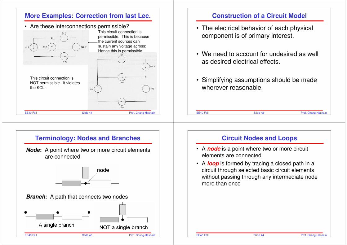
More Examples: Correction from last Lec.
• Are these interconnections permissible?This circuit connection is permissible. This is because the current sources can sustain any voltage across; Hence this is permissible.
This circuit connection is NOT permissible. It violates the KCL.
Slide 42EE40 Fall2006
Prof. Chang-Hasnain
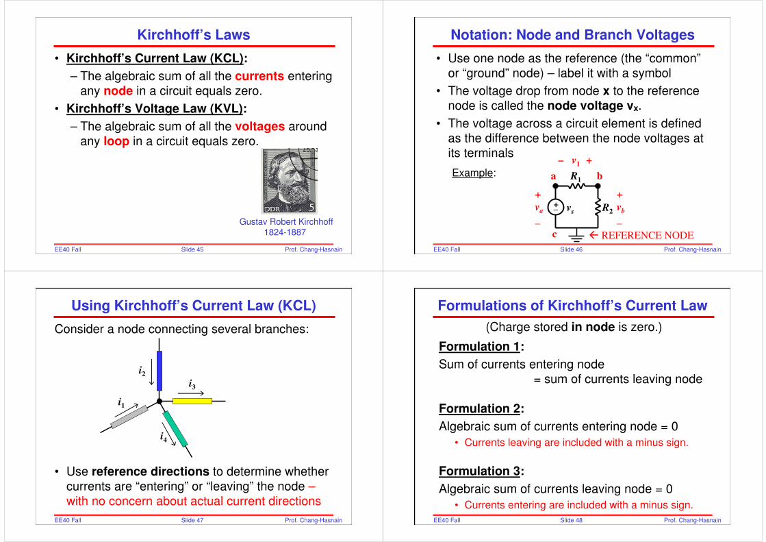
Construction of a Circuit Model
• The electrical behavior of each physical component is of primary interest.
• We need to account for undesired as well as desired electrical effects.
• Simplifying assumptions should be made wherever reasonable.
Slide 43EE40 Fall2006
Prof. Chang-Hasnain
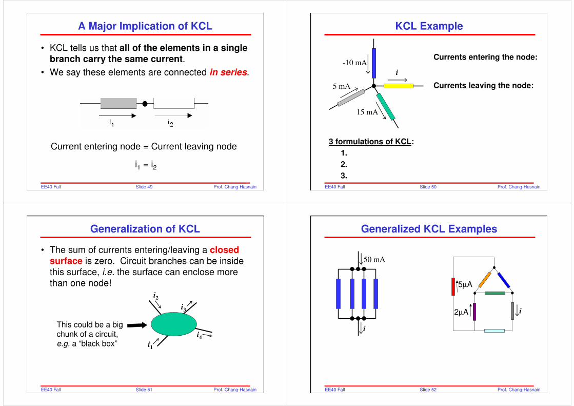
Terminology: Nodes and Branches
Node: A point where two or more circuit elements
are connected
Branch: A path that connects two nodes
Slide 44EE40 Fall2006
Prof. Chang-Hasnain
Circuit Nodes and Loops
• A node is a point where two or more circuit
elements are connected.
• A loop is formed by tracing a closed path in a
circuit through selected basic circuit elements
without passing through any intermediate node
more than once
Slide 45EE40 Fall2006
Prof. Chang-Hasnain
Kirchhoff’s Laws
• Kirchhoff’s Current Law (KCL):
– The algebraic sum of all the currents entering
any node in a circuit equals zero.
• Kirchhoff’s Voltage Law (KVL):
– The algebraic sum of all the voltages around
any loop in a circuit equals zero.
Gustav Robert Kirchhoff1824-1887
Slide 46EE40 Fall2006
Prof. Chang-Hasnain
Notation: Node and Branch Voltages
• Use one node as the reference (the “common”
or “ground” node) – label it with a symbol
• The voltage drop from node x to the reference
node is called the node voltage vx.
• The voltage across a circuit element is defined
as the difference between the node voltages at
its terminals
Example:
+_ vs
+
va
_
+
vb
_
a b
c
R1
R2
– v1 +
REFERENCE NODE
Slide 47EE40 Fall2006
Prof. Chang-Hasnain
• Use reference directions to determine whether
currents are “entering” or “leaving” the node –
with no concern about actual current directions
Using Kirchhoff’s Current Law (KCL)
i1
i4
i3
i2
Consider a node connecting several branches:
Slide 48EE40 Fall2006
Prof. Chang-Hasnain
Formulations of Kirchhoff’s Current Law
Formulation 1:
Sum of currents entering node
= sum of currents leaving node
Formulation 2:
Algebraic sum of currents entering node = 0
• Currents leaving are included with a minus sign.
Formulation 3:
Algebraic sum of currents leaving node = 0
• Currents entering are included with a minus sign.
(Charge stored in node is zero.)
Slide 49EE40 Fall2006
Prof. Chang-Hasnain
A Major Implication of KCL
• KCL tells us that all of the elements in a single branch carry the same current.
• We say these elements are connected in series.
Current entering node = Current leaving node
i1 = i2
Slide 50EE40 Fall2006
Prof. Chang-Hasnain
KCL Example
5 mA
15 mA
i
-10 mA
3 formulations of KCL:
1.
2.
3.
Currents entering the node:
Currents leaving the node:
Slide 51EE40 Fall2006
Prof. Chang-Hasnain
Generalization of KCL
• The sum of currents entering/leaving a closed surface is zero. Circuit branches can be inside
this surface, i.e. the surface can enclose more
than one node!
This could be a big chunk of a circuit,
e.g. a “black box” i1
i2
i3
i4
Slide 52EE40 Fall2006
Prof. Chang-Hasnain
Generalized KCL Examples
5µA
2µA i
50 mA
i
Slide 53EE40 Fall2006
Prof. Chang-Hasnain
• Use reference polarities to determine whether a
voltage is dropped
• No concern about actual voltage polarities
Using Kirchhoff’s Voltage Law (KVL)
Consider a branch which forms part of a loop:
+
v1
_
loop
Moving from + to -We add V1
–
v2
+
loop
Moving from - to +We subtract V1
Slide 54EE40 Fall2006
Prof. Chang-Hasnain
Formulations of Kirchhoff’s Voltage Law
Formulation 1:
Sum of voltage drops around loop
= sum of voltage rises around loop
Formulation 2:
Algebraic sum of voltage drops around loop = 0
• Voltage rises are included with a minus sign.
Formulation 3:
Algebraic sum of voltage rises around loop = 0
• Voltage drops are included with a minus sign.
(Conservation of energy)
(Handy trick: Look at the first sign you encounter on each element when tracing the loop.)
Slide 55EE40 Fall2006
Prof. Chang-Hasnain
A Major Implication of KVL
• KVL tells us that any set of elements which are connected at both ends carry the same voltage.
• We say these elements are connected in parallel.
Applying KVL in the clockwise direction,
starting at the top:vb – va = 0 vb = va
+
va
_
+
vb
_
Slide 56EE40 Fall2006
Prof. Chang-Hasnain
Path 1:
Path 2:
Path 3:
vcva
+
−
+
−
3
21
+ −
vb
v3v2
+ −
+
-
Three closed paths:
a b c
KVL Example

Slide 57EE40 Fall2006
Prof. Chang-Hasnain
• No time-varying magnetic flux through the loop
Otherwise, there would be an induced voltage (Faraday’s Law)
Avoid these loops!
How do we deal with antennas (EECS 117A)?
Include a voltage source as the circuit representation of the induced voltage or “noise”.
(Use a lumped model rather than a distributed (wave) model.)
• Note: Antennas are designed to “pick up”electromagnetic waves; “regular circuits”
often do so undesirably.)t(B
)t(v+ −
An Underlying Assumption of KVL
Slide 58EE40 Fall2006
Prof. Chang-Hasnain
I-V Characteristic of Elements
Find the I-V characteristic.
+_ vs
i
i+
Vab
_
v
a
b
R
Slide 59EE40 Fall2006
Prof. Chang-Hasnain
Summary
• An electrical system can be modeled by an electric circuit(combination of paths, each containing 1 or more circuit elements) – Lumped model
• The Current versus voltage characteristics (I-V plot) is a universal means of describing a circuit element.
• Kirchhoff’s current law (KCL) states that the algebraic sum of all currents at any node in a circuit equals zero.
– Comes from conservation of charge
• Kirchhoff’s voltage law (KVL) states that the algebraic sum of all voltages around any closed path in a circuit equals zero.
– Comes from conservation of potential energy
Slide 60EE40 Fall2006
Prof. Chang-Hasnain
Chapter 2
• Outline
– Resistors in Series – Voltage Divider
– Conductances in Parallel – Current Divider
– Node-Voltage Analysis
– Mesh-Current Analysis
– Superposition
– Thévenin equivalent circuits
– Norton equivalent circuits
– Maximum Power Transfer
Slide 61EE40 Fall2006
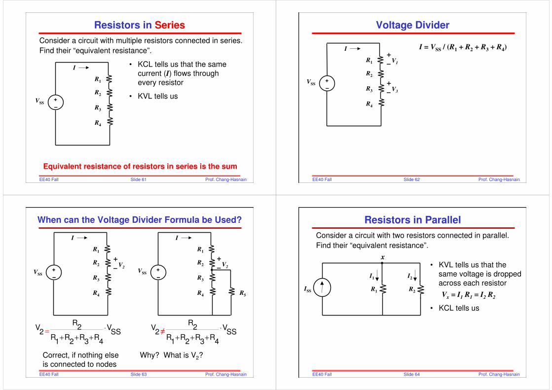
Prof. Chang-Hasnain
Consider a circuit with multiple resistors connected in series.
Find their “equivalent resistance”.
• KCL tells us that the same current (I) flows through
every resistor
• KVL tells us
Equivalent resistance of resistors in series is the sum
R2
R1
VSS
I
R3
R4
−−−−
+
Resistors in Series
Slide 62EE40 Fall2006
Prof. Chang-Hasnain
I = VSS / (R1 + R2 + R3 + R4)
Voltage Divider
+
– V1
+
– V3
R2
R1
VSS
I
R3
R4
−−−−
+
Slide 63EE40 Fall2006
Prof. Chang-Hasnain
SS
4321
22
V
RRRR
RV ⋅
+++=
Correct, if nothing else
is connected to nodes
Why? What is V2?
SS
4321
22
V
RRRR
RV ⋅
+++≠
When can the Voltage Divider Formula be Used?
+
– V2R2
R1
VSS
I
R3
R4
−−−−
+R2
R1
VSS
I
R3
R4
−−−−
+
R5
+
–V2
Slide 64EE40 Fall2006
Prof. Chang-Hasnain
• KVL tells us that the
same voltage is droppedacross each resistor
Vx = I1 R1 = I2 R2
• KCL tells us
R2R1ISS
I2I1
x
Resistors in Parallel
Consider a circuit with two resistors connected in parallel.
Find their “equivalent resistance”.
Slide 65EE40 Fall2006
Prof. Chang-Hasnain
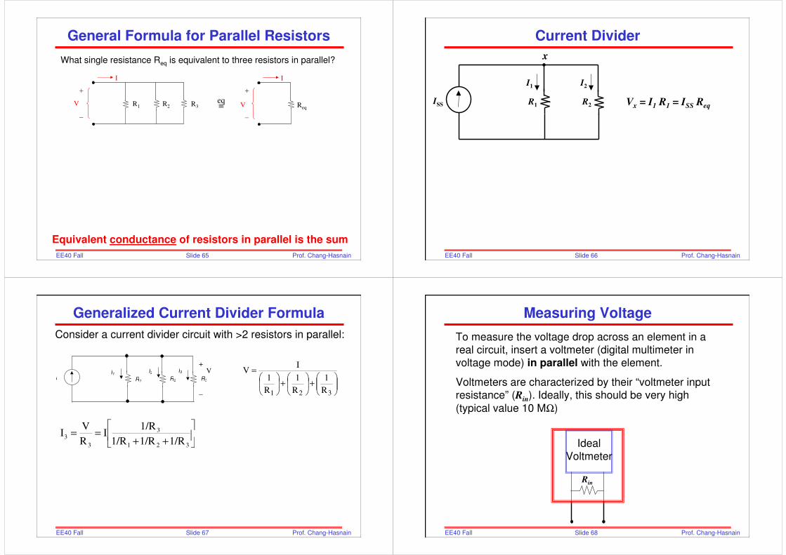
What single resistance Req is equivalent to three resistors in parallel?
+
−
V
I
V
+
−
I
R3R2R1 Req
eq≡
General Formula for Parallel Resistors
Equivalent conductance of resistors in parallel is the sum
Slide 66EE40 Fall2006
Prof. Chang-Hasnain
Vx = I1 R1 = ISS Req
Current Divider
R2R1ISS
I2I1
x
Slide 67EE40 Fall2006
Prof. Chang-Hasnain
R2R1 I
I2I1 I3
R3
+
−
V
+
+
=
321 R
1
R
1
R
1
IV
++==
321
3
3
31/R1/R1/R
1/RI
R
VI
Generalized Current Divider Formula
Consider a current divider circuit with >2 resistors in parallel:
Slide 68EE40 Fall2006
Prof. Chang-Hasnain
To measure the voltage drop across an element in a real circuit, insert a voltmeter (digital multimeter in
voltage mode) in parallel with the element.
Voltmeters are characterized by their “voltmeter input resistance” (Rin). Ideally, this should be very high
(typical value 10 MΩ)
Ideal
Voltmeter
Rin
Measuring Voltage
Slide 69EE40 Fall2006
Prof. Chang-Hasnain
+=
21
2SS2
RR
RVV
+=′
1in2
in2SS2
RR||R
R||RVV
Example: V1VK900R ,K100R ,V10V 212SS =⇒===
VSS
R1
R2
210 , ?inR M V ′= =
Effect of Voltmeter
undisturbed circuit circuit with voltmeter inserted
_++
–
V2VSS
R1
R2 Rin
_++
–
V2′
Compare to R2
Slide 70EE40 Fall2006
Prof. Chang-Hasnain
To measure the current flowing through an element in a
real circuit, insert an ammeter (digital multimeter in current mode) in series with the element.
Ammeters are characterized by their “ammeter input resistance” (Rin). Ideally, this should be very low
(typical value 1Ω).
Ideal Ammeter
Rin
Measuring Current
Slide 71EE40 Fall2006
Prof. Chang-Hasnain
Rin
V1
Imeas
R1
R2
ammeter
circuit with ammeter inserted
_+V1
I
R1
R2
undisturbed circuit
Example: V1 = 1 V, R1= R2 = 500 Ω, Rin = 1Ω
21
1
RR
VI
+=
in21
1meas
RRR
VI
++=
11 , ?
500 500meas
VI mA I= = =
Ω + Ω
Effect of Ammeter
Measurement error due to non-zero input resistance:
_+
Compare to
R2 + R2
Slide 72EE40 Fall2006
Prof. Chang-Hasnain
Simplify a circuit before applying KCL and/or KVL:
−
+7 V
Using Equivalent Resistances
R1 = R2 = 3 kΩR3 = 6 kΩ
R4 = R5 = 5 kΩR6 = 10 kΩ
I
R1
R2
R4
R5
R3
R6
Example: Find I
Slide 73EE40 Fall2006
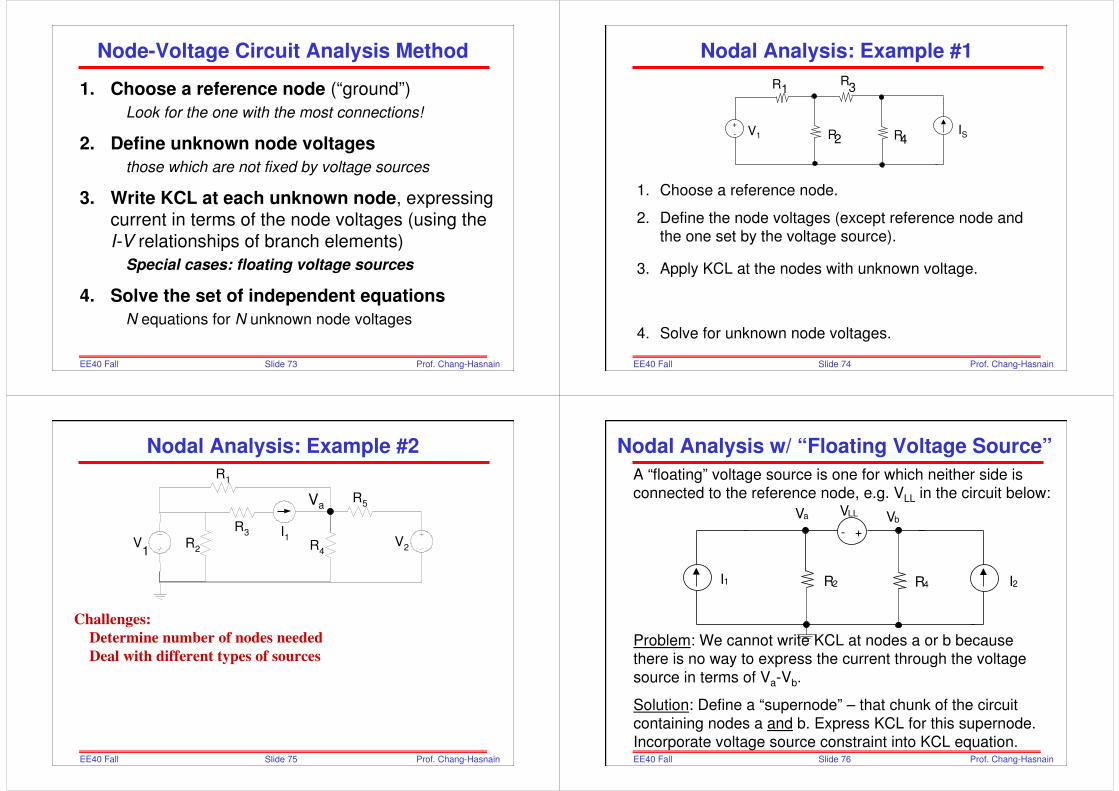
Prof. Chang-Hasnain
1. Choose a reference node (“ground”)
Look for the one with the most connections!
2. Define unknown node voltages
those which are not fixed by voltage sources
3. Write KCL at each unknown node, expressing
current in terms of the node voltages (using the
I-V relationships of branch elements)
Special cases: floating voltage sources
4. Solve the set of independent equations
N equations for N unknown node voltages
Node-Voltage Circuit Analysis Method
Slide 74EE40 Fall2006
Prof. Chang-Hasnain
1. Choose a reference node.
2. Define the node voltages (except reference node and the one set by the voltage source).
3. Apply KCL at the nodes with unknown voltage.
4. Solve for unknown node voltages.
R4V1 R2
+
- IS
R3R1
Nodal Analysis: Example #1
Slide 75EE40 Fall2006
Prof. Chang-Hasnain
V2V1
R2
R1
R4
R5
R3 I1
Va
Nodal Analysis: Example #2
Challenges:
Determine number of nodes needed
Deal with different types of sources
Slide 76EE40 Fall2006
Prof. Chang-Hasnain
A “floating” voltage source is one for which neither side is connected to the reference node, e.g. VLL in the circuit below:
Problem: We cannot write KCL at nodes a or b because there is no way to express the current through the voltage
source in terms of Va-Vb.
Solution: Define a “supernode” – that chunk of the circuit
containing nodes a and b. Express KCL for this supernode.
Incorporate voltage source constraint into KCL equation.
R4R2 I2
Va Vb
+-
VLL
I1
Nodal Analysis w/ “Floating Voltage Source”
Slide 77EE40 Fall2006
Prof. Chang-Hasnain
supernode
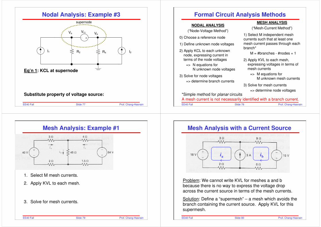
Eq’n 1: KCL at supernode
Substitute property of voltage source:
R4R2 I2
Va Vb
+-
VLL
I1
Nodal Analysis: Example #3
Slide 78EE40 Fall2006
Prof. Chang-Hasnain
NODAL ANALYSIS
(“Node-Voltage Method”)
0) Choose a reference node
1) Define unknown node voltages
2) Apply KCL to each unknown node, expressing current in terms of the node voltages
=> N equations forN unknown node voltages
3) Solve for node voltages
=> determine branch currents
MESH ANALYSIS
(“Mesh-Current Method”)
1) Select M independent mesh currents such that at least one mesh current passes through each branch*
M = #branches - #nodes + 1
2) Apply KVL to each mesh, expressing voltages in terms of mesh currents
=> M equations forM unknown mesh currents
3) Solve for mesh currents
=> determine node voltages
Formal Circuit Analysis Methods
*Simple method for planar circuits
A mesh current is not necessarily identified with a branch current.
Slide 79EE40 Fall2006
Prof. Chang-Hasnain
1. Select M mesh currents.
2. Apply KVL to each mesh.
3. Solve for mesh currents.
Mesh Analysis: Example #1
Slide 80EE40 Fall2006
Prof. Chang-Hasnain
Problem: We cannot write KVL for meshes a and b because there is no way to express the voltage drop
across the current source in terms of the mesh currents.
Solution: Define a “supermesh” – a mesh which avoids the
branch containing the current source. Apply KVL for this
supermesh.
Mesh Analysis with a Current Source
ia ib

Slide 81EE40 Fall2006
Prof. Chang-Hasnain
Eq’n 1: KVL for supermesh
Eq’n 2: Constraint due to current source:
Mesh Analysis: Example #2
ia ib
Slide 82EE40 Fall2006
Prof. Chang-Hasnain
Mesh Analysis with Dependent Sources
• Exactly analogous to Node Analysis
• Dependent Voltage Source: (1) Formulate and write KVL mesh eqns. (2) Include and express dependency constraint in terms of mesh currents
• Dependent Current Source: (1) Use supermesh. (2) Include and express dependency constraint in terms of mesh currents
Slide 83EE40 Fall2006
Prof. Chang-Hasnain
Find i2, i1 and io
Circuit w/ Dependent Source Example
Slide 84EE40 Fall2006
Prof. Chang-Hasnain
Superposition
A linear circuit is one constructed only of linear
elements (linear resistors, and linear capacitors and
inductors, linear dependent sources) and
independent sources. Linear
means I-V charcteristic of elements/sources are
straight lines when plotted
Principle of Superposition:
• In any linear circuit containing multiple
independent sources, the current or voltage at
any point in the network may be calculated as
the algebraic sum of the individual contributions
of each source acting alone.

Slide 85EE40 Fall2006
Prof. Chang-Hasnain
• Voltage sources in series can be replaced by an
equivalent voltage source:
• Current sources in parallel can be replaced by
an equivalent current source:
Source Combinations
i1 i2 ≡ i1+i2
–+
–+
v1
v2
≡
–+
v1+v2
Slide 86EE40 Fall2006
Prof. Chang-Hasnain
Superposition
Procedure:1. Determine contribution due to one independent source
• Set all other sources to 0: Replace independent voltagesource by short circuit, independent current source by opencircuit
2. Repeat for each independent source
3. Sum individual contributions to obtain desired voltage
or current
Slide 87EE40 Fall2006
Prof. Chang-Hasnain
Open Circuit and Short Circuit
• Open circuit i=0 ; Cut off the branch
• Short circuit v=0 ; replace the element by wire
• Turn off an independent voltage source means
– V=0
– Replace by wire
– Short circuit
• Turn off an independent current source means
– i=0
– Cut off the branch
– open circuit
Slide 88EE40 Fall2006
Prof. Chang-Hasnain
Superposition Example
• Find Vo
–+
24 V
2 Ω
4 Ω4 A
4 V
+ –+
Vo
–
Slide 89EE40 Fall2006
Prof. Chang-Hasnain
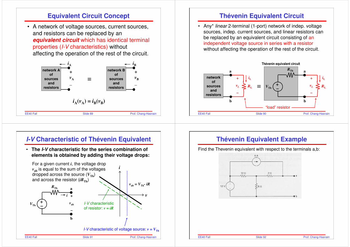
Equivalent Circuit Concept
• A network of voltage sources, current sources,
and resistors can be replaced by an
equivalent circuit which has identical terminal
properties (I-V characteristics) without
affecting the operation of the rest of the circuit.
+
vA
_
network Aof
sourcesand
resistors
iA
≡
+
vB
_
network Bof
sourcesand
resistors
iB
iA(vA) = iB(vB)
Slide 90EE40 Fall2006
Prof. Chang-Hasnain
Thévenin Equivalent Circuit
• Any* linear 2-terminal (1-port) network of indep. voltage sources, indep. current sources, and linear resistors can
be replaced by an equivalent circuit consisting of an
independent voltage source in series with a resistorwithout affecting the operation of the rest of the circuit.
networkof
sourcesand
resistors
≡ –+
VTh
RTh
RL
iL+
vL
–
a
b
RL
iL+
vL
–
a
b
Thévenin equivalent circuit
“load” resistor
Slide 91EE40 Fall2006
Prof. Chang-Hasnain
I-V Characteristic of Thévenin Equivalent
• The I-V characteristic for the series combination of elements is obtained by adding their voltage drops:
–+
VTh
RTh a
b
i
i
+
vab
–
vab = VTh- iR
I-V characteristic of resistor: v = iR
I-V characteristic of voltage source: v = VTh
For a given current i, the voltage drop
vab is equal to the sum of the voltages
dropped across the source (VTh)
and across the resistor (iRTh)
v
Slide 92EE40 Fall2006
Prof. Chang-Hasnain
Thévenin Equivalent Example
Find the Thevenin equivalent with respect to the terminals a,b:
Slide 93EE40 Fall2006
Prof. Chang-Hasnain
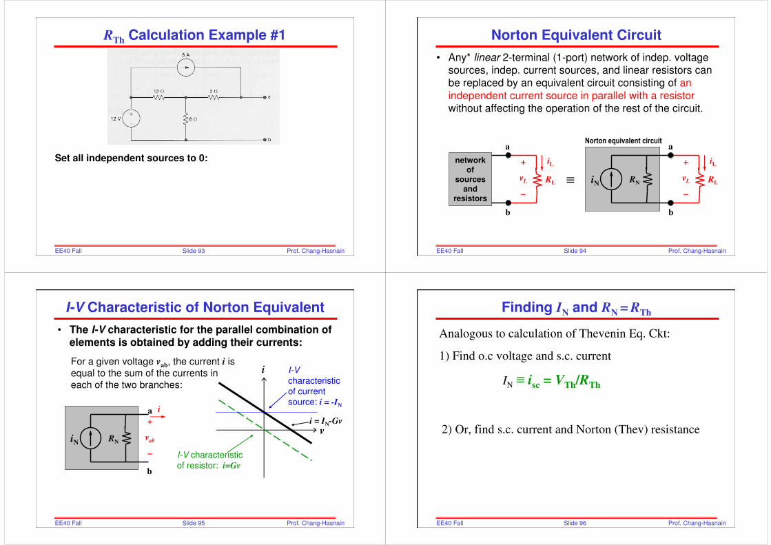
RTh Calculation Example #1
Set all independent sources to 0:
Slide 94EE40 Fall2006
Prof. Chang-Hasnain
Norton equivalent circuit
Norton Equivalent Circuit
• Any* linear 2-terminal (1-port) network of indep. voltage sources, indep. current sources, and linear resistors can
be replaced by an equivalent circuit consisting of an
independent current source in parallel with a resistorwithout affecting the operation of the rest of the circuit.
networkof
sourcesand
resistors
≡RL
iL+
vL
–
a
b
a
RL
iL+
vL
–
iN
b
RN
Slide 95EE40 Fall2006
Prof. Chang-Hasnain
I-V Characteristic of Norton Equivalent
• The I-V characteristic for the parallel combination of elements is obtained by adding their currents:
i
i = IN-Gv
I-V characteristic of resistor: i=Gv
I-Vcharacteristic of current source: i = -IN
For a given voltage vab, the current i is
equal to the sum of the currents in
each of the two branches:
v
i
+
vab
–
iN
b
RN
a
Slide 96EE40 Fall2006
Prof. Chang-Hasnain
Finding IN and RN = RTh
IN ≡ isc = VTh/RTh
Analogous to calculation of Thevenin Eq. Ckt:
1) Find o.c voltage and s.c. current
2) Or, find s.c. current and Norton (Thev) resistance
Slide 97EE40 Fall2006
Prof. Chang-Hasnain
Finding IN and RN
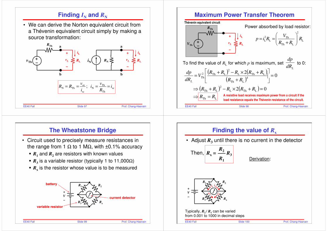
• We can derive the Norton equivalent circuit from
a Thévenin equivalent circuit simply by making a
source transformation:
RLRN
iL
iN
+
vL
–
a
b
–+
RL
iL+
vL
–
vTh
RTh
sc
Th
ThN
sc
ocThN ; i
R
vi
i
vRR ====
a
b
Slide 98EE40 Fall2006
Prof. Chang-Hasnain
Maximum Power Transfer Theorem
A resistive load receives maximum power from a circuit if the
load resistance equals the Thévenin resistance of the circuit.
L
2
LTh
ThL
2
L RRR
VRip
+==
–+
VTh
RTh
RL
iL+
vL
–
Thévenin equivalent circuit
( ) ( )( )
( ) ( )
LTh
LThL
2
LTh
4
LTh
LThL
2
LTh2
Th
02
02
RR
RRRRR
RR
RRRRRV
dR
dp
L
=⇒
=+×−+⇒
=
+
+×−+=
To find the value of RL for which p is maximum, set to 0:
Power absorbed by load resistor:
LdR
dp
Slide 99EE40 Fall2006
Prof. Chang-Hasnain
The Wheatstone Bridge
• Circuit used to precisely measure resistances in
the range from 1 Ω to 1 MΩ, with ±0.1% accuracy
R1 and R2 are resistors with known values
R3 is a variable resistor (typically 1 to 11,000Ω)
Rx is the resistor whose value is to be measured
+
V
–
R1 R2
R3 Rx
current detector
battery
variable resistor
Slide 100EE40 Fall2006
Prof. Chang-Hasnain
Finding the value of Rx
• Adjust R3 until there is no current in the detector
Then,
+
V
–
R1 R2
R3 Rx
Rx = R3
R2
R1 Derivation:
i1 i2
ixi3
Typically, R2 / R1 can be varied
from 0.001 to 1000 in decimal steps

Slide 101EE40 Fall2006
Prof. Chang-Hasnain
Finding the value of Rx
• Adjust R3 until there is no current in the detector
Then,
+
V
–
R1 R2
R3 Rx
Rx = R3
R2
R1 Derivation:
i1 = i3 and i2 = ix
i3R3 = ixRx and i1R1 = i2R2
i1R3 = i2Rx
KCL =>
KVL =>
R3
R1
Rx
R2
=
i1 i2
ixi3
Typically, R2 / R1 can be varied
from 0.001 to 1000 in decimal steps
Slide 102EE40 Fall2006
Prof. Chang-Hasnain
Some circuits must be analyzed (not amenable to simple inspection)
-
+ R2
R1
V
I
R4
R3
R5
Special cases:
R3 = 0 OR R3 = ∞
R1
−
+
R4R5
R2
V R3
Identifying Series and Parallel Combinations
Slide 103EE40 Fall2006
Prof. Chang-Hasnain
Y-Delta Conversion
• These two resistive circuits are equivalent for
voltages and currents external to the Y and ∆circuits. Internally, the voltages and currents
are different.
R1 R2
R3
c
ba
R1 R2
R3
c
b
R1 R2
R3
c
baRc
a b
c
Rb Ra
Rc
a b
c
Rb Ra
a b
c
Rb Ra
R1 =RbRc
Ra + Rb + Rc
R2 =RaRc
Ra + Rb + Rc
R3 =RaRb
Ra + Rb + Rc
Brain Teaser Category: Important for motors and electrical utilities.
Slide 104EE40 Fall2006
Prof. Chang-Hasnain
Delta-to-Wye (Pi-to-Tee) Equivalent Circuits
• In order for the Delta interconnection to be equivalent to the Wye interconnection, the resistance between
corresponding terminal pairs must be the same
Rab = = R1 + R2
Rc (Ra + Rb)
Ra + Rb + Rc
Rbc = = R2 + R3
Ra (Rb + Rc)
Ra + Rb + Rc
Rca = = R1 + R3
Rb (Ra + Rc)
Ra + Rb + Rc
Rc
a b
c
Rb Ra
R1 R2
R3
c
ba

Slide 105EE40 Fall2006
Prof. Chang-Hasnain
∆∆∆∆-Y and Y-∆∆∆∆ Conversion Formulas
R1 R2
R3
c
ba
R1 R2
R3
c
b
R1 R2
R3
c
ba
R1 =RbRc
Ra + Rb + Rc
R2 =RaRc
Ra + Rb + Rc
R3 =RaRb
Ra + Rb + Rc
Delta-to-Wye conversion Wye-to-Delta conversion
Ra =R1R2 + R2R3 + R3R1
R1
Rb =R1R2 + R2R3 + R3R1
R2
Rc =R1R2 + R2R3 + R3R1
R3
Rc
a b
c
Rb Ra
Rc
a b
c
Rb Ra
a b
c
Rb Ra
Slide 106EE40 Fall2006
Prof. Chang-Hasnain
Circuit Simplification Example
Find the equivalent resistance Rab:2ΩΩΩΩ
a
b
18ΩΩΩΩ6ΩΩΩΩ
12ΩΩΩΩ
4ΩΩΩΩ9ΩΩΩΩ
≡
2ΩΩΩΩ
a
b4ΩΩΩΩ9ΩΩΩΩ
Slide 107EE40 Fall2006
Prof. Chang-Hasnain
Dependent Sources
• Node-Voltage Method – Dependent current source:
• treat as independent current source in organizing node eqns
• substitute constraining dependency in terms of defined node voltages.
– Dependent voltage source:
• treat as independent voltage source in organizing node eqns
• Substitute constraining dependency in terms of defined node voltages.
• Mesh Analysis– Dependent Voltage Source:
• Formulate and write KVL mesh eqns.
• Include and express dependency constraint in terms of mesh currents
– Dependent Current Source:
• Use supermesh.
• Include and express dependency constraint in terms of mesh currents
Slide 108EE40 Fall2006
Prof. Chang-Hasnain
Comments on Dependent Sources
A dependent source establishes a voltage or current whose value depends on the value of a voltage or current at a specified location in the circuit.
(device model, used to model behavior of transistors & amplifiers)
To specify a dependent source, we must identify:1. the controlling voltage or current (must be calculated, in general)
2. the relationship between the controlling voltage or current and the supplied voltage or current
3. the reference direction for the supplied voltage or current
The relationship between the dependent sourceand its reference cannot be broken!
– Dependent sources cannot be turned off for various purposes (e.g. to find the Thévenin resistance, or in analysis using Superposition).
Slide 109EE40 Fall2006
Prof. Chang-Hasnain
Node-Voltage Method and Dependent Sources
• If a circuit contains dependent sources, what to do?
Example:
–+
–+
80 V
5i∆
20 Ω
10 Ω
20 Ω2.4 A
i∆
Slide 110EE40 Fall2006
Prof. Chang-Hasnain
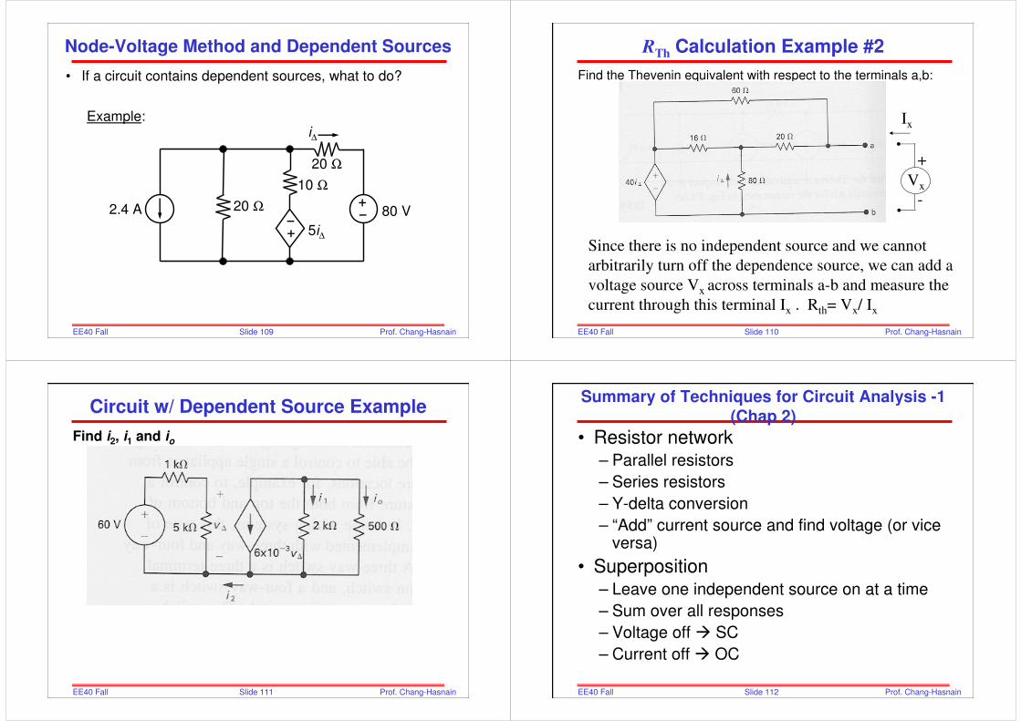
RTh Calculation Example #2
Find the Thevenin equivalent with respect to the terminals a,b:
Since there is no independent source and we cannot
arbitrarily turn off the dependence source, we can add a
voltage source Vx across terminals a-b and measure the
current through this terminal Ix . Rth= Vx/ Ix
Vx
+
-
Ix
Slide 111EE40 Fall2006
Prof. Chang-Hasnain
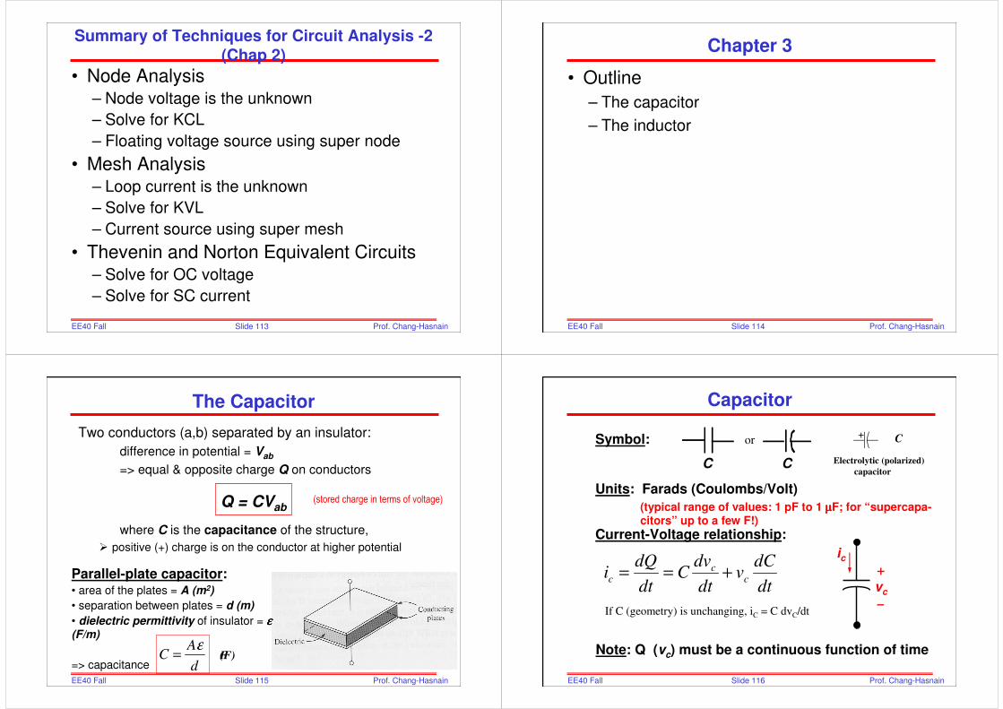
Find i2, i1 and io
Circuit w/ Dependent Source Example
Slide 112EE40 Fall2006
Prof. Chang-Hasnain
Summary of Techniques for Circuit Analysis -1 (Chap 2)
• Resistor network– Parallel resistors
– Series resistors
– Y-delta conversion
– “Add” current source and find voltage (or vice versa)
• Superposition– Leave one independent source on at a time
– Sum over all responses
– Voltage off SC
– Current off OC
Slide 113EE40 Fall2006
Prof. Chang-Hasnain
Summary of Techniques for Circuit Analysis -2 (Chap 2)
• Node Analysis– Node voltage is the unknown
– Solve for KCL
– Floating voltage source using super node
• Mesh Analysis– Loop current is the unknown
– Solve for KVL
– Current source using super mesh
• Thevenin and Norton Equivalent Circuits– Solve for OC voltage
– Solve for SC current
Slide 114EE40 Fall2006
Prof. Chang-Hasnain
Chapter 3
• Outline
– The capacitor
– The inductor
Slide 115EE40 Fall2006
Prof. Chang-Hasnain
The Capacitor
Two conductors (a,b) separated by an insulator:
difference in potential = Vab
=> equal & opposite charge Q on conductors
Q = CVab
where C is the capacitance of the structure,
positive (+) charge is on the conductor at higher potential
Parallel-plate capacitor:• area of the plates = A (m2)
• separation between plates = d (m)
• dielectric permittivity of insulator = εεεε(F/m)
=> capacitance d
AC
ε=
(stored charge in terms of voltage)
F(F)
Slide 116EE40 Fall2006
Prof. Chang-Hasnain
Symbol:
Units: Farads (Coulombs/Volt)
Current-Voltage relationship:
or
Note: Q (vc) must be a continuous function of time
Capacitor
+
vc
–
ic
dt
dCv
dt
dvC
dt
dQi c
cc +==
C C
(typical range of values: 1 pF to 1 µµµµF; for “supercapa-citors” up to a few F!)
+
Electrolytic (polarized)
capacitor
C
If C (geometry) is unchanging, iC = C dvC/dt

Slide 117EE40 Fall2006
Prof. Chang-Hasnain
Voltage in Terms of Current
)0()(1)0(
)(1
)(
)0()()(
00
0
c
t
c
t
cc
t
c
vdttiCC
Qdtti
Ctv
QdttitQ
+=+=
+=
∫∫
∫
Uses: Capacitors are used to store energy for camera flashbulbs,
in filters that separate various frequency signals, and
they appear as undesired “parasitic” elements in circuits where
they usually degrade circuit performance
Slide 118EE40 Fall2006
Prof. Chang-Hasnain
You might think the energy stored on a capacitor is QV = CV2, which has the dimension of Joules. But during
charging, the average voltage across the capacitor was only half the final value of V for a linear capacitor.
Thus, energy is .2
2
1
2
1CVQV =
Example: A 1 pF capacitance charged to 5 Volts has ½(5V)2 (1pF) = 12.5 pJ(A 5F supercapacitor charged to 5volts stores 63 J; if it discharged at aconstant rate in 1 ms energy isdischarged at a 63 kW rate!)
Stored Energy
CAPACITORS STORE ELECTRIC ENERGY
Slide 119EE40 Fall2006
Prof. Chang-Hasnain
∫=
=
=∫=
=∫
=
=
=⋅=Final
Initial
c
Final
Initial
Final
Initial
ccc
Vv
Vv
dQ vdttt
tt
dt
dQVv
Vv
vdt ivw
2CV2
12CV2
1Vv
Vv
dv Cvw InitialFinal
Final
Initial
cc −∫=
=
==
+
vc
–
ic
A more rigorous derivation
This derivation holds
independent of the circuit!
Slide 120EE40 Fall2006
Prof. Chang-Hasnain
Example: Current, Power & Energy for a Capacitor
dt
dvCi =
–+
v(t) 10 µµµµF
i(t)
t (µs)
v (V)
0 2 3 4 51
t (µs)0 2 3 4 51
1
i (µA) vc and q must be continuousfunctions of time; however,ic can be discontinuous.
)0()(1
)(0
vdiC
tv
t
+= ∫ ττ
Note: In “steady state”(dc operation), timederivatives are zero C is an open circuit
Slide 121EE40 Fall2006
Prof. Chang-Hasnain
vip =
0 2 3 4 51
w (J)
–+
v(t) 10 µµµµF
i(t)
t (µs)0 2 3 4 51
p (W)
t (µs)
2
02
1Cvpdw
t
∫ == τ
Slide 122EE40 Fall2006
Prof. Chang-Hasnain
Capacitors in Series
i(t)C1
+ v1(t) –
i(t)
+
v(t)=v1(t)+v2(t)
–
Ceq
C2
+ v2(t) –
21
111
CCCeq
+=
Slide 123EE40 Fall2006
Prof. Chang-Hasnain
Capacitive Voltage Divider
Q: Suppose the voltage applied across a series combination
of capacitors is changed by ∆v. How will this affect the voltage across each individual capacitor?
21 vvv ∆+∆=∆
v+∆∆∆∆v
C1
C2
+
v2(t)+∆∆∆∆v2
–
+
v1+∆∆∆∆v1
–+
–
Note that no net charge cancan be introduced to this node.
Therefore, −∆Q1+∆Q2=0
Q1+∆∆∆∆Q1
-Q1−−−−∆∆∆∆Q1
Q2+∆∆∆∆Q2
−−−−Q2−−−−∆∆∆∆Q2
∆Q1=C1∆v1
∆Q2=C2∆v2
2211 vCvC ∆=∆⇒
vCC
Cv ∆
+=∆
21
12
Note: Capacitors in series have the same incremental
charge.Slide 124EE40 Fall
2006Prof. Chang-Hasnain
Symbol:
Units: Henrys (Volts • second / Ampere)
Current in terms of voltage:
Note: iL must be a continuous function of time
Inductor
+
vL
–
iL
∫ +=
=
t
t
LL
LL
tidvL
ti
dttvL
di
0
)()(1
)(
)(1
0ττ
L
(typical range of values: µµµµH to 10 H)

Slide 125EE40 Fall2006
Prof. Chang-Hasnain
Stored Energy
Consider an inductor having an initial current i(t0) = i0
2
0
2
2
1
2
1)(
)()(
)()()(
0
LiLitw
dptw
titvtp
t
t
−=
==
==
∫ ττ
INDUCTORS STORE MAGNETIC ENERGY
Slide 126EE40 Fall2006
Prof. Chang-Hasnain
Inductors in Series and Parallel
Common
Current
Common
Voltage
Slide 127EE40 Fall2006
Prof. Chang-Hasnain
Capacitor
v cannot change instantaneously
i can change instantaneously
Do not short-circuit a chargedcapacitor (-> infinite current!)
n cap.’s in series:
n cap.’s in parallel:
In steady state (not time-varying), a capacitor behaves like an open
circuit.
Inductor
i cannot change instantaneously
v can change instantaneously
Do not open-circuit an inductor with current (-> infinite voltage!)
n ind.’s in series:
n ind.’s in parallel:
In steady state, an inductor
behaves like a short circuit.
Summary
∑
∑
=
=
=
=
n
i
ieq
n
i ieq
CC
CC
1
1
11
21;
2
dvi C w Cv
dt= = 21
;2
div L w Li
dt= =
∑
∑
=
=
=
=
n
i ieq
n
i
ieq
LL
LL
1
1
11
Slide 128EE40 Fall2006
Prof. Chang-Hasnain
Chapter 4
• OUTLINE
– First Order Circuits
• RC and RL Examples
• General Procedure
– RC and RL Circuits with General Sources
• Particular and complementary solutions
• Time constant
– Second Order Circuits
• The differential equation
• Particular and complementary solutions
• The natural frequency and the damping ratio
• Reading
– Chapter 4
Slide 129EE40 Fall2006
Prof. Chang-Hasnain
First-Order Circuits
• A circuit that contains only sources, resistors
and an inductor is called an RL circuit.
• A circuit that contains only sources, resistors
and a capacitor is called an RC circuit.
• RL and RC circuits are called first-order circuits
because their voltages and currents are
described by first-order differential equations.
–+
vs L
R
–+
vs C
R
i i
Slide 130EE40 Fall2006
Prof. Chang-Hasnain
Response of a Circuit
• Transient response of an RL or RC circuit is
– Behavior when voltage or current source are suddenlyapplied to or removed from the circuit due to switching.
– Temporary behavior
• Steady-state response (aka. forced response)
– Response that persists long after transient has decayed
• Natural response of an RL or RC circuit is
– Behavior (i.e., current and voltage) when stored energy
in the inductor or capacitor is released to the resistive part of the network (containing no independent
sources).
Slide 131EE40 Fall2006
Prof. Chang-Hasnain
Natural Response Summary
RL Circuit
• Inductor currentcannot change instantaneously
• In steady state, an inductor behaves like a short circuit.
RC Circuit
• Capacitor voltagecannot change instantaneously
• In steady state, a capacitor behaves like an open circuit
R
i
L
+
v
–
RC
Slide 132EE40 Fall2006
Prof. Chang-Hasnain
First Order Circuits
( )( ) ( )c
c s
dv tRC v t v t
dt+ =
KVL around the loop:
vr(t) + vc(t) = vs(t))()(
1)(tidxxv
LR
tvs
t
=+ ∫∞−
KCL at the node:
( )( ) ( )L
L s
di tLi t i t
R dt+ =
R+
-Cvs(t)
+
-vc(t)
+ -vr(t)
ic(t)
vL(t)is(t)R L
+
-
iL(t)
Slide 133EE40 Fall2006
Prof. Chang-Hasnain
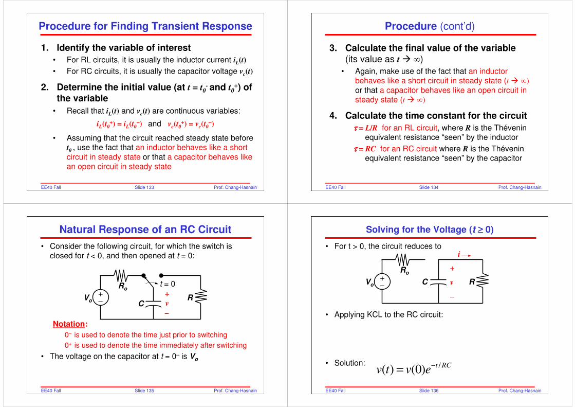
Procedure for Finding Transient Response
1. Identify the variable of interest
• For RL circuits, it is usually the inductor current iL(t)
• For RC circuits, it is usually the capacitor voltage vc(t)
2. Determine the initial value (at t = t0- and t0
+) of the variable
• Recall that iL(t) and vc(t) are continuous variables:
iL(t0+) = iL(t0
−−−−) and vc(t0+) = vc(t0
−−−−)
• Assuming that the circuit reached steady state before t0 , use the fact that an inductor behaves like a short
circuit in steady state or that a capacitor behaves like
an open circuit in steady state
Slide 134EE40 Fall2006
Prof. Chang-Hasnain
Procedure (cont’d)
3. Calculate the final value of the variable (its value as t ∞)
• Again, make use of the fact that an inductor behaves like a short circuit in steady state (t ∞)
or that a capacitor behaves like an open circuit in steady state (t ∞)
4. Calculate the time constant for the circuit
ττττ = L/R for an RL circuit, where R is the Théveninequivalent resistance “seen” by the inductor
ττττ = RC for an RC circuit where R is the Théveninequivalent resistance “seen” by the capacitor
Slide 135EE40 Fall2006
Prof. Chang-Hasnain
• Consider the following circuit, for which the switch is closed for t < 0, and then opened at t = 0:
Notation:
0– is used to denote the time just prior to switching
0+ is used to denote the time immediately after switching
• The voltage on the capacitor at t = 0– is Vo
Natural Response of an RC Circuit
C
Ro
RVo
t = 0
+−
+
v
–
Slide 136EE40 Fall2006
Prof. Chang-Hasnain
Solving for the Voltage (t ≥≥≥≥ 0)
• For t > 0, the circuit reduces to
• Applying KCL to the RC circuit:
• Solution:
+
v
–
RCtevtv
/)0()( −=
C
Ro
RVo+−
i
Slide 137EE40 Fall2006
Prof. Chang-Hasnain
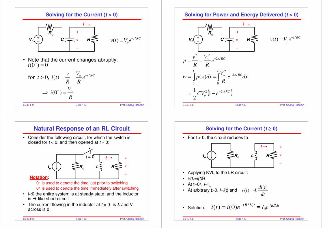
Solving for the Current (t > 0)
• Note that the current changes abruptly:
RCt
oeVtv /)( −=
R
Vi
eR
V
R
vtit
i
o
RCto
=⇒
==>
=
+
−
−
)0(
)( 0,for
0)0(
/
+
v
–
C
Ro
RVo+−
i
Slide 138EE40 Fall2006
Prof. Chang-Hasnain
Solving for Power and Energy Delivered (t > 0)
( )RCt
o
t
RCxo
t
RCto
eCV
dxeR
Vdxxpw
eR
V
R
vp
/22
0
/22
0
/222
12
1
)(
−
−
−
−=
==
==
∫∫
RCt
oeVtv/)( −=
+
v
–
C
Ro
RVo+−
i
Slide 139EE40 Fall2006
Prof. Chang-Hasnain
Natural Response of an RL Circuit
• Consider the following circuit, for which the switch is closed for t < 0, and then opened at t = 0:
Notation:
0– is used to denote the time just prior to switching
0+ is used to denote the time immediately after switching
• t<0 the entire system is at steady-state; and the inductor is like short circuit
• The current flowing in the inductor at t = 0– is Io and V across is 0.
LRo RIo
t = 0 i +
v
–
Slide 140EE40 Fall2006
Prof. Chang-Hasnain
Solving for the Current (t ≥≥≥≥ 0)
• For t > 0, the circuit reduces to
• Applying KVL to the LR circuit:
• v(t)=i(t)R
• At t=0+, i=I0,
• At arbitrary t>0, i=i(t) and
• Solution:
( )( )
di tv t L
dt=
LRo RIo
i +
v
–
= I0e-(R/L)ttLR
eiti)/()0()( −=
-
Slide 141EE40 Fall2006
Prof. Chang-Hasnain
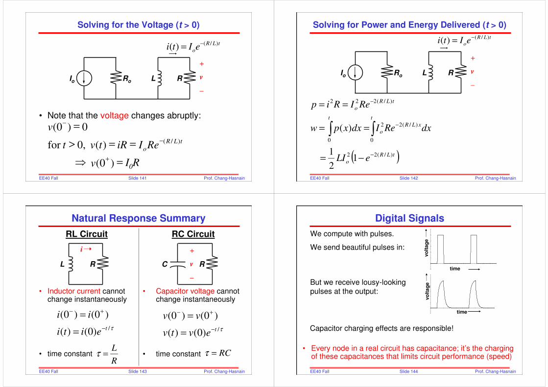
Solving for the Voltage (t > 0)
• Note that the voltage changes abruptly:
tLR
oeIti)/()( −=
LRo RIo
+
v
–
I0Rv
ReIiRtvt
v
tLR
o
=⇒
==>
=
+
−
−
)0(
)(0,for
0)0(
)/(
Slide 142EE40 Fall2006
Prof. Chang-Hasnain
Solving for Power and Energy Delivered (t > 0)
tLR
oeIti)/()( −=
LRo RIo
+
v
–
( )tLR
o
t
xLR
o
t
tLR
o
eLI
dxReIdxxpw
ReIRip
)/(22
0
)/(22
0
)/(222
12
1
)(
−
−
−
−=
==
==
∫∫
Slide 143EE40 Fall2006
Prof. Chang-Hasnain
Natural Response Summary
RL Circuit
• Inductor current cannot change instantaneously
• time constant
RC Circuit
• Capacitor voltage cannot change instantaneously
• time constantR
L=τ
τ/)0()(
)0()0(
teiti
ii
−
+−
=
=
R
i
L
+
v
–
RC
τ/)0()(
)0()0(
tevtv
vv
−
+−
=
=
RC=τ
Slide 144EE40 Fall2006
Prof. Chang-Hasnain
• Every node in a real circuit has capacitance; it’s the charging of these capacitances that limits circuit performance (speed)
We compute with pulses.
We send beautiful pulses in:
But we receive lousy-looking
pulses at the output:
Capacitor charging effects are responsible!
time
vo
lta
ge
time
vo
lta
ge
Digital Signals

Slide 145EE40 Fall2006
Prof. Chang-Hasnain
Circuit Model for a Logic Gate
• Recall (from Lecture 1) that electronic building blocks referred to as “logic gates” are used to implement logical functions (NAND, NOR, NOT) in digital ICs
– Any logical function can be implemented using these gates.
• A logic gate can be modeled as a simple RC circuit:
+
Vout
–
R
Vin(t) +− C
switches between “low” (logic 0) and “high” (logic 1) voltage states
Slide 146EE40 Fall2006
Prof. Chang-Hasnain
The input voltage pulse width must be large
enough; otherwise the
output pulse is distorted.
(We need to wait for the output to reach a recognizable logic level, before changing the input again.)
0
1
2
3
4
5
6
0 1 2 3 4 5
Time
Vo
ut
Pulse width = 0.1RC
0
1
2
3
4
5
6
0 1 2 3 4 5
Time
Vo
ut
0
1
2
3
4
5
6
0 5 10 15 20 25
Time
Vo
ut
Pulse Distortion
+
Vout
–
R
Vin(t) C
+
–
Pulse width = 10RCPulse width = RC
Slide 147EE40 Fall2006
Prof. Chang-Hasnain
Vin
RVout
C
Suppose a voltage pulse of width
5 µs and height 4 V is applied to theinput of this circuit beginning at t = 0:
R = 2.5 kΩ
C = 1 nF
• First, Vout will increase exponentially toward 4 V.
• When Vin goes back down, Vout will decrease exponentially back down to 0 V.
What is the peak value of Vout?
The output increases for 5 µs, or 2 time constants.
It reaches 1-e-2 or 86% of the final value.
0.86 x 4 V = 3.44 V is the peak value
Example
τ = RC = 2.5 µs
Slide 148EE40 Fall2006
Prof. Chang-Hasnain
First Order Circuits: Forced Response
( )( ) ( )c
c s
dv tRC v t v t
dt+ =
KVL around the loop:
vr(t) + vc(t) = vs(t))()(
1)(tidxxv
LR
tvs
t
=+ ∫∞−
KCL at the node:
( )( ) ( )L
L s
di tLi t i t
R dt+ =
R+
-Cvs(t)
+
-vc(t)
+ -vr(t)
ic(t)
vL(t)is(t)R L
+
-
iL(t)
Slide 149EE40 Fall2006
Prof. Chang-Hasnain
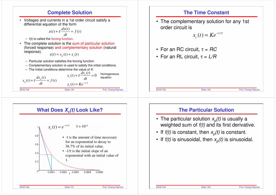
Complete Solution
• Voltages and currents in a 1st order circuit satisfy a differential equation of the form
– f(t) is called the forcing function.
• The complete solution is the sum of particular solution(forced response) and complementary solution (natural response).
– Particular solution satisfies the forcing function
– Complementary solution is used to satisfy the initial conditions.
– The initial conditions determine the value of K.
( )( ) ( )
dx tx t f t
dtτ+ =
/
( )( ) 0
( )
cc
t
c
dx tx t
dt
x t Keτ
τ
−
+ =
=
( )( ) ( )
p
p
dx tx t f t
dtτ+ =
Homogeneous
equation
( ) ( ) ( )p cx t x t x t= +
Slide 150EE40 Fall2006
Prof. Chang-Hasnain
The Time Constant
• The complementary solution for any 1st order circuit is
• For an RC circuit, τ = RC
• For an RL circuit, τ = L/R
/( ) t
cx t Ke τ−=
Slide 151EE40 Fall2006
Prof. Chang-Hasnain
What Does Xc(t) Look Like?
τ = 10-4/( ) t
cx t e τ−=
• τ is the amount of time necessary
for an exponential to decay to
36.7% of its initial value.
• -1/τ is the initial slope of an
exponential with an initial value of
1.
Slide 152EE40 Fall2006
Prof. Chang-Hasnain
The Particular Solution
• The particular solution xp(t) is usually a weighted sum of f(t) and its first derivative.
• If f(t) is constant, then xp(t) is constant.
• If f(t) is sinusoidal, then xp(t) is sinusoidal.
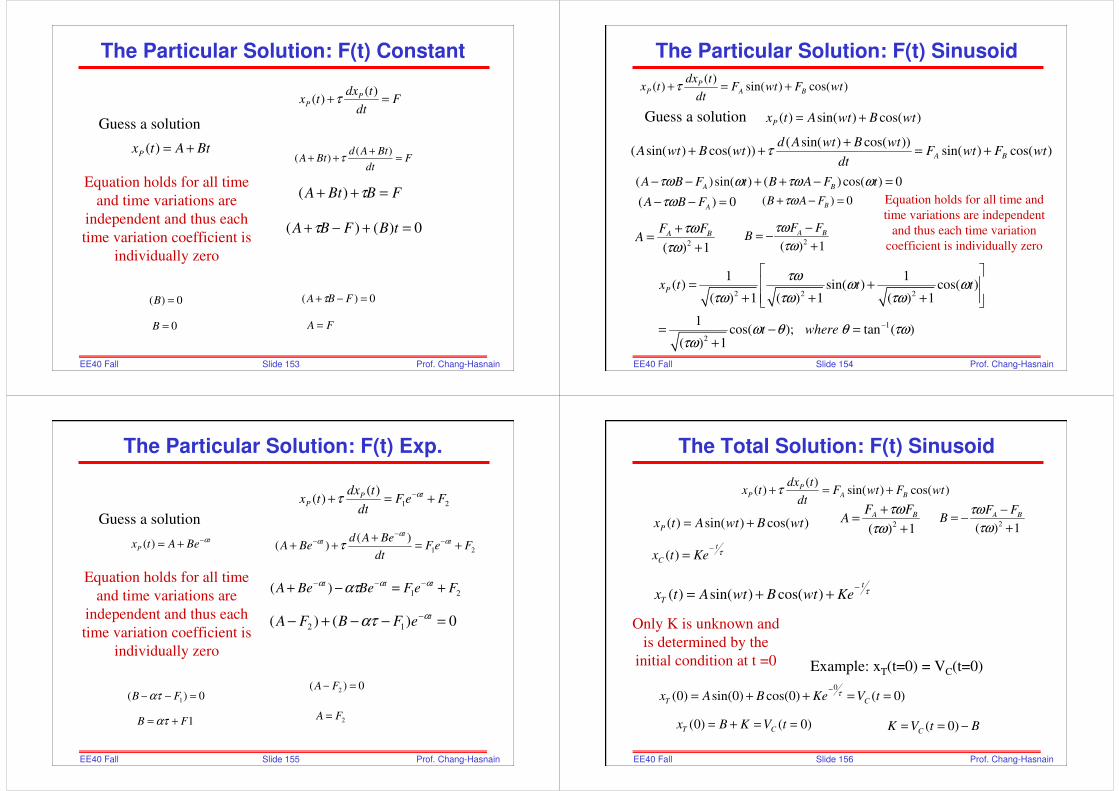
Slide 153EE40 Fall2006
Prof. Chang-Hasnain
The Particular Solution: F(t) Constant
BtAtxP +=)(
Fdt
tdxtx P
P =+)(
)( τ
Fdt
BtAdBtA =
+++
)()( τ
FBBtA =++ τ)(
0)()( =+−+ tBFBA τ
0)( =B 0)( =−+ FBA τ
FA =
Guess a solution
0=B
Equation holds for all time
and time variations are
independent and thus each
time variation coefficient is
individually zero
Slide 154EE40 Fall2006
Prof. Chang-Hasnain
The Particular Solution: F(t) Sinusoid
)cos()sin()( wtBwtAtxP +=
)cos()sin()(
)( wtFwtFdt
tdxtx BA
PP +=+τ
)cos()sin())cos()sin((
))cos()sin(( wtFwtFdt
wtBwtAdwtBwtA BA +=
+++ τ
Guess a solution
Equation holds for all time and
time variations are independent
and thus each time variation
coefficient is individually zero
( )sin( ) ( ) cos( ) 0A B
A B F t B A F tτω ω τω ω− − + + − =
( ) 0BB A Fτω+ − =( ) 0AA B Fτω− − =
2( ) 1
A BF FA
τω
τω
+=
+2( ) 1
A BF FB
τω
τω
−= −
+
2 2 2
1
2
1 1( ) sin( ) cos( )
( ) 1 ( ) 1 ( ) 1
1cos( ); tan ( )
( ) 1
Px t t t
t where
τωω ω
τω τω τω
ω θ θ τωτω
−
= +
+ + +
= − =+
Slide 155EE40 Fall2006
Prof. Chang-Hasnain
The Particular Solution: F(t) Exp.
t
P BeAtxα−+=)(
21
)()( FeF
dt
tdxtx
tPP +=+ −ατ
21
)()( FeF
dt
BeAdBeA
tt
t +=+
++ −−
− αα
α τ
21)( FeFBeBeA ttt +=−+ −−− ααα ατ
0)()( 12 =−−+− − teFBFA
αατ
0)( 1 =−− FB ατ0)( 2 =− FA
2FA =
Guess a solution
1FB += ατ
Equation holds for all time
and time variations are
independent and thus each
time variation coefficient is
individually zero
Slide 156EE40 Fall2006
Prof. Chang-Hasnain
The Total Solution: F(t) Sinusoid
)cos()sin()( wtBwtAtxP +=
)cos()sin()(
)( wtFwtFdt
tdxtx BA
PP +=+τ
τt
T KewtBwtAtx−
++= )cos()sin()(
Only K is unknown and
is determined by the
initial condition at t =0
τt
C Ketx−
=)(
Example: xT(t=0) = VC(t=0)
)0()0cos()0sin()0(0
==++=−
tVKeBAx CTτ
)0()0( ==+= tVKBx CT BtVK C −== )0(
2( ) 1
A BF FA
τω
τω
+=
+ 2( ) 1
A BF FB
τω
τω
−= −
+

Slide 157EE40 Fall2006
Prof. Chang-Hasnain
Example
• Given vc(0-)=1, Vs=2 cos(ωt), ω=200.
• Find i(t), vc(t)=?
C
R
Vs
t = 0
+−
+
vc
–
Slide 158EE40 Fall2006
Prof. Chang-Hasnain
2nd Order Circuits
• Any circuit with a single capacitor, a single inductor, an arbitrary number of sources, and an arbitrary number of resistors is a circuit of order 2.
• Any voltage or current in such a circuit is the solution to a 2nd order differential equation.
Slide 159EE40 Fall2006
Prof. Chang-Hasnain
A 2nd Order RLC Circuit
R+
-Cvs(t)
i (t)
L
• Application: Filters
– A bandpass filter such as the IF amp for the AM radio.
– A lowpass filter with a sharper cutoff than can be obtained with an RC circuit.
Slide 160EE40 Fall2006
Prof. Chang-Hasnain
The Differential Equation
KVL around the loop:
vr(t) + vc(t) + vl(t) = vs(t)
i (t)
R+
-Cvs(t)
+
-
vc(t)
+ -vr(t)
L
+- vl(t)
1 ( )( ) ( ) ( )
t
s
di tRi t i x dx L v t
C dt−∞
+ + =∫2
2
( )( ) 1 ( ) 1( ) s
dv tR di t d i ti t
L dt LC dt L dt+ + =
Slide 161EE40 Fall2006
Prof. Chang-Hasnain
The Differential Equation
The voltage and current in a second order circuit is
the solution to a differential equation of the
following form:
Xp(t) is the particular solution (forced response)
and Xc(t) is the complementary solution (natural
response).
22
02
( ) ( )2 ( ) ( )
d x t dx tx t f t
dt dtα ω+ + =
( ) ( ) ( )p cx t x t x t= +
Slide 162EE40 Fall2006
Prof. Chang-Hasnain
The Particular Solution
• The particular solution xp(t) is usually a weighted sum of f(t) and its first and second derivatives.
• If f(t) is constant, then xp(t) is constant.
• If f(t) is sinusoidal, then xp(t) is sinusoidal.
Slide 163EE40 Fall2006
Prof. Chang-Hasnain
The Complementary Solution
The complementary solution has the following form:
K is a constant determined by initial conditions.
s is a constant determined by the coefficients of the differential equation.
( ) st
cx t Ke=
22
022 0
st ststd Ke dKe
Kedt dt
α ω+ + =
2 2
02 0st st sts Ke sKe Keα ω+ + =
2 2
02 0s sα ω+ + =
Slide 164EE40 Fall2006
Prof. Chang-Hasnain
Characteristic Equation
• To find the complementary solution, we need to solve the characteristic equation:
• The characteristic equation has two roots-call them s1 and s2.
2 2
0 0
0
2 0s sζω ω
α ζω
+ + =
=
1 2
1 2( )s t s t
cx t K e K e= +
2
1 0 0 1s ζω ω ζ= − + −
2
2 0 0 1s ζω ω ζ= − − −

Slide 165EE40 Fall2006
Prof. Chang-Hasnain
Damping Ratio and Natural Frequency
• The damping ratio determines what type of
solution we will get:
– Exponentially decreasing (ζ >1)
– Exponentially decreasing sinusoid (ζ < 1)
• The natural frequency is ω0
– It determines how fast sinusoids wiggle.
0
αζ
ω=
2
1 0 0 1s ζω ω ζ= − + −
2
2 0 0 1s ζω ω ζ= − − −damping ratio
Slide 166EE40 Fall2006
Prof. Chang-Hasnain
Overdamped : Real Unequal Roots
• If ζ > 1, s1 and s2 are real and not equal.
tt
c eKeKti
−−−
−+−
+=1
2
1
1
200
200
)(ςωςωςωςω
0
0.2
0.4
0.6
0.8
1
-1.00E-06
t
i(t)
-0.2
0
0.2
0.4
0.6
0.8
-1.00E-06
t
i(t)
Slide 167EE40 Fall2006
Prof. Chang-Hasnain
Underdamped: Complex Roots
• If ζ < 1, s1 and s2 are complex.
• Define the following constants:
( )1 2( ) cos sint
c d dx t e A t A tα ω ω−= +
0α ζω= 2
0 1dω ω ζ= −
-1
-0.8
-0.6
-0.4
-0.2
0
0.2
0.4
0.6
0.8
1
-1.00E-05 1.00E-05 3.00E-05
t
i(t)
Slide 168EE40 Fall2006
Prof. Chang-Hasnain
Critically damped: Real Equal Roots
• If ζ = 1, s1 and s2 are real and equal.
0 0
1 2( )t t
cx t K e K te
ςω ςω− −= +
Note: The
degeneracy of the
roots results in the
extra factor of ‘t’
Slide 169EE40 Fall2006
Prof. Chang-Hasnain
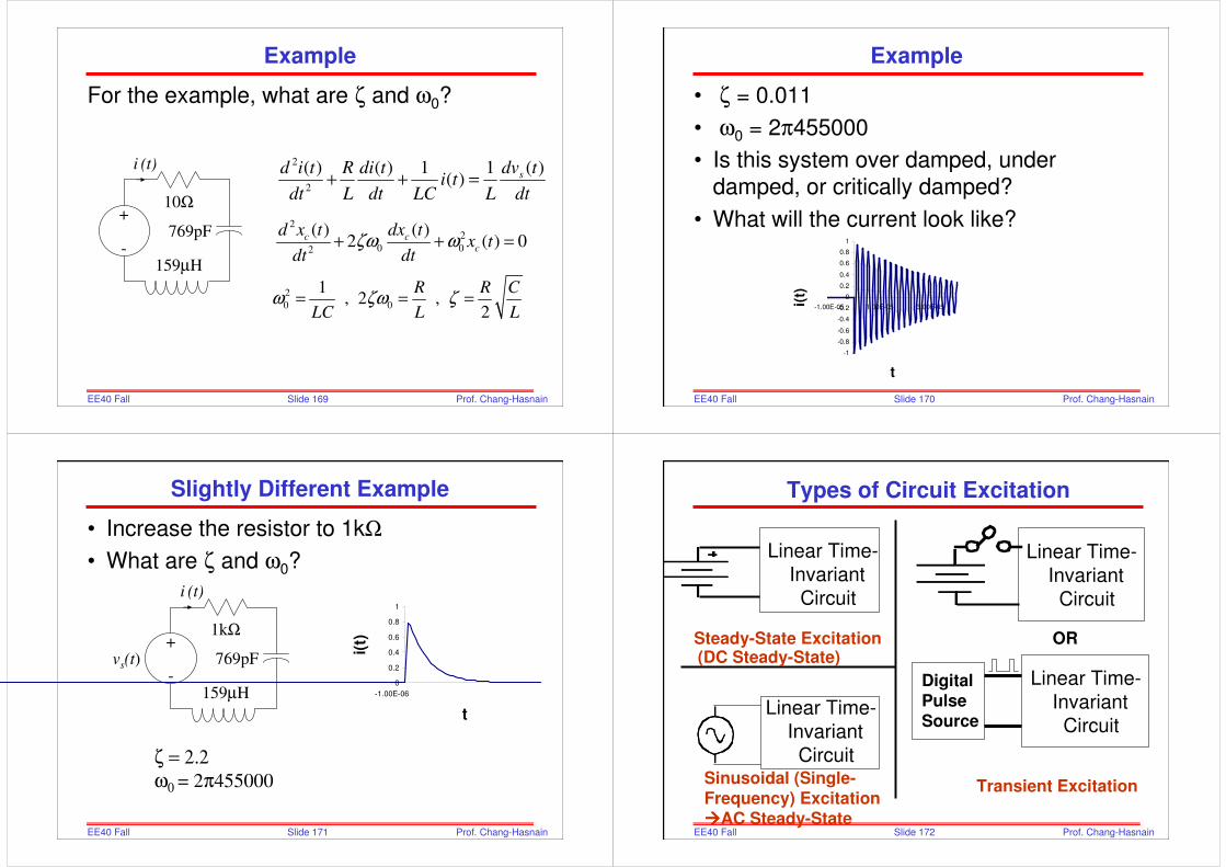
Example
For the example, what are ζ and ω0?
dt
tdv
Lti
LCdt
tdi
L
R
dt
tid s )(1)(
1)()(2
2
=++
22
0 02
( ) ( )2 ( ) 0c c
c
d x t dx tx t
dt dtζω ω+ + =
2
0 0
1, 2 ,
2
R R C
LC L Lω ζω ζ= = =
10Ω+
-769pF
i (t)
159µH
Slide 170EE40 Fall2006
Prof. Chang-Hasnain
Example
• ζ = 0.011
• ω0 = 2π455000
• Is this system over damped, under damped, or critically damped?
• What will the current look like?
-1
-0.8
-0.6
-0.4
-0.2
0
0.2
0.4
0.6
0.8
1
-1.00E-05 1.00E-05 3.00E-05
t
i(t)
Slide 171EE40 Fall2006
Prof. Chang-Hasnain
Slightly Different Example
• Increase the resistor to 1kΩ
• What are ζ and ω0?
1kΩ+
-769pFvs(t)
i (t)
159µH
ζ = 2.2ω0 = 2π455000
0
0.2
0.4
0.6
0.8
1
-1.00E-06
t
i(t)
Slide 172EE40 Fall2006
Prof. Chang-Hasnain
Types of Circuit Excitation
Linear Time-
Invariant
Circuit
Steady-State Excitation
Linear Time-
Invariant
Circuit
OR
Linear Time-
Invariant
Circuit
DigitalPulseSource
Transient Excitation
Linear Time-
Invariant
CircuitSinusoidal (Single-Frequency) ExcitationAC Steady-State
(DC Steady-State)
Slide 173EE40 Fall2006
Prof. Chang-Hasnain
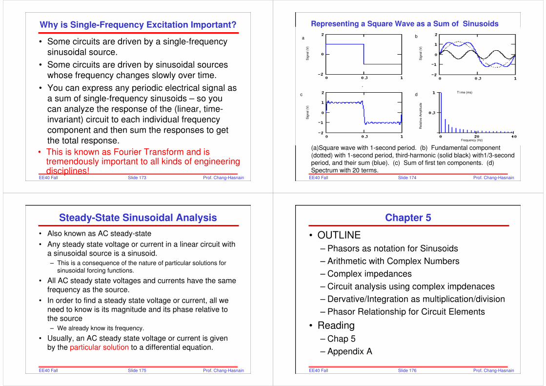
Why is Single-Frequency Excitation Important?
• Some circuits are driven by a single-frequency
sinusoidal source.
• Some circuits are driven by sinusoidal sources
whose frequency changes slowly over time.
• You can express any periodic electrical signal as
a sum of single-frequency sinusoids – so you
can analyze the response of the (linear, time-
invariant) circuit to each individual frequency
component and then sum the responses to get
the total response.
• This is known as Fourier Transform and is tremendously important to all kinds of engineering disciplines!
Slide 174EE40 Fall2006
Prof. Chang-Hasnain
a b
c d
sig
nal
sig
nal
T i me (ms)
Frequency (Hz)
Sig
nal (V
)
Re
lative
Am
plit
ud
e
Sig
nal (V
)
Sig
nal (V
)
Representing a Square Wave as a Sum of Sinusoids
(a)Square wave with 1-second period. (b) Fundamental component (dotted) with 1-second period, third-harmonic (solid black) with1/3-second period, and their sum (blue). (c) Sum of first ten components. (d) Spectrum with 20 terms.
Slide 175EE40 Fall2006
Prof. Chang-Hasnain
Steady-State Sinusoidal Analysis
• Also known as AC steady-state
• Any steady state voltage or current in a linear circuit with
a sinusoidal source is a sinusoid.
– This is a consequence of the nature of particular solutions for sinusoidal forcing functions.
• All AC steady state voltages and currents have the same
frequency as the source.
• In order to find a steady state voltage or current, all we
need to know is its magnitude and its phase relative to the source
– We already know its frequency.
• Usually, an AC steady state voltage or current is given
by the particular solution to a differential equation.
Slide 176EE40 Fall2006
Prof. Chang-Hasnain
Chapter 5
• OUTLINE
– Phasors as notation for Sinusoids
– Arithmetic with Complex Numbers
– Complex impedances
– Circuit analysis using complex impdenaces
– Dervative/Integration as multiplication/division
– Phasor Relationship for Circuit Elements
• Reading
– Chap 5
– Appendix A
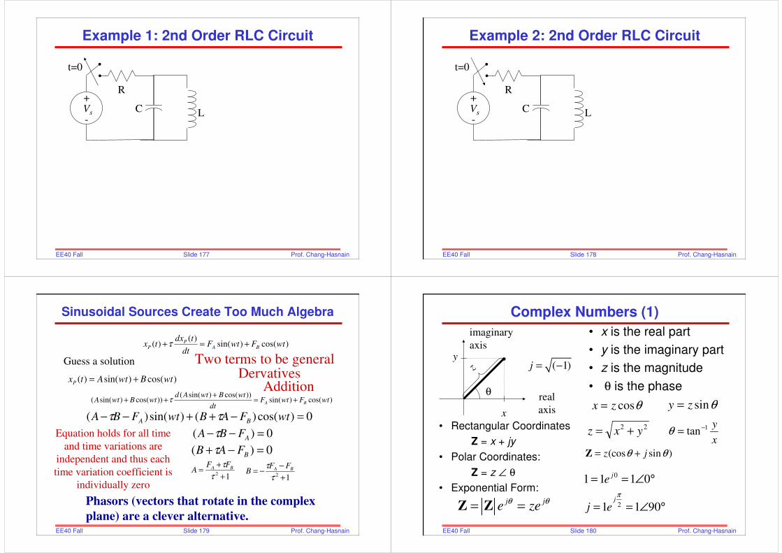
Slide 177EE40 Fall2006
Prof. Chang-Hasnain
Example 1: 2nd Order RLC Circuit
R+
-CVs L
t=0
Slide 178EE40 Fall2006
Prof. Chang-Hasnain
Example 2: 2nd Order RLC Circuit
R+
-CVs L
t=0
Slide 179EE40 Fall2006
Prof. Chang-Hasnain
Sinusoidal Sources Create Too Much Algebra
)cos()sin()( wtBwtAtxP +=
)cos()sin()(
)( wtFwtFdt
tdxtx BA
PP +=+τ
)cos()sin())cos()sin((
))cos()sin(( wtFwtFdt
wtBwtAdwtBwtA BA +=
+++ τ
Guess a solution
Equation holds for all time
and time variations are
independent and thus each
time variation coefficient is
individually zero
0)cos()()sin()( =−++−− wtFABwtFBA BA ττ
0)( =−+ BFAB τ
0)( =−− AFBA τ
12 +
+=
τ
τ BA FFA
12 +
−−=
τ
τ BA FFB
DervativesAddition
Two terms to be general
Phasors (vectors that rotate in the complex
plane) are a clever alternative.Slide 180EE40 Fall
2006Prof. Chang-Hasnain
Complex Numbers (1)
• x is the real part
• y is the imaginary part
• z is the magnitude
• θ is the phase
( 1)j = −
θ
z
x
y
real
axis
imaginary
axis
• Rectangular Coordinates
Z = x + jy
• Polar Coordinates:
Z = z ∠ θ
• Exponential Form:
θcoszx = θsinzy =
22yxz +=
x
y1tan−=θ
(cos sin )z jθ θ= +Z
j je ze
θ θ= =Z Z
0
2
1 1 1 0
1 1 90
j
j
e
j eπ
= = ∠ °
= = ∠ °
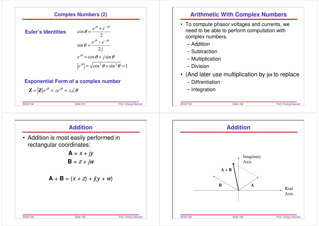
Slide 181EE40 Fall2006
Prof. Chang-Hasnain
Complex Numbers (2)
2 2
cos2
sin2
cos sin
cos sin 1
j j
j j
j
j
e e
e e
j
e j
e
θ θ
θ θ
θ
θ
θ
θ
θ θ
θ θ
−
−
+=
−=
= +
= + =
j je ze z
θ θ θ= = = ∠Z Z
Euler’s Identities
Exponential Form of a complex number
Slide 182EE40 Fall2006
Prof. Chang-Hasnain
Arithmetic With Complex Numbers
• To compute phasor voltages and currents, we
need to be able to perform computation with
complex numbers.
– Addition
– Subtraction
– Multiplication
– Division
• (And later use multiplication by jω to replace
– Diffrentiation
– Integration
Slide 183EE40 Fall2006
Prof. Chang-Hasnain
Addition
• Addition is most easily performed in rectangular coordinates:
A = x + jy
B = z + jw
A + B = (x + z) + j(y + w)
Slide 184EE40 Fall2006
Prof. Chang-Hasnain
Addition
Real
Axis
Imaginary
Axis
AB
A + B
Slide 185EE40 Fall2006
Prof. Chang-Hasnain
Subtraction
• Subtraction is most easily performed in rectangular coordinates:
A = x + jy
B = z + jw
A - B = (x - z) + j(y - w)
Slide 186EE40 Fall2006
Prof. Chang-Hasnain
Subtraction
Real
Axis
Imaginary
Axis
AB
A - B
Slide 187EE40 Fall2006
Prof. Chang-Hasnain
Multiplication
• Multiplication is most easily performed in polar coordinates:
A = AM ∠ θ
B = BM ∠ φ
A × B = (AM × BM) ∠ (θ + φ)
Slide 188EE40 Fall2006
Prof. Chang-Hasnain
Multiplication
Real
Axis
Imaginary
Axis
A
BA × B

Slide 189EE40 Fall2006
Prof. Chang-Hasnain
Division
• Division is most easily performed in polar coordinates:
A = AM ∠ θ
B = BM ∠ φ
A / B = (AM / BM) ∠ (θ − φ)
Slide 190EE40 Fall2006
Prof. Chang-Hasnain
Division
Real
Axis
Imaginary
Axis
A
B
A / B
Slide 191EE40 Fall2006
Prof. Chang-Hasnain
Arithmetic Operations of Complex Numbers
• Add and Subtract: it is easiest to do this in rectangular format
– Add/subtract the real and imaginary parts separately
• Multiply and Divide: it is easiest to do this in
exponential/polar format
– Multiply (divide) the magnitudes
– Add (subtract) the phases
1
2
1 2
1 1 1 1 1 1 1
2 2 2 2 2 2 2 2
2 1 1 2 2 1 1 2 2
2 1 1 2 2 1 1 2 2
( )
2 1 2 1 2 1 2
2 1 2
cos sin
cos sin
( cos cos ) ( sin sin )
( cos cos ) ( sin sin )
( ) ( ) ( )
/ ( / )
j
j
j
z e z z jz
z e z z jz
z z j z z
z z j z z
z z e z z
z z e
θ
θ
θ θ
θ θ θ
θ θ θ
θ θ θ θ
θ θ θ θ
θ θ+
= = ∠ = +
= = ∠ = +
+ = + + +
− = − + −
× = × = × ∠ +
=
1
1
1
1
1
Z
Z
Z Z
Z Z
Z Z
Z Z 1 2( )
1 2 1 2( / ) ( )j
z zθ θ θ θ− = ∠ −
Slide 192EE40 Fall2006
Prof. Chang-Hasnain
Phasors
• Assuming a source voltage is a sinusoid time-
varying function
v(t) = V cos (ωt + θ)
• We can write:
• Similarly, if the function is v(t) = V sin (ωt + θ)
( ) ( )( ) cos( ) Re Rej t j t
j
v t V t V e Ve
Define Phasor as Ve V
ω θ ω θ
θ
ω θ
θ
+ + = + = =
= ∠
( )
( )2
2
( ) sin( ) cos( ) Re2
j t
v t V t V t Ve
Phasor V
πω θ
πθ
πω θ ω θ
+ −
−
= + = + − =
= ∠
Slide 193EE40 Fall2006
Prof. Chang-Hasnain
Phasor: Rotating Complex Vector
Real
Axis
Imaginary
Axis
V
)( tjjwtj eeVetVtv ωφφω VReRe)cos()( ==+=
Rotates at uniform
angular velocity ωt
cos(ωωωωt+φφφφ)
The head start angle is φφφφ.
Slide 194EE40 Fall2006
Prof. Chang-Hasnain
Complex Exponentials
• We represent a real-valued sinusoid as the real part of a complex exponential after multiplying by .
• Complex exponentials – provide the link between time functions and phasors.
– Allow dervatives and integrals to be replaced by multiplying or dividing by jω
– make solving for AC steady state simple algebra with complex numbers.
• Phasors allow us to express current-voltage relationships for inductors and capacitors much like we express the current-voltage relationship for a resistor.
tje
ω
Slide 195EE40 Fall2006
Prof. Chang-Hasnain
I-V Relationship for a Capacitor
Suppose that v(t) is a sinusoid:
v(t) = ReVM ej(ωt+θ)
Find i(t).
C v(t)
+
-
i(t)
dt
tdvCti
)()( =
Slide 196EE40 Fall2006
Prof. Chang-Hasnain
Capacitor Impedance (1)
C v(t
)
+
-
i(t)
dt
tdvCti
)()( =
( ) ( )
( ) ( ) ( ) ( )
( ) ( )
( ) cos( )2
( )( )
2 2
sin( ) cos( )2 2
(
2
j t j t
j t j t j t j t
j t j t
c
Vv t V t e e
dv t CV d CVi t C e e j e e
dt dt
CVe e CV t CV t
j
V VZ
CVI
ω θ ω θ
ω θ ω θ ω θ ω θ
ω θ ω θ
ω θ
ω
ω πω ω θ ω ω θ
θθ θ
π ωθ
+ − +
+ − + + − +
+ − +
= + = +
= = + = −
− = − = − + = + +
∠= = = ∠ −
∠ +
V
I
1 1 1) ( )
2 2j
C C j C
π π
ω ω ω− = ∠ − = − =

Slide 197EE40 Fall2006
Prof. Chang-Hasnain
Capacitor Impedance (2)
C v(t
)
+
-
i(t)
dt
tdvCti
)()( =
( )
( )( )
( ) cos( ) Re
( )( ) Re Re
1( )
j t
j tj t
c
v t V t Ve V
dv t dei t C CV j CVe I
dt dt
V VZ
I j CV j C
ω θ
ω θω θ
ω θ θ
ω θ
θθ θ
θ ω ω
+
++
⇒
⇒
= + = = ∠
= = = = ∠
∠= = = ∠ − =
∠
V
I
V
I
Phasor definition
Slide 198EE40 Fall2006
Prof. Chang-Hasnain
Example
v(t) = 120V cos(377t + 30°)
C = 2µF
• What is V?
• What is I?
• What is i(t)?
Slide 199EE40 Fall2006
Prof. Chang-Hasnain
Computing the Current
ωjdt
d⇒
Note: The differentiation and integration
operations become algebraic operations
ωjdt
1⇒∫
Slide 200EE40 Fall2006
Prof. Chang-Hasnain
Inductor Impedance
V = jωL I
L v(t)
+
-
i(t)
dt
tdiLtv
)()( =
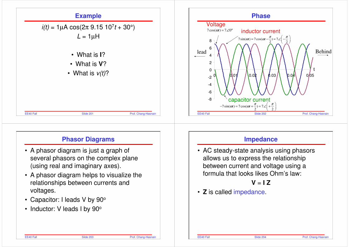
Slide 201EE40 Fall2006
Prof. Chang-Hasnain
Example
i(t) = 1µA cos(2π 9.15 107t + 30°)
L = 1µH
• What is I?
• What is V?
• What is v(t)?
Slide 202EE40 Fall2006
Prof. Chang-Hasnain
-8
-6
-4
2
4
6
8
-2
0
0 0.01 0.02 0.03 0.04 0.05
Phase
7sin( ) 7 cos( ) 72 2
t tπ π
ω ω
= − = ∠ −
7 cos( ) 7 0tω = ∠ °
7sin( ) 7 cos( ) 72 2
t tπ π
ω ω
− = + = ∠ +
capacitor current
inductor current
Voltage
Behind
t
lead
Slide 203EE40 Fall2006
Prof. Chang-Hasnain
Phasor Diagrams
• A phasor diagram is just a graph of several phasors on the complex plane (using real and imaginary axes).
• A phasor diagram helps to visualize the relationships between currents and voltages.
• Capacitor: I leads V by 90o
• Inductor: V leads I by 90o
Slide 204EE40 Fall2006
Prof. Chang-Hasnain
Impedance
• AC steady-state analysis using phasorsallows us to express the relationship between current and voltage using a formula that looks likes Ohm’s law:
V = I Z
• Z is called impedance.

Slide 205EE40 Fall2006
Prof. Chang-Hasnain
Some Thoughts on Impedance
• Impedance depends on the frequency ω.
• Impedance is (often) a complex number.
• Impedance allows us to use the same solution techniques for AC steady state as we use for DC steady state.
Slide 206EE40 Fall2006
Prof. Chang-Hasnain
Example: Single Loop Circuit
20kΩ+
-1µF10V ∠ 0° VC
+
-
f=60 Hz, VC=?
How do we find VC?
First compute impedances for resistor and capacitor:
ZR = R= 20kΩ = 20kΩ ∠ 0°ZC = 1/j (2πf x 1µF) = 2.65kΩ ∠ -90°
Slide 207EE40 Fall2006
Prof. Chang-Hasnain
Impedance Example
20kΩ ∠ 0°
+
-2.65kΩ ∠ -90°10V ∠ 0° VC
+
-
Now use the voltage divider to find VC:
°∠Ω+°∠Ω
°∠Ω°∠=
0k2090-k65.2
90-k65.20 10VCV
°∠= 4.82- 1.31VCV
Slide 208EE40 Fall2006
Prof. Chang-Hasnain
What happens when ωωωω changes?
20kΩ+
-1µF10V ∠ 0° VC
+
-
ω = 10
Find VC

Slide 209EE40 Fall2006
Prof. Chang-Hasnain
Circuit Analysis Using Complex Impedances
• Suitable for AC steady state.
• KVL
• Phasor Form KCL
• Use complex impedances for inductors and capacitors and follow same analysis as in chap 2.
( ) ( ) ( )31 2
31 2
1 2 3
1 1 2 2 3 3
( )( ) ( )
1 2 3
( )( ) ( )
1 2 3
( ) ( ) ( ) 0
cos cos cos 0
Re 0
0
0
j tj t j t
jj j
v t v t v t
V t V t V t
V e V e V e
V e V e V e
ω θω θ ω θ
θθ θ
ω θ ω θ ω θ
++ +
+ + =
+ + + + + =
+ + =
+ + =
=1 2 3V + V + V
Phasor Form KVL
0=1 2 3I + I + I
Slide 210EE40 Fall2006
Prof. Chang-Hasnain
Steady-State AC Analysis
Find v(t) for ω=2π 3000
1kΩ
0.1µF5mA ∠ 0°
+
-
V
1kΩ
-j530kΩ5mA ∠ 0°
+
-
V
Slide 211EE40 Fall2006
Prof. Chang-Hasnain
Find the Equivalent Impedance
5mA ∠ 0°
+
-
VZeq
( )°−∠
°−∠×°∠=
−
−=
9.271132
90530010
5301000
5301000 3
j
jeqZ
°−∠Ω= 1.622.468eqZ
°−∠Ω×°∠== 1.622.4680mA5eqIZV
°−∠= 1.62V34.2V
)1.623000t(2cosV34.2)( °−= πtv
Slide 212EE40 Fall2006
Prof. Chang-Hasnain
Change the Frequency
Find v(t) for ω=2π 455000
1kΩ
0.1µF5mA ∠ 0°
+
-
V
1kΩ
-j3.5Ω
5mA ∠ 0°
+
-
V
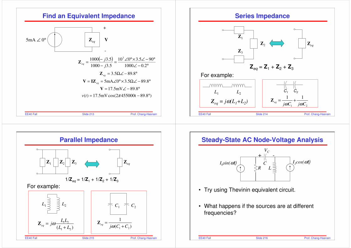
Slide 213EE40 Fall2006
Prof. Chang-Hasnain
Find an Equivalent Impedance
5mA ∠ 0°
+
-
VZeq
( )°−∠
°−∠×°∠=
−
−=
2.01000
905.3010
5.31000
5.31000 3
j
jeqZ
°−∠Ω= 8.895.3eqZ
°−∠Ω×°∠== 8.895.30mA5eqIZV
°−∠= 8.89mV5.17V
)8.89455000t(2cosmV5.17)( °−= πtv
Slide 214EE40 Fall2006
Prof. Chang-Hasnain
Series Impedance
Zeq = Z1 + Z2 + Z3
Zeq
Z1
Z3
Z2
L2L1
Zeq = jω(L1+L2)
For example:
1 2
1 1eq
j C j Cω ω= +Z
C1 C2
Slide 215EE40 Fall2006
Prof. Chang-Hasnain
Parallel Impedance
1/Zeq = 1/Z1 + 1/Z2 + 1/Z3
Z3Z1 Z2 Zeq
C1 C2
1 2
1
( )eq
j C Cω=
+Z
For example:
L2L1
1 2
1 2( )
eq
L Lj
L Lω=
+Z
Slide 216EE40 Fall2006
Prof. Chang-Hasnain
Steady-State AC Node-Voltage Analysis
CI0sin(ωt) I1cos(ωt)
R L
• Try using Thevinin equivalent circuit.
• What happens if the sources are at different
frequencies?
+ -VC
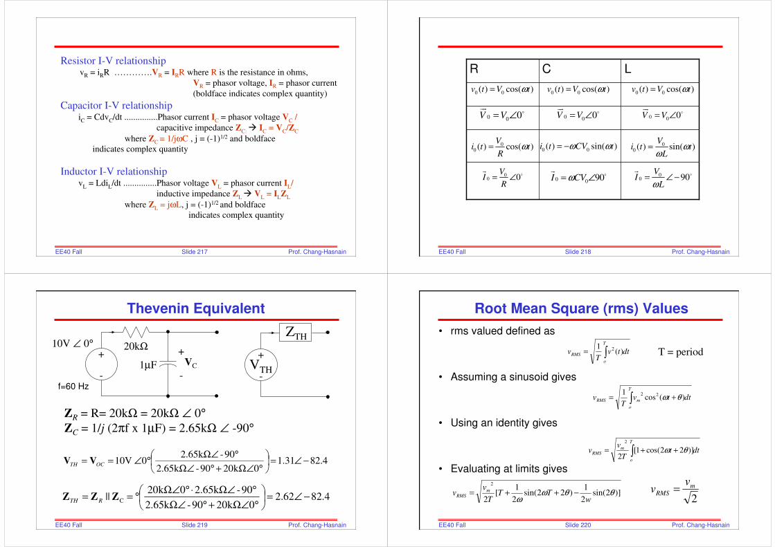
Slide 217EE40 Fall2006
Prof. Chang-Hasnain
Resistor I-V relationshipvR = iRR ………….VR = IRR where R is the resistance in ohms,
VR = phasor voltage, IR = phasor current
(boldface indicates complex quantity)
Capacitor I-V relationshipiC
= CdvC/dt ...............Phasor current I
C= phasor voltage V
C/
capacitive impedance ZC: I
C= V
C/Z
C
where ZC
= 1/jωC , j = (-1)1/2 and boldface
indicates complex quantity
Inductor I-V relationshipv
L= Ldi
L/dt ...............Phasor voltage V
L= phasor current I
L/
inductive impedance ZL V
L= I
LZ
L
where ZL
= jωL, j = (-1)1/2 and boldface
indicates complex quantity
Slide 218EE40 Fall2006
Prof. Chang-Hasnain
0 0( ) cos( )v t V tω=
00 0
VI
R= ∠
0 0 0V V= ∠
0 0 90I CVω= ∠
0
0 90V
ILω
= ∠ −
0 0( ) cos( )v t V tω=
00 ( ) sin( )
Vi t t
Lω
ω=0 0
( ) sin( )i t CV tω ω= −00 ( ) cos( )
Vi t t
Rω=
0 0( ) cos( )v t V tω=
0 0 0V V= ∠
0 0 0V V= ∠
LCR
Slide 219EE40 Fall2006
Prof. Chang-Hasnain
Thevenin Equivalent
f=60 Hz
4.8231.10k2090-k65.2
90-k65.20 10V −∠=
°∠Ω+°∠Ω
°∠Ω°∠== OCTH VV
20kΩ+
-1µF
10V ∠ 0°
VC
+
-
ZR = R= 20kΩ = 20kΩ ∠ 0°ZC = 1/j (2πf x 1µF) = 2.65kΩ ∠ -90°
+
-
ZTH
VTH
4.8262.20k2090-k65.2
90-k65.20k20 || C −∠=
°∠Ω+°∠Ω
°∠Ω⋅°∠Ω°== ZZZ RTH
Slide 220EE40 Fall2006
Prof. Chang-Hasnain
Root Mean Square (rms) Values
• rms valued defined as
• Assuming a sinusoid gives
• Using an identity gives
• Evaluating at limits gives
dttvT
v
T
o
RMS ∫= )(1 2
dttvT
v
T
o
mRMS ∫ += )(cos1 22
θω
dttT
vv
T
o
mRMS ∫ ++= )]22cos(1[
2
2
θω
)]2sin(2
1)22sin(
2
1[
2
2
θθωω w
TTT
vv m
RMS −++=2
mRMS
vv =
T = period
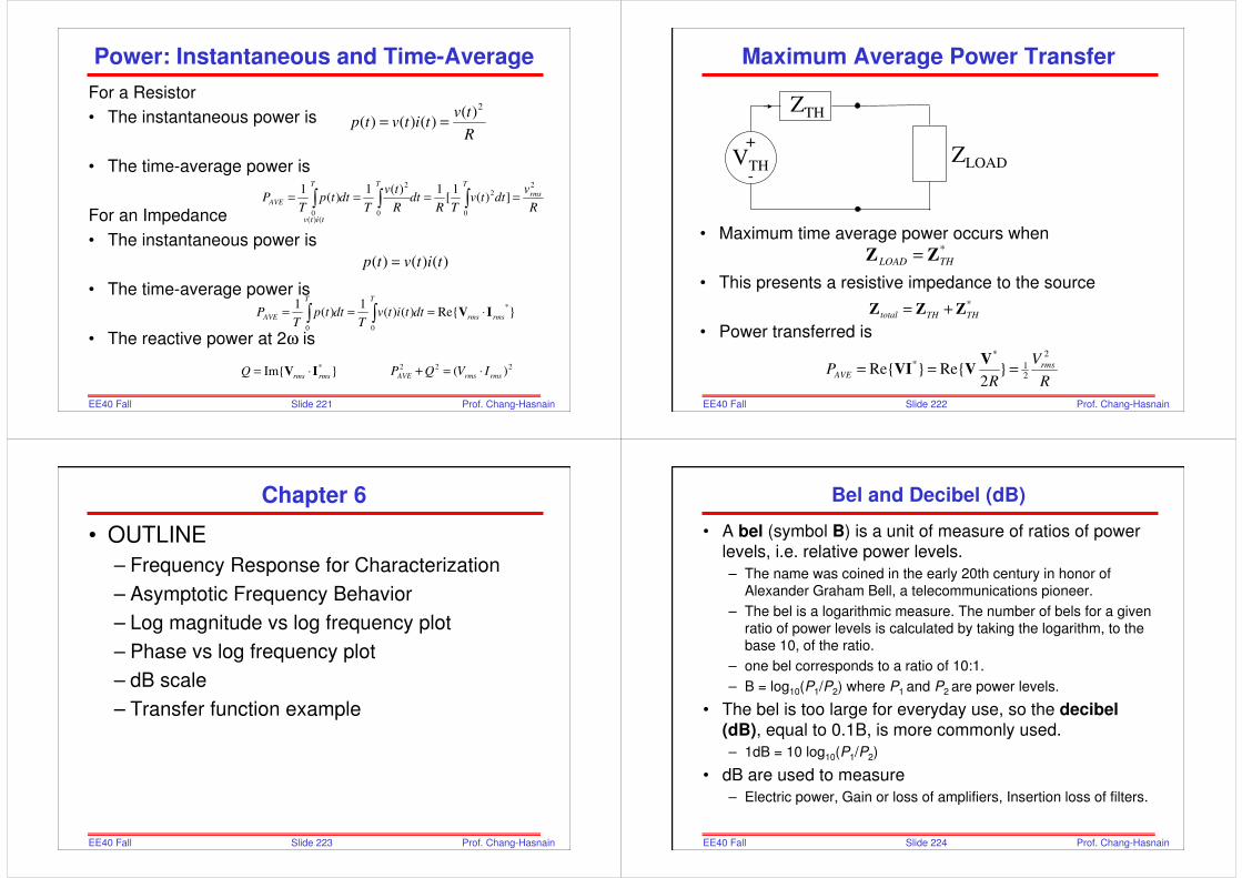
Slide 221EE40 Fall2006
Prof. Chang-Hasnain
Power: Instantaneous and Time-Average
For a Resistor
• The instantaneous power is
• The time-average power is
For an Impedance
• The instantaneous power is
• The time-average power is
• The reactive power at 2ω is
R
tvtitvtp
2)()()()( ==
R
vdttv
TRdt
R
tv
Tdttp
TP rms
TTT
AVE
2
0
2
0
2
0
])(1
[1)(1
)(1
==== ∫∫∫
)()()( titvtp =
Re)()(1
)(1 *
00
rmsrms
TT
AVE dttitvT
dttpT
P IV ⋅=== ∫∫
titv ()(
Im *
rmsrmsQ IV ⋅= 222 )( rmsrmsAVE IVQP ⋅=+
Slide 222EE40 Fall2006
Prof. Chang-Hasnain
Maximum Average Power Transfer
• Maximum time average power occurs when
• This presents a resistive impedance to the source
• Power transferred is
*
THLOAD ZZ =
+
-
ZTH
VTHZLOAD
*
THTHtotal ZZZ +=
R
V
RP rms
AVE
2
21
**
2ReRe ===
VVVI
Slide 223EE40 Fall2006
Prof. Chang-Hasnain
Chapter 6
• OUTLINE
– Frequency Response for Characterization
– Asymptotic Frequency Behavior
– Log magnitude vs log frequency plot
– Phase vs log frequency plot
– dB scale
– Transfer function example
Slide 224EE40 Fall2006
Prof. Chang-Hasnain
Bel and Decibel (dB)
• A bel (symbol B) is a unit of measure of ratios of powerlevels, i.e. relative power levels.
– The name was coined in the early 20th century in honor of Alexander Graham Bell, a telecommunications pioneer.
– The bel is a logarithmic measure. The number of bels for a given ratio of power levels is calculated by taking the logarithm, to the base 10, of the ratio.
– one bel corresponds to a ratio of 10:1.
– B = log10(P1/P2) where P1 and P2 are power levels.
• The bel is too large for everyday use, so the decibel (dB), equal to 0.1B, is more commonly used.
– 1dB = 10 log10(P1/P2)
• dB are used to measure
– Electric power, Gain or loss of amplifiers, Insertion loss of filters.
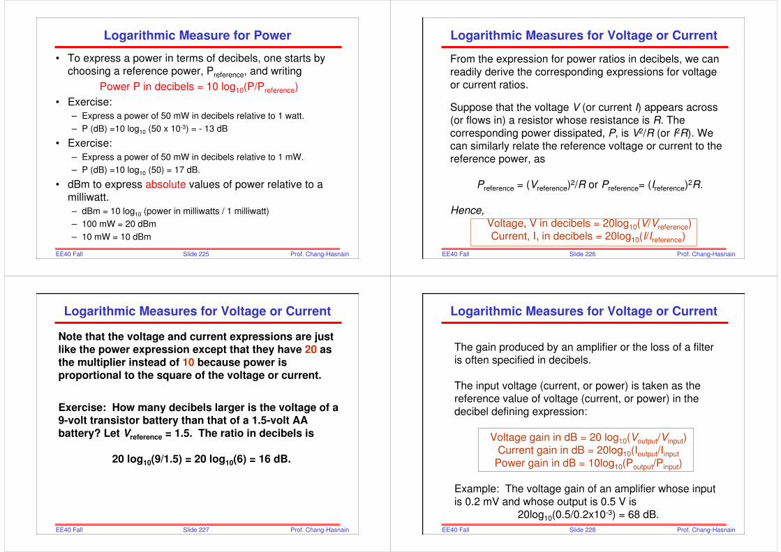
Slide 225EE40 Fall2006
Prof. Chang-Hasnain
Logarithmic Measure for Power
• To express a power in terms of decibels, one starts by choosing a reference power, Preference, and writing
Power P in decibels = 10 log10(P/Preference)
• Exercise:
– Express a power of 50 mW in decibels relative to 1 watt.
– P (dB) =10 log10 (50 x 10-3) = - 13 dB
• Exercise:
– Express a power of 50 mW in decibels relative to 1 mW.
– P (dB) =10 log10 (50) = 17 dB.
• dBm to express absolute values of power relative to a milliwatt.
– dBm = 10 log10 (power in milliwatts / 1 milliwatt)
– 100 mW = 20 dBm
– 10 mW = 10 dBm
Slide 226EE40 Fall2006
Prof. Chang-Hasnain
From the expression for power ratios in decibels, we can
readily derive the corresponding expressions for voltage
or current ratios.
Suppose that the voltage V (or current I) appears across
(or flows in) a resistor whose resistance is R. The
corresponding power dissipated, P, is V2/R (or I2R). We can similarly relate the reference voltage or current to the
reference power, as
Preference = (Vreference)2/R or Preference= (Ireference)
2R.
Hence,
Voltage, V in decibels = 20log10(V/Vreference)Current, I, in decibels = 20log10(I/Ireference)
Logarithmic Measures for Voltage or Current
Slide 227EE40 Fall2006
Prof. Chang-Hasnain
Note that the voltage and current expressions are just like the power expression except that they have 20 as the multiplier instead of 10 because power is proportional to the square of the voltage or current.
Exercise: How many decibels larger is the voltage of a 9-volt transistor battery than that of a 1.5-volt AA battery? Let Vreference = 1.5. The ratio in decibels is
20 log10(9/1.5) = 20 log10(6) = 16 dB.
Logarithmic Measures for Voltage or Current
Slide 228EE40 Fall2006
Prof. Chang-Hasnain
The gain produced by an amplifier or the loss of a filter is often specified in decibels.
The input voltage (current, or power) is taken as the
reference value of voltage (current, or power) in the
decibel defining expression:
Voltage gain in dB = 20 log10(Voutput/Vinput)Current gain in dB = 20log10(Ioutput/Iinput
Power gain in dB = 10log10(Poutput/Pinput)
Example: The voltage gain of an amplifier whose input
is 0.2 mV and whose output is 0.5 V is 20log10(0.5/0.2x10-3) = 68 dB.
Logarithmic Measures for Voltage or Current

Slide 229EE40 Fall2006
Prof. Chang-Hasnain
Bode Plot
• Plot of magnitude of transfer function vs. frequency
– Both x and y scale are in log scale
– Y scale in dB
• Log Frequency Scale
– Decade Ratio of higher to lower frequency
= 10
– Octave Ratio of higher to lower frequency
= 2
Slide 230EE40 Fall2006
Prof. Chang-Hasnain
Frequency Response
• The shape of the frequency response of the complex
ratio of phasors VOUT/VIN is a convenient means of classifying a circuit behavior and identifying key
parameters.
Frequency
Low Pass
IN
OUT
V
V
GainBreak point
IN
OUT
V
V
Frequency
High Pass
Gain
Break point
FYI: These are log ratio vs log frequency plots
Slide 231EE40 Fall2006
Prof. Chang-Hasnain
Example Circuit
)1()/1
)/1(
22 CRj
A
CjR
jwCA
IN
OUT
ωω +=
+=
V
V
IN
OUTnctionTransferFuV
V=
−
+
AVT
R2
R1
+
VT
+
VOUT
CVIN
+
cR
c
IN
OUT
ZZ
AZ
+=
V
V
A = 100
R1 = 100,000 Ohms
R2 = 1000 Ohms
C = 10 uF
Slide 232EE40 Fall2006
Prof. Chang-Hasnain
Break Point Values
• When dealing with resonant circuits it is convenient to refer to the frequency difference between points at which the power from the circuit is half that at the peak of resonance.
• Such frequencies are known as “half-power frequencies”, and the power output there referred to the peak power (at the resonant frequency) is
• 10log10(Phalf-power/Presonance) = 10log10(1/2) = -3 dB.
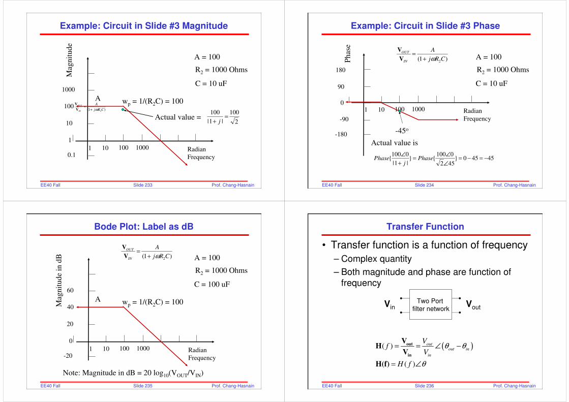
Slide 233EE40 Fall2006
Prof. Chang-Hasnain
Example: Circuit in Slide #3 Magnitude
)1( 2CRj
A
IN
OUT
ω+=
V
V
1
10
100
1000
0.110 100 10001 Radian
Frequency
A = 100
R2 = 1000 Ohms
C = 10 uF
wp = 1/(R2C) = 100A
Mag
nit
ud
e
Actual value = 2
100
|1|
100=
+ j
Slide 234EE40 Fall2006
Prof. Chang-Hasnain
Example: Circuit in Slide #3 Phase
)1( 2CRj
A
IN
OUT
ω+=
V
V
-90
0
90
180
-180
10 100 10001 Radian
Frequency
-45o
A = 100
R2 = 1000 Ohms
C = 10 uF
Ph
ase
Actual value is
45450452
0100
|1|
0100 −=−=
∠
∠=
+
∠Phase
jPhase
Slide 235EE40 Fall2006
Prof. Chang-Hasnain
Bode Plot: Label as dB
0
20
40
60
-2010 100 10001 Radian
Frequency
)1( 2CRj
A
IN
OUT
ω+=
V
V
A = 100
R2 = 1000 Ohms
C = 100 uF
wp = 1/(R2C) = 100A
Mag
nit
ud
e in
dB
Note: Magnitude in dB = 20 log10(VOUT/VIN)
Slide 236EE40 Fall2006
Prof. Chang-Hasnain
Transfer Function
• Transfer function is a function of frequency
– Complex quantity
– Both magnitude and phase are function of
frequency
Two Port filter network
Vin Vout
( )( )
( )
outout in
in
Vf
V
H f
θ θ
θ
= = ∠ −
= ∠
out
in
VH
V
H(f)
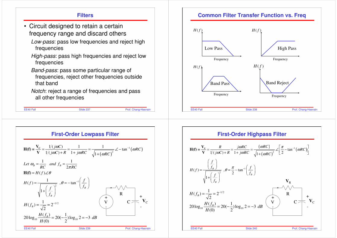
Slide 237EE40 Fall2006
Prof. Chang-Hasnain
Filters
• Circuit designed to retain a certain frequency range and discard others
Low-pass: pass low frequencies and reject high
frequencies
High-pass: pass high frequencies and reject low
frequencies
Band-pass: pass some particular range of
frequencies, reject other frequencies outside
that band
Notch: reject a range of frequencies and pass
all other frequencies
Slide 238EE40 Fall2006
Prof. Chang-Hasnain
Common Filter Transfer Function vs. Freq
( )H f
Frequency
High Pass
( )H f
Frequency
Low Pass
( )H f
Frequency
Band Pass
Frequency
Band Reject
( )H f
Slide 239EE40 Fall2006
Prof. Chang-Hasnain
First-Order Lowpass Filter
( )( )1
2
1
2
1 ( ) 1 1tan
1 ( ) 1 1
1 1
2
( )
1( ) , tan
1
B B
B
B
j CRC
j C R j RC RC
Let and fRC RC
H f
fH f
ff
f
ωω
ω ω ω
ωπ
θ
θ
−
−
= = = ∠ −+ + +
= =
= ∠
= = −
+
CVH(f) =
V
H(f)
R+
-CV VC
+
-1/ 2
10 10
1( ) 2
2
( ) 120log 20( ) log 2 3
(0) 2
B
B
H f
H fdB
H
−= =
= − = −
Slide 240EE40 Fall2006
Prof. Chang-Hasnain
First-Order Highpass Filter
( )
( )( )1
2
1
2
tan1 ( ) 1 21
( ) , tan2
1
R
B
B
B
RCR j RCRC
j C R j RC RC
f
f fH f
ff
f
ωω πω
ω ω ω
πθ
−
−
= = = ∠ − + + +
= = −
+
VH(f) =
V
R+
-CV VC
+
-
1/ 2
10 10
1( ) 2
2
( ) 120log 20( ) log 2 3
(0) 2
B
B
H f
H fdB
H
−= =
= − = −
VR
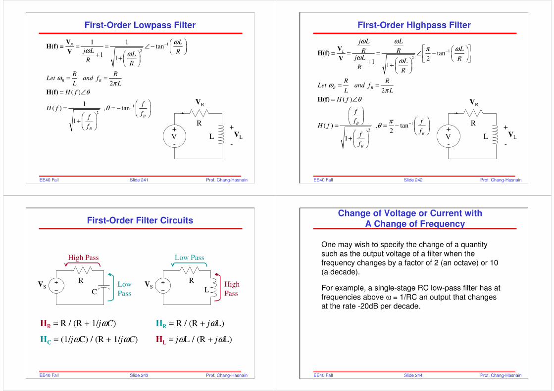
Slide 241EE40 Fall2006
Prof. Chang-Hasnain
First-Order Lowpass Filter
1
2
1
2
1 1tan
11
2
( )
1( ) , tan
1
R
B B
B
B
L
j L RLR
R
R RLet and f
L L
H f
fH f
ff
f
ωω ω
ωπ
θ
θ
−
−
= = ∠ −
++
= =
= ∠
= = −
+
VH(f) =
V
H(f)
R+
-LV VL
+
-
VR
Slide 242EE40 Fall2006
Prof. Chang-Hasnain
First-Order Highpass Filter
1
2
1
2
tan2
11
2
( )
( ) , tan2
1
L
B B
B
B
B
j L L
LR Rj L RLR
R
R RLet and f
L L
H f
f
f fH f
ff
f
ω ωπ ω
ω ω
ωπ
θ
πθ
−
−
= = ∠ −
++
= =
= ∠
= = −
+
VH(f) =
V
H(f)
R+
-LV VL
+
-
VR
Slide 243EE40 Fall2006
Prof. Chang-Hasnain
First-Order Filter Circuits
L+
–VS
C
R
Low Pass
High
Pass
HR = R / (R + jωL)
HL = jωL / (R + jωL)
+
–VS
R
High Pass
Low
Pass
HR = R / (R + 1/jωC)
HC = (1/jωC) / (R + 1/jωC)
Slide 244EE40 Fall2006
Prof. Chang-Hasnain
Change of Voltage or Current withA Change of Frequency
One may wish to specify the change of a quantity
such as the output voltage of a filter when the frequency changes by a factor of 2 (an octave) or 10
(a decade).
For example, a single-stage RC low-pass filter has at
frequencies above ω = 1/RC an output that changes at the rate -20dB per decade.
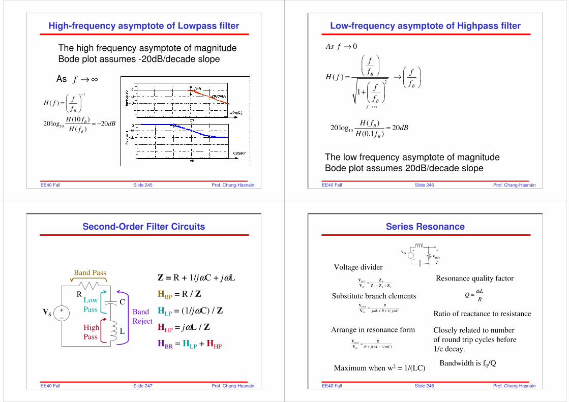
Slide 245EE40 Fall2006
Prof. Chang-Hasnain
High-frequency asymptote of Lowpass filter
1
10
( )
(10 )20log 20
( )
B
B
B
fH f
f
H fdB
H f
−
=
= −
As f → ∞
The high frequency asymptote of magnitude
Bode plot assumes -20dB/decade slope
Slide 246EE40 Fall2006
Prof. Chang-Hasnain
Low-frequency asymptote of Highpass filter
f → ∞
10
( )20 log 20
(0.1 )
B
B
H fdB
H f=
The low frequency asymptote of magnitude
Bode plot assumes 20dB/decade slope
2
0
( )
1
B
B
B
As f
f
f fH f
ff
f
→
= →
+
Slide 247EE40 Fall2006
Prof. Chang-Hasnain
Second-Order Filter Circuits
C+
–VS
R
Band Pass
Low
Pass
LHigh
Pass
Band
Reject
Z = R + 1/jωC + jωL
HBP = R / Z
HLP = (1/jωC) / Z
HHP = jωL / Z
HBR = HLP + HHP
Slide 248EE40 Fall2006
Prof. Chang-Hasnain
Series Resonance
CRL
R
IN
OUT
ZZZ
Z
V
V
++=
CjRLj
R
IN
OUT
ωω /1++=
V
V
)/1( CLjR
R
IN
OUT
ωω −+=
V
V
+
−
VIN
VOUT
+
Voltage divider
Substitute branch elements
Arrange in resonance form
Maximum when w2 = 1/(LC)
Resonance quality factor
R
LQ
ω=
Ratio of reactance to resistance
Closely related to number
of round trip cycles before
1/e decay.
Bandwidth is f0/Q

Slide 249EE40 Fall2006
Prof. Chang-Hasnain
Parallel Resonance
CRL
SOUT
YYY
IV
++=
jwCRLj
SOUT
++=
11ω
IV
IIN
VOUT
+
)1(1L
CjR
SOUT
ωω −+
=I
V
Admittance
Substitute branch elements
Arrange in resonance form
Maximum = IS/R when w2 = 1/(LC)
Resonance quality factor
R
LQ
ω=
Ratio of reactance to resistance
Closely related to number
of round trip cycles before
1/e decay.
Bandwidth is f0/Q
Slide 250EE40 Fall2006
Prof. Chang-Hasnain
Chapter 14
• OUTLINE
– Op-Amp from 2-Port Blocks
– Op-Amp Model and its Idealization
– Negative Feedback for Stability
– Components around Op-Amp define the
Circuit Function
• Reading
– Chap 14
Slide 251EE40 Fall2006
Prof. Chang-Hasnain
The Operational Amplifier
• The operational amplifier (“op amp”) is a basic building block used in analog circuits.
– Its behavior is modeled using a dependent source.
– When combined with resistors, capacitors, and inductors, it can perform various useful functions:
• amplification/scaling of an input signal• sign changing (inversion) of an input signal
• addition of multiple input signals
• subtraction of one input signal from another
• integration (over time) of an input signal
• differentiation (with respect to time) of an input signal• analog filtering• nonlinear functions like exponential, log, sqrt, etc
– Isolate input from output; allow cascading
Slide 252EE40 Fall2006
Prof. Chang-Hasnain
High Quality Dependent Source In an Amplifier
V0 depends only on input (V+ − V-)
)VV(AV0 −+ −=
+
−A
V+
V−
V0
Differential Amplifier
AMPLIFIER SYMBOL
+
−
+
−V0AV1
+
−V1
Ri
Circuit Model in linear region
AMPLIFIER MODEL
See the utility of this: this Model when used correctly
mimics the behavior of an amplifier but omits the
complication of the many many transistors and other
components.
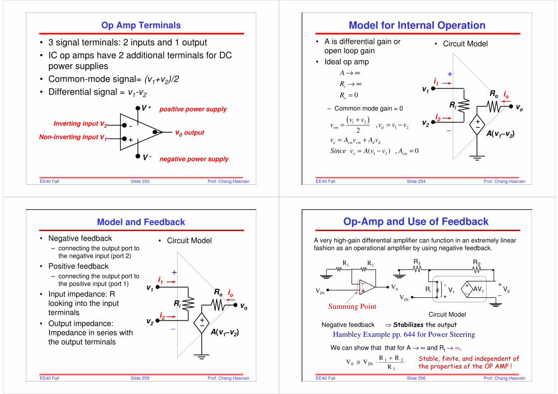
Slide 253EE40 Fall2006
Prof. Chang-Hasnain
Op Amp Terminals
• 3 signal terminals: 2 inputs and 1 output
• IC op amps have 2 additional terminals for DC
power supplies
• Common-mode signal= (v1+v2)/2
• Differential signal = v1-v2
-
+
V +
V –
Inverting input v2
Non-inverting input v1
positive power supply
negative power supply
v0 output
Slide 254EE40 Fall2006
Prof. Chang-Hasnain
Model for Internal Operation
• A is differential gain or open loop gain
• Ideal op amp
– Common mode gain = 0
0
i
o
A
R
R
→ ∞
→ ∞
=v1
v2
Ri
+–
Ro
vo
A(v1–v2)
i1
i2
io
+
_
• Circuit Model
( )1 2
1 2
1 2
,2
( ) , 0
cm d
o cm cm d d
o cm
v vv v v v
v A v A v
Since v A v v A
+= = −
= +
= − =
Slide 255EE40 Fall2006
Prof. Chang-Hasnain
Model and Feedback
• Negative feedback
– connecting the output port to the negative input (port 2)
• Positive feedback
– connecting the output port to the positive input (port 1)
• Input impedance: R
looking into the input terminals
• Output impedance: Impedance in series with
the output terminals
v1
v2
Ri
+–
Ro
vo
A(v1–v2)
i1
i2
io
+
_
• Circuit Model
Slide 256EE40 Fall2006
Prof. Chang-Hasnain
Op-Amp and Use of Feedback
A very high-gain differential amplifier can function in an extremely linear fashion as an operational amplifier by using negative feedback.
Negative feedback ⇒ Stabilizes the output
R2R1
−+
V0VIN
We can show that that for A → ∞ and Ri → ∞,
1
21IN0
R
RRVV
+⋅≅
+
−
+
−V0AV1
-
+V1
Ri
R2
Circuit Model
R1
VIN
Stable, finite, and independent of the properties of the OP AMP !
Hambley Example pp. 644 for Power Steering
Summing Point
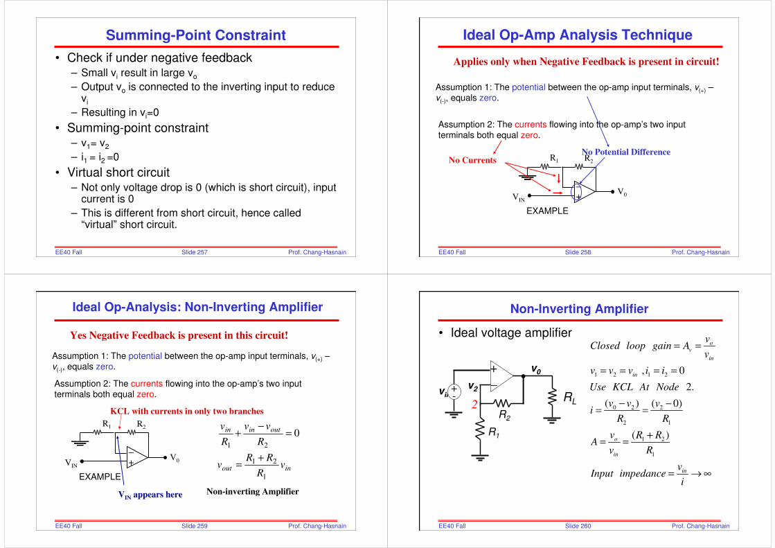
Slide 257EE40 Fall2006
Prof. Chang-Hasnain
Summing-Point Constraint
• Check if under negative feedback– Small vi result in large vo
– Output vo is connected to the inverting input to reduce vi
– Resulting in vi=0
• Summing-point constraint– v1= v2
– i1 = i2 =0
• Virtual short circuit– Not only voltage drop is 0 (which is short circuit), input
current is 0
– This is different from short circuit, hence called “virtual” short circuit.
Slide 258EE40 Fall2006
Prof. Chang-Hasnain
Ideal Op-Amp Analysis Technique
Assumption 1: The potential between the op-amp input terminals, v(+) –v(-), equals zero.
R2R1
−+
V0VIN
EXAMPLE
Assumption 2: The currents flowing into the op-amp’s two input terminals both equal zero.
No Potential DifferenceNo Currents
Applies only when Negative Feedback is present in circuit!
Slide 259EE40 Fall2006
Prof. Chang-Hasnain
Ideal Op-Analysis: Non-Inverting Amplifier
Assumption 1: The potential between the op-amp input terminals, v(+) –v(-), equals zero.
R2R1
−+
V0VIN
EXAMPLE
Assumption 2: The currents flowing into the op-amp’s two input terminals both equal zero.
021
=−
+R
vv
R
v outinin
inout vR
RRv
1
21 +=
KCL with currents in only two branches
Non-inverting AmplifierVIN appears here
Yes Negative Feedback is present in this circuit!
Slide 260EE40 Fall2006
Prof. Chang-Hasnain
Non-Inverting Amplifier
• Ideal voltage amplifier
_
+
vin+-
R2
R1
RL
v2
v0 1 2 1 2
0 2 2
2 1
1 2
1
, 0
2.
( ) ( 0)
( )
ov
in
in
o
in
in
vClosed loop gain A
v
v v v i i
Use KCL At Node
v v vi
R R
v R RA
v R
vInput impedance
i
= =
= = = =
− −= =
+= =
= → ∞
2
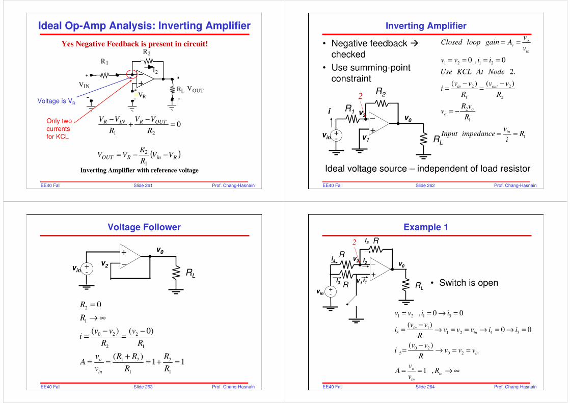
Slide 261EE40 Fall2006
Prof. Chang-Hasnain
Ideal Op-Amp Analysis: Inverting Amplifier
R2
I2
VOUT-VR
R1
RLVIN
021
=−
+−
R
VV
R
VV OUTRINR
( )RinROUT VVR
RVV −−=
1
2
Voltage is VR
Only two currents for KCL
Inverting Amplifier with reference voltage
Yes Negative Feedback is present in circuit!
Slide 262EE40 Fall2006
Prof. Chang-Hasnain
Inverting Amplifier
• Negative feedback
checked
• Use summing-point
constraint
1 2 1 2
2 2
1 2
2
1
1
0 , 0
2.
( ) ( )
ov
in
in out
oo
in
vClosed loop gain A
v
v v i i
Use KCL At Node
v v v vi
R R
R vv
R
vInput impedance R
i
= =
= = = =
− −= =
= −
= =
Ideal voltage source – independent of load resistor
_
+vin
+-
R2
R1
RLv1
v0
v2i
2
Slide 263EE40 Fall2006
Prof. Chang-Hasnain
Voltage Follower
_
+
vin+- RL
v2
v0
2
1
0 2 2
2 1
1 2 2
1 1
0
( ) ( 0)
( )1 1o
in
R
R
v v vi
R R
v R R RA
v R R
=
→ ∞
− −= =
+= = = + =
Slide 264EE40 Fall2006
Prof. Chang-Hasnain
Example 1
• Switch is open
1 2 1 3
13 1 2 4 5
0 25 0 2
, 0 0
( )0 0
( )
1 ,
inin
in
oin
in
v v i i
v vi v v v i i
R
v vi v v v
R
vA R
v
= = → =
−= → = = → = → =
−= → = =
= = → ∞
v1
v2
vin+-
R
RL
v0
2 R
_
+i1
i2
R
i5
i3
i4
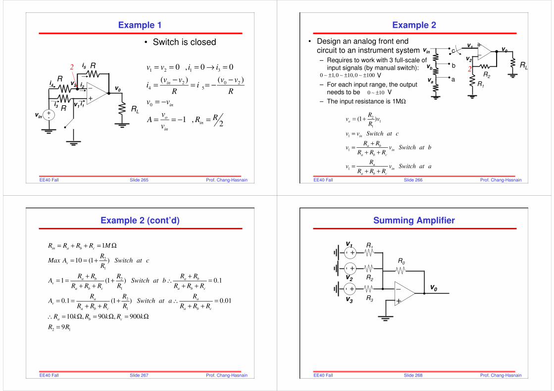
Slide 265EE40 Fall2006
Prof. Chang-Hasnain
Example 1
• Switch is closed
v1
v2
vin+-
R
RL
v0
2 R
_
+i1
i2
R
i5
i3
i4
1 2 1 3
2 0 24 5
0
0 , 0 0
( ) ( )
1 ,2
in
in
oin
in
v v i i
v v v vi i
R R
v v
v RA Rv
= = = → =
− −= = = −
= −
= = − =
Slide 266EE40 Fall2006
Prof. Chang-Hasnain
Example 2
• Design an analog front end circuit to an instrument system
– Requires to work with 3 full-scale of input signals (by manual switch):
V
– For each input range, the output needs to be V
– The input resistance is 1MΩ
0 1,0 10,0 100± ± ±∼ ∼ ∼
0 10±∼
_
+
vin
R2
R1
RL
v2
v0
2b
a
c
vb
va
v1
21
1
1
1
1
(1 )o
in
a b
in
a b c
a
in
a b c
Rv v
R
v v Switch at c
R Rv v Switch at b
R R R
Rv v Switch at a
R R R
= +
=
+=
+ +
=+ +
Slide 267EE40 Fall2006
Prof. Chang-Hasnain
Example 2 (cont’d)
2
1
2
1
2
1
2 1
1
10 (1 )
1 (1 ) 0.1
0.1 (1 ) 0.01
10 , 90 , 900
9
in a b c
v
a b a bv
a b c a b c
a av
a b c a b c
a b c
R R R R M
RMax A Switch at c
R
R R R RRA Switch at b
R R R R R R R
R RRA Switch at a
R R R R R R R
R k R k R k
R R
= + + = Ω
= = +
+ += = + ∴ =
+ + + +
= = + ∴ =+ + + +
∴ = Ω = Ω = Ω
=
Slide 268EE40 Fall2006
Prof. Chang-Hasnain
Summing Amplifier
_
+v3
+- v0
R1
R2
+-+-
R3
R0
v2
v1

Slide 269EE40 Fall2006
Prof. Chang-Hasnain
Difference Amplifier
_
+
v2
+- v0
R4
R1
+-
R3
R2
v1
Slide 270EE40 Fall2006
Prof. Chang-Hasnain
Integrator
• Want
• What is the difference
between:
o inv K v dt= ∫
R+
-C V0
+
-
vin
Slide 271EE40 Fall2006
Prof. Chang-Hasnain
Differentiator
• Want
_
+vin
+-
R
v0
C
Slide 272EE40 Fall2006
Prof. Chang-Hasnain
Bridge Amplifier
_
+
v0
vin
+-
Ra
vx
Ravx
R0
R0(1+ε)
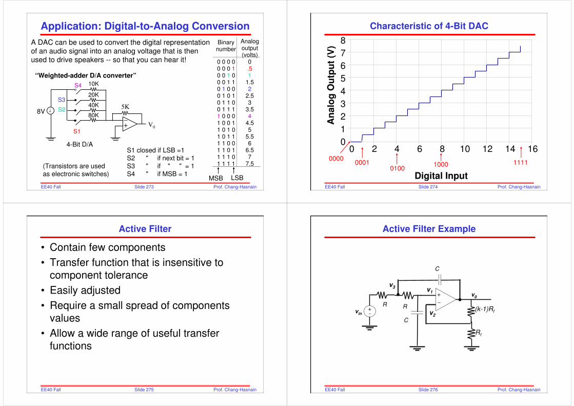
Slide 273EE40 Fall2006
Prof. Chang-Hasnain
A DAC can be used to convert the digital representation
of an audio signal into an analog voltage that is then
used to drive speakers -- so that you can hear it!
0 0 1 0 10 0 1 10 1 0 0
1.52
0 1 0 10 1 1 00 1 1 11 0 0 0
2.53
3.54
1 0 0 11 0 1 01 0 1 11 1 0 01 1 0 11 1 1 01 1 1 1
4.55
5.56
6.57
7.5
Binarynumber
Analogoutput(volts)
0 0 0 00 0 0 1
0.5
MSB LSB
S1 closed if LSB =1S2 " if next bit = 1S3 " if " " = 1S4 " if MSB = 1
4-Bit D/A
8V
−+ V0
5K
80K
40K
20K
10K
S1
+-
S3
S2
S4
−+
Application: Digital-to-Analog Conversion
“Weighted-adder D/A converter”
(Transistors are used as electronic switches)
Slide 274EE40 Fall2006
Prof. Chang-Hasnain
Digital Input
0
1
2
3
4
5
6
7
8
0 2 4 6 8 10 12 14 16
An
alo
g O
utp
ut
(V)
111110000100
00000001
Characteristic of 4-Bit DAC
Slide 275EE40 Fall2006
Prof. Chang-Hasnain
Active Filter
• Contain few components
• Transfer function that is insensitive to component tolerance
• Easily adjusted
• Require a small spread of components values
• Allow a wide range of useful transfer functions
Slide 276EE40 Fall2006
Prof. Chang-Hasnain
Active Filter Example
(k-1)Rf
Rf
_
+
R
v0
C
vin+-
R
C
v1
v2
v3

Slide 277EE40 Fall2006
Prof. Chang-Hasnain
Active Filter Solution1 2
3 11
3 3 13
2 2 2
22 2
2
2 2
2
2
( )
( ) ( )( )
1 (3 )
1 /
( )
1 (3 )
0, ( )
, ( )3
, ( )
o
ino
o
in
B
o
in
B B
B
B
B
vv v
k
v vUse KCL At Node A j Cv
R
v v v vUse KCL At Node B j C v v
R R
v k
v R C j RC k
Let RC
v kH
vk
H k DC gain
kH
k
kH
ω
ω
ω ω
ω
ωω ω
ω ω
ω ω
ω ω ω
ω ω ωω
ω
= =
−⇒ =
− −⇒ = − +
=− + −
=
= =
− + −
= =
= =−
>> = 2
20 log ( ) 40 /H decays at a rate of dB decade
ω
ω
−
∼
Slide 278EE40 Fall2006
Prof. Chang-Hasnain
Cascaded Active Filter Example
(k-1)Rf
Rf
_
+
R
v0’
C
vin
+-
R
C
v1
v2
v3
(k2 -1)Rf
Rf
_
+ v0
C2
v1’
v2’
v3’
C2
R2R2
Slide 279EE40 Fall2006
Prof. Chang-Hasnain
Cascaded Active Filter Solution
2
2 2 2 2 2 2
2 2 2 2 2
2 2 2
2
2 22 2 2 2
2 2
22 2 2 2
2 2
2
2
2
2
4
2
2
1 (3 ) 1 (3 )
1/ , 1/
( )
1 (3 ) 1 (3 )
0, ( )
, ( )3 3
, ( )
o
in
B B
o
in
B B B B
B
B
B B
v k k
v R C j R C k R C j RC k
Let RC R C
v k kH
vk k
H k k DC gain
k kH
k k
k kH
ω ω ω ω
ω ω
ωω ω ω ω
ω ω ω ω
ω ω
ω ω ω
ω ω ωω
ω ω
=− + − − + −
= =
= =
− + − − + −
= =
= =− −
>> = 4
2
20log ( ) 80 /H decays at a rate of dB decade
ω
ω
−
∼
Slide 280EE40 Fall2006
Prof. Chang-Hasnain
Chapter 10
• OUTLINE
– Diode Current and Equation
– Some Interesting Circuit Applications
– Load Line Analysis
– Solar Cells, Detectors, Zener Diodes
– Circuit Analysis with Diodes
– Half-wave Rectifier
– Clamps and Voltage Doublers using Capacitors
• Reading
– Hambley 10.1-10.8
– Supplementary Notes Chapter 2

Slide 281EE40 Fall2006
Prof. Chang-Hasnain
I-V Characteristics
In forward bias (+ on p-side) we have almost unlimited flow (very low resistance). Qualitatively, the I-V characteristics must look like:
VF
I
current increases
rapidly with V
VF
I
The current is close to zero for any negative bias
In reverse bias (+ on n-side) almost no current can flow. Qualitatively, the I-V characteristics must look like:
Slide 282EE40 Fall2006
Prof. Chang-Hasnain
Diode Physical Behavior and Equation
Ntype
Ptype
Schematic Device
+− V
I
ISymbol
+− V
Qualitative I-V characteristics:I
V
V positive, easy conduction
V negative, no conduction
Quantitative I-V characteristics:
)1e(II kTqV0 −=
In which kT/q is 0.026V and IO is a constant depending on diode area. Typical values: 10-12 to 10-16 A. Interestingly, the graph of this equation looks just like the figure to the left.
A non-ideality factor n times kT/q is often included.
Slide 283EE40 Fall2006
Prof. Chang-Hasnain
The pn Junction I vs. V Equation
In EECS 105, 130, and other courses you will learn why the I vs. V relationship for PN junctions is of the form
)1e(II kTqV0 −=
where I0 is a constant proportional to junction area and depending on doping in P and N regions, k is Boltzman constant, and T is absolute temperature.
a typical value for I0 is
,106.1hargec electronicq 19−×==
,Kat300 0.026VqKT °= A1010 1512 −− −
We note that in forward bias, I increases exponentially and is in
the µA-mA range for voltages typically in the range of 0.6-0.8V. In reverse bias, the current is essentially zero.
I-V characteristic of PN junctions
Slide 284EE40 Fall2006
Prof. Chang-Hasnain
Diode Ideal (Perfect Rectifier) Model
The equation
is graphed below for
1)kT
qVexp(II 0 −=
A10I 15
0
−=
The characteristic is described as a “rectifier” – that is, a device that permits current to pass in only one direction. (The hydraulic analog is a “check value”.) Hence the symbol:
+− V
I
Simple “Perfect Rectifier” Model
If we can ignore the small forward-bias voltage drop of a diode, a simple effective model is the “perfect rectifier,” whose I-V characteristic is given below:
V
I
Reverse bias0Vany ,0I <≅
Forward bias0Iany ,0V >≅
A perfect rectifier
0
2
4
6
8
10
-5 0 5 10
Current
in mA
Forward
Voltage in V
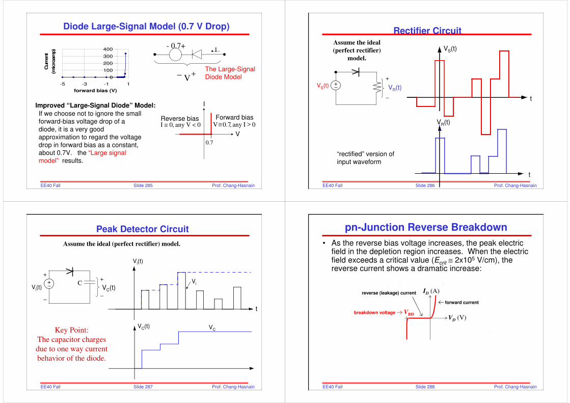
Slide 285EE40 Fall2006
Prof. Chang-Hasnain
Diode Large-Signal Model (0.7 V Drop)
Improved “Large-Signal Diode” Model:
If we choose not to ignore the small forward-bias voltage drop of a diode, it is a very good approximation to regard the voltage drop in forward bias as a constant, about 0.7V. the “Large signal model” results.
Reverse bias0Vany ,0I <≅
Forward bias0Iany ,0.7V >≅
0
100
200
300
400
-5 -3 -1 1
forward bias (V)
Curr
ent
(mic
roam
p)
+− V
I
The Large-Signal Diode Model
- 0.7+
V
I
0.7
Slide 286EE40 Fall2006
Prof. Chang-Hasnain
Rectifier Circuit
VS(t)
t
+
−
VR(t)+−VS(t)
VR(t)
“rectified” version of input waveform
t
Assume the ideal
(perfect rectifier)
model.
Slide 287EE40 Fall2006
Prof. Chang-Hasnain
Peak Detector Circuit
+
−
VC(t)Vi(t)
+
−
C
Vi(t)
Vi
t
VC(t) VC
+−
Assume the ideal (perfect rectifier) model.
Key Point:
The capacitor charges
due to one way current
behavior of the diode.
Slide 288EE40 Fall2006
Prof. Chang-Hasnain
pn-Junction Reverse Breakdown
• As the reverse bias voltage increases, the peak electric field in the depletion region increases. When the electric field exceeds a critical value (Ecrit ≅ 2x10⁵ V/cm), the reverse current shows a dramatic increase:
ID (A)
VD (V)
reverse (leakage) current
forward current
breakdown voltage VBD
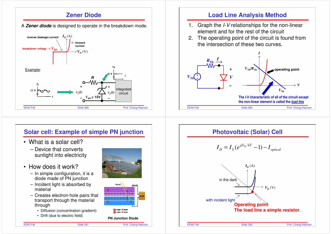
Slide 289EE40 Fall2006
Prof. Chang-Hasnain
integrated
circuit
A Zener diode is designed to operate in the breakdown mode.
Zener Diode
ID (A)
VD (V)
reverse (leakage) current
forward current
breakdown voltage
R
VBD = 15V
VBD
+
vs(t)
–
t
+
vo(t)
–
Example:
Slide 290EE40 Fall2006
Prof. Chang-Hasnain
Load Line Analysis Method
1. Graph the I-V relationships for the non-linear
element and for the rest of the circuit
2. The operating point of the circuit is found from
the intersection of these two curves.
VTh+−−−−
+
V
–
RThI
I
V
The I-V characteristic of all of the circuit except
the non-linear element is called the load line
VTh
VTh/RTh operating point
Slide 291EE40 Fall2006
Prof. Chang-Hasnain
Solar cell: Example of simple PN junction
• What is a solar cell?– Device that converts
sunlight into electricity
• How does it work?– In simple configuration, it is a
diode made of PN junction
– Incident light is absorbed by material
– Creates electron-hole pairs that transport through the material through
• Diffusion (concentration gradient)
• Drift (due to electric field)PN Junction Diode
Slide 292EE40 Fall2006
Prof. Chang-Hasnain
optical
kTVq
SD IeII −−= )1( D
Photovoltaic (Solar) Cell
ID (A)
VD (V)
with incident light
in the dark
Operating pointThe load line a simple resistor.
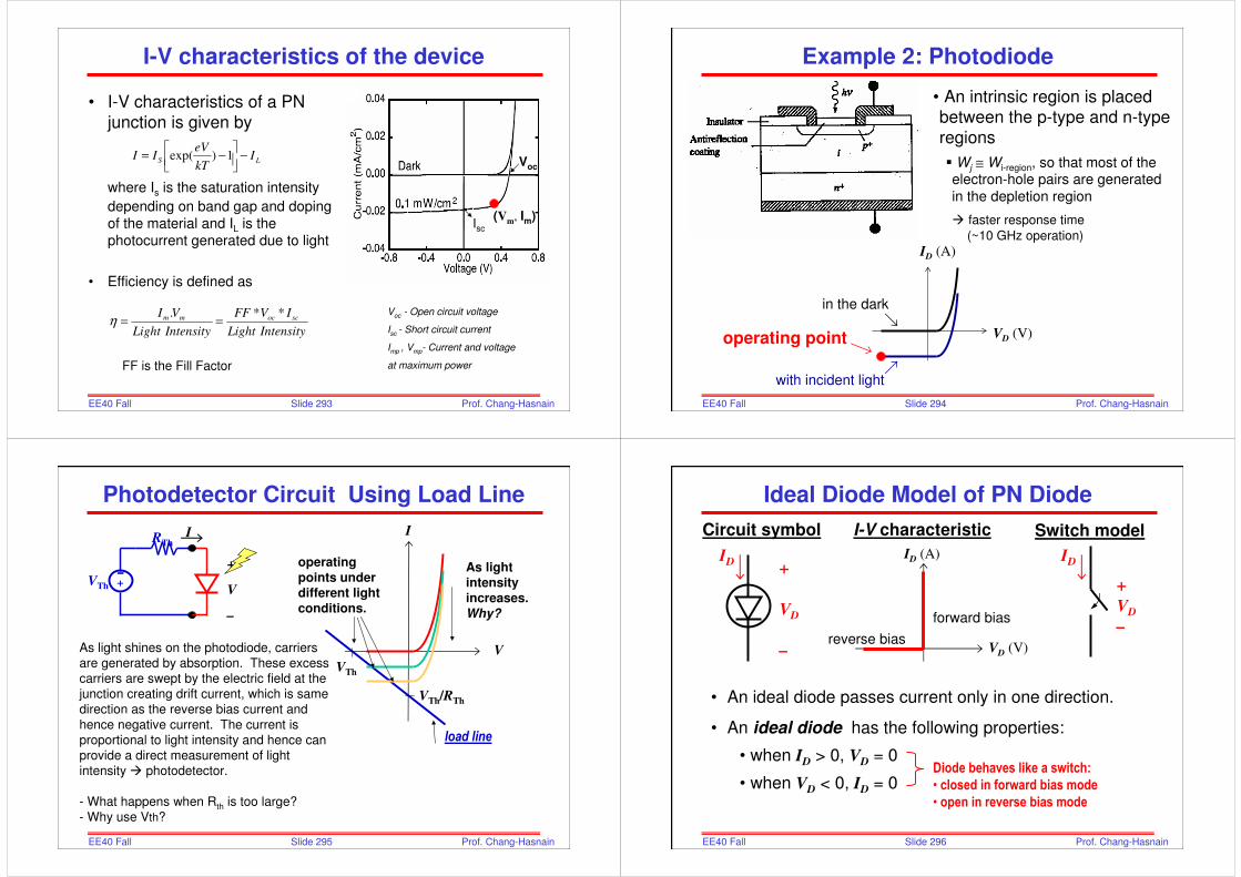
Slide 293EE40 Fall2006
Prof. Chang-Hasnain
I-V characteristics of the device
• I-V characteristics of a PN
junction is given by
where Is is the saturation intensity
depending on band gap and doping of the material and IL is the photocurrent generated due to light
• Efficiency is defined as
Voc
Isc
(Vm, Im)
LS IkT
eVII −
−= 1)exp(
IntensityLight
IVFF
IntensityLight
VI scocmm **.==η
Voc - Open circuit voltage
Isc - Short circuit current
Imp , Vmp- Current and voltage
at maximum powerFF is the Fill Factor
Slide 294EE40 Fall2006
Prof. Chang-Hasnain
Example 2: Photodiode
• An intrinsic region is placed between the p-type and n-type
regions
Wj ≅ Wi-region, so that most of the electron-hole pairs are generated in the depletion region
faster response time
(~10 GHz operation)
ID (A)
VD (V)
with incident light
in the dark
operating point
Slide 295EE40 Fall2006
Prof. Chang-Hasnain
Photodetector Circuit Using Load Line
I
V
load line
VTh
VTh/RTh
operating points under different light conditions.
As light shines on the photodiode, carriers
are generated by absorption. These excess
carriers are swept by the electric field at the
junction creating drift current, which is same
direction as the reverse bias current and
hence negative current. The current is
proportional to light intensity and hence can
provide a direct measurement of light
intensity photodetector.
- What happens when Rth is too large?
- Why use Vth?
VTh
+−−−− +
V
–
RThI
As light intensity increases. Why?
Slide 296EE40 Fall2006
Prof. Chang-Hasnain
reverse bias
forward bias
• An ideal diode passes current only in one direction.
• An ideal diode has the following properties:
• when ID > 0, VD = 0
• when VD < 0, ID = 0
Ideal Diode Model of PN Diode
ID (A)
VD (V)
ID+
VD
–
+
VD
–
ID
Circuit symbol I-V characteristic
Diode behaves like a switch:
• closed in forward bias mode
• open in reverse bias mode
Switch model
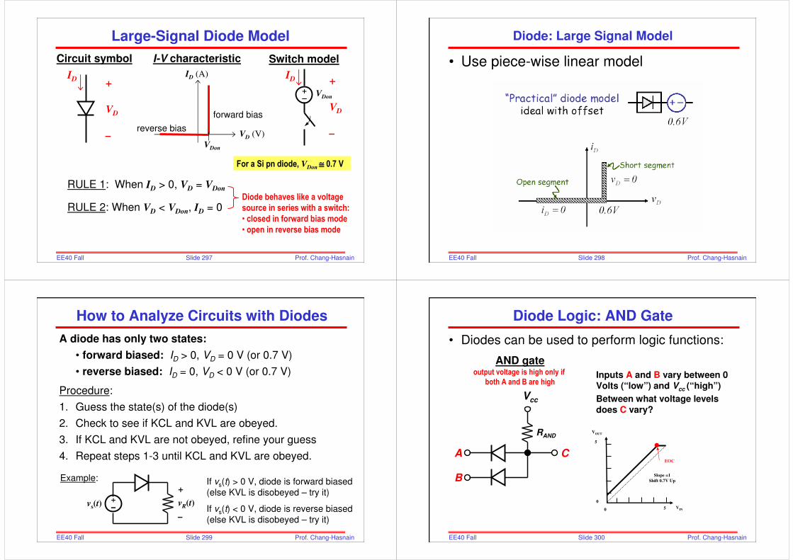
Slide 297EE40 Fall2006
Prof. Chang-Hasnain
Large-Signal Diode Model
reverse bias
forward bias
ID (A)
VD (V)
ID+
VD
–
+
VD
–
ID
Circuit symbol I-V characteristic Switch model
VDon
+−−−−
VDon
RULE 1: When ID > 0, VD = VDon
RULE 2: When VD < VDon, ID = 0Diode behaves like a voltage
source in series with a switch:
• closed in forward bias mode
• open in reverse bias mode
For a Si pn diode, VDon ≅≅≅≅ 0.7 V
Slide 298EE40 Fall2006
Prof. Chang-Hasnain
Diode: Large Signal Model
• Use piece-wise linear model
Slide 299EE40 Fall2006
Prof. Chang-Hasnain
A diode has only two states:
• forward biased: ID > 0, VD = 0 V (or 0.7 V)
• reverse biased: ID = 0, VD < 0 V (or 0.7 V)
Procedure:
1. Guess the state(s) of the diode(s)
2. Check to see if KCL and KVL are obeyed.
3. If KCL and KVL are not obeyed, refine your guess
4. Repeat steps 1-3 until KCL and KVL are obeyed.
Example:
vs(t)
If vs(t) > 0 V, diode is forward biased (else KVL is disobeyed – try it)
If vs(t) < 0 V, diode is reverse biased (else KVL is disobeyed – try it)
How to Analyze Circuits with Diodes
+−−−−
+
vR(t)
–
Slide 300EE40 Fall2006
Prof. Chang-Hasnain
Diode Logic: AND Gate
• Diodes can be used to perform logic functions:
AND gateoutput voltage is high only if
both A and B are high
A
B
RAND
Vcc
C
Inputs A and B vary between 0 Volts (“low”) and Vcc (“high”)
Between what voltage levels does C vary?
VOUT
VIN0 5
0
5
Slope =1
Shift 0.7V Up
EOC

Slide 301EE40 Fall2006
Prof. Chang-Hasnain
Diode Logic: OR Gate
• Diodes can be used to perform logic functions:
OR gateoutput voltage is high if
either (or both) A and B are high
A
B
ROR
C
Inputs A and B vary between 0 Volts (“low”) and Vcc (“high”)
Between what voltage levels does C vary?
VOUT
VIN0 5
0
5
0.7V
Slope =1
Shift 0.7V Down
EOC
Slide 302EE40 Fall2006
Prof. Chang-Hasnain
Diode Logic: Incompatibility and Decay
• Diode Only Gates are Basically Incompatible:
AND gateoutput voltage is high only if
both A and B are high
A
B
RAND
Vcc
CAND
OR gateoutput voltage is high if
either (or both) A and B are high
A
B
ROR
COR
CAND High want RAND >> ROR
CAND Low want RAND << ROR
Signal Decays with each stage (Not regenerative)
Slide 303EE40 Fall2006
Prof. Chang-Hasnain
p-type Si
n n n n n
regions of n-type Si
No current flows if voltages are applied between n-type regions, because two pn junctions are “back-to-back”
n-regionn-region
p-region
=> n-type regions isolated in p-type substrate and vice versa
Device Isolation using pn Junctions
Slide 304EE40 Fall2006
Prof. Chang-Hasnain
• The basic building block in digital ICs is the
MOS transistor, whose structure contains
reverse-biased diodes.
– pn junctions are important for electrical isolation of transistors located next to each other at the
surface of a Si wafer.
– The junction capacitance of these diodes can limit
the performance (operating speed) of digital circuits
Why are pn Junctions Important for ICs?
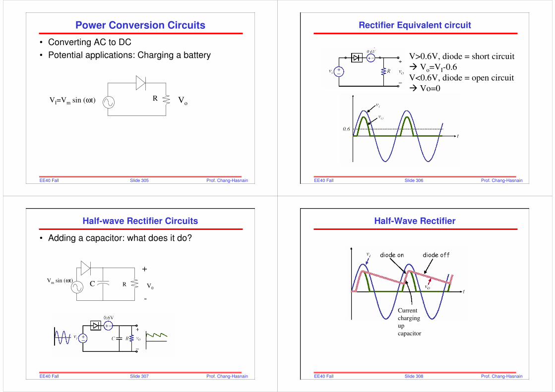
Slide 305EE40 Fall2006
Prof. Chang-Hasnain
Power Conversion Circuits
• Converting AC to DC
• Potential applications: Charging a battery
VI=Vm sin (ωt) R Vo
Slide 306EE40 Fall2006
Prof. Chang-Hasnain
Rectifier Equivalent circuit
V>0.6V, diode = short circuit
Vo=VI-0.6
V<0.6V, diode = open circuit
Vo=0
Slide 307EE40 Fall2006
Prof. Chang-Hasnain
Half-wave Rectifier Circuits
• Adding a capacitor: what does it do?
Vm sin (ωt)R V0
C
+
-
Slide 308EE40 Fall2006
Prof. Chang-Hasnain
Half-Wave Rectifier
Current
charging
up
capacitor
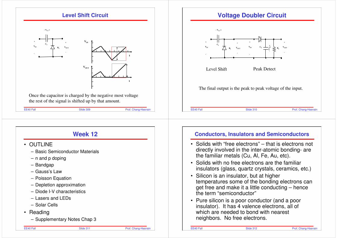
Slide 309EE40 Fall2006
Prof. Chang-Hasnain
Level Shift Circuit
- VC1 +
R1VOUT
+
-
VIN
+
-
C1
VIN
t
VOUT
t
Once the capacitor is charged by the negative most voltage
the rest of the signal is shifted up by that amount.
Slide 310EE40 Fall2006
Prof. Chang-Hasnain
Voltage Doubler Circuit
+ V
C2
1-
R2
VOUT
+
-
VIN
+
-
C2
- VC1 +
R1VOUT
+
-
VIN
+
-
C1
Level Shift Peak Detect
The final output is the peak to peak voltage of the input.
Slide 311EE40 Fall2006
Prof. Chang-Hasnain
Week 12
• OUTLINE
– Basic Semiconductor Materials
– n and p doping
– Bandgap
– Gauss’s Law
– Poisson Equation
– Depletion approximation
– Diode I-V characteristics
– Lasers and LEDs
– Solar Cells
• Reading
– Supplementary Notes Chap 3
Slide 312EE40 Fall2006
Prof. Chang-Hasnain
Conductors, Insulators and Semiconductors
• Solids with “free electrons” – that is electrons not directly involved in the inter-atomic bonding- are the familiar metals (Cu, Al, Fe, Au, etc).
• Solids with no free electrons are the familiar insulators (glass, quartz crystals, ceramics, etc.)
• Silicon is an insulator, but at higher temperatures some of the bonding electrons can get free and make it a little conducting – hence the term “semiconductor”
• Pure silicon is a poor conductor (and a poor insulator). It has 4 valence electrons, all of which are needed to bond with nearest neighbors. No free electrons.

Slide 313EE40 Fall2006
Prof. Chang-Hasnain
The Periodic Table
III IV V
Slide 314EE40 Fall2006
Prof. Chang-Hasnain
Electronic Bonds in Silicon
2-D picture of perfect crystal of pure silicon; double line is a Si-Si bond with each line representing an electron
Two electrons in each bond
Si ion(charge+4 q)
Actual structure is 3-dimensional tetrahedral- just like carbon
bonding in organic and inorganic materials.
Essentially no free electrons, and no conduction - insulator
Slide 315EE40 Fall2006
Prof. Chang-Hasnain
How to get conduction in Si?
For the first approach controlled impurities, “dopants”, are added to
Si:
or
We must either:
1) Chemically modify the Si to produce free carriers (permanent) or
2) Electrically “induce” them by the field effect (switchable)
(Extra electrons produce “free electrons” for conduction.)
Add group V elements (5 bonding electrons vs four for Si), such as phosphorus or arsenic
Deficiency of electrons results in “free holes”
Add group III elements (3 bonding electrons), such as boron
Slide 316EE40 Fall2006
Prof. Chang-Hasnain
Doping Silicon with Donors (n-type)
Donors donate mobile electrons (and thus “n-type” silicon)
Example: add arsenic (As) to the silicon crystal:
Immobile (stuck) positively charged arsenic ion after 5th electron left
As
Mobile electrondonated by As ion
The extra electron with As, “breaks free” and becomes a free
electron for conduction
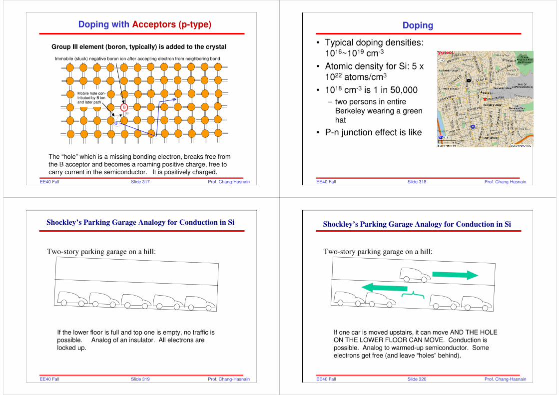
Slide 317EE40 Fall2006
Prof. Chang-Hasnain
Doping with Acceptors (p-type)
B
Mobile hole con-tributed by B ionand later path
Immobile (stuck) negative boron ion after accepting electron from neighboring bond
Group III element (boron, typically) is added to the crystal
The “hole” which is a missing bonding electron, breaks free from the B acceptor and becomes a roaming positive charge, free to carry current in the semiconductor. It is positively charged.
Slide 318EE40 Fall2006
Prof. Chang-Hasnain
Doping
• Typical doping densities:
1016~1019 cm-3
• Atomic density for Si: 5 x
1022 atoms/cm3
• 1018 cm-3 is 1 in 50,000
– two persons in entire
Berkeley wearing a green hat
• P-n junction effect is like
Slide 319EE40 Fall2006
Prof. Chang-Hasnain
If the lower floor is full and top one is empty, no traffic is possible. Analog of an insulator. All electrons are locked up.
Shockley’s Parking Garage Analogy for Conduction in Si
Two-story parking garage on a hill:
Slide 320EE40 Fall2006
Prof. Chang-Hasnain
If one car is moved upstairs, it can move AND THE HOLE ON THE LOWER FLOOR CAN MOVE. Conduction is possible. Analog to warmed-up semiconductor. Some electrons get free (and leave “holes” behind).
Shockley’s Parking Garage Analogy for Conduction in Si
Two-story parking garage on a hill:
Slide 321EE40 Fall2006
Prof. Chang-Hasnain
If an extra car is “donated” to the upper floor, it can move. Conduction is possible. Analog to N-type semiconductor.(An electron donor is added to the crystal, creating free electrons).
Shockley’s Parking Garage Analogy for Conduction in Si
Two-story parking garage on a hill:
Slide 322EE40 Fall2006
Prof. Chang-Hasnain
If a car is removed from the lower floor, it leaves a HOLE which can move. Conduction is possible. Analog to P-type semiconductor. (Acceptors are added to the crystal, “consuming” bonding electrons,creating free holes).
Shockley’s Parking Garage Analogy for Conduction in Si
Two-story parking garage on a hill:
Slide 323EE40 Fall2006
Prof. Chang-Hasnain
Summary of n- and p-type silicon
Pure silicon is an insulator. At high temperatures it conducts weakly.
If we add an impurity with extra electrons (e.g. arsenic, phosphorus) these extra electrons are set free and we have a pretty good conductor (n-type silicon).
If we add an impurity with a deficit of electrons (e.g. boron) then bonding electrons are missing (holes), and the resulting holes can move around … again a pretty good conductor (p-type silicon)
Now what is really interesting is when we join n-type and p-type silicon, that is make a pn junction. It has interesting electrical properties.
Slide 324EE40 Fall2006
Prof. Chang-Hasnain
Junctions of n- and p-type Regions
A silicon chip may have 108 to 109 p-n junctions today.
p-n junctions form the essential basis of all semiconductor devices.
How do they behave*? What happens to the electrons and holes?What is the electrical circuit model for such junctions?
n and p regions are brought into contact :
n p
aluminum aluminum
wire
?
*Note that the textbook has a very good explanation.
Slide 325EE40 Fall2006
Prof. Chang-Hasnain
The pn Junction Diode
Schematic diagram
p-type n-typeID
+ VD –
Circuit symbol
Physical structure:(an example)
p-type Si
n-type Si
SiO2SiO2
metal
metal
ID+
VD
–
net donor
concentration ND
net acceptor
concentration NA
For simplicity, assume that
the doping profile changes
abruptly at the junction.
cross-sectional area AD
Slide 326EE40 Fall2006
Prof. Chang-Hasnain
• When the junction is first formed, mobile carriers diffuseacross the junction (due to the concentration gradients)
– Holes diffuse from the p side to the n side, leaving behind negatively charged immobile acceptor ions
– Electrons diffuse from the n side to the p side, leaving behind positively charged immobile donor ions
A region depleted of mobile carriers is formed at the junction.
• The space charge due to immobile ions in the depletion region establishes an electric field that opposes carrier diffusion.
Depletion Region Approximation
+++++
––
–––
p n
acceptor ions donor ions
Slide 327EE40 Fall2006
Prof. Chang-Hasnain
Summary: pn-Junction Diode I-V
• Under forward bias, the potential barrier is reduced, so that carriers flow (by diffusion) across the junction
– Current increases exponentially with increasing forward bias
– The carriers become minority carriers once they cross the junction; as they diffuse in the quasi-neutral regions, they recombine with majority carriers (supplied by the metal contacts)
“injection” of minority carriers
• Under reverse bias, the potential barrier is increased, so that negligible carriers flow across the junction
– If a minority carrier enters the depletion region (by thermal generation or diffusion from the quasi-neutral regions), it will be swept across the junction by the built-in electric field
“collection” of minority carriers reverse current ID (A)
VD (V)
Slide 328EE40 Fall2006
Prof. Chang-Hasnain
quasi-neutral p region
Charge Density Distribution
+++++
––
–––
p n
acceptor ions donor ions
depletion region quasi-neutral n region
charge density (C/cm3)
distance
Charge is stored in the depletion region.
Slide 329EE40 Fall2006
Prof. Chang-Hasnain
Effect of Applied Voltage
• The quasi-neutral p and n regions have low resistivity, whereas the depletion region has high resistivity. Thus,
when an external voltage VD is applied across the diode,
almost all of this voltage is dropped across the depletion region. (Think of a voltage divider circuit.)
• If VD > 0 (forward bias), the potential barrier to carrier diffusion is reduced by the applied voltage.
• If VD < 0 (reverse bias), the potential barrier to carrier diffusion is increased by the applied voltage.
p n
+++++
––
–––
VD
Slide 330EE40 Fall2006
Prof. Chang-Hasnain
Forward Bias
• As VD increases, the potential barrier to carrier
diffusion across the junction decreases*, and
current increases exponentially.
ID (Amperes)
VD (Volts)
* Hence, the width of the depletion region decreases.
p n
+++++
––
–––
VD > 0The carriers that diffuse across the
junction become minority carriers in
the quasi-neutral regions; they then
recombine with majority carriers,
“dying out” with distance.
Slide 331EE40 Fall2006
Prof. Chang-Hasnain
Reverse Bias
• As |VD| increases, the potential barrier to carrier
diffusion across the junction increases*; thus, no
carriers diffuse across the junction.
ID (Amperes)
VD (Volts)
* Hence, the width of the depletion region increases.
p n
+++++
––
–––
VD < 0A very small amount of reverse
current (ID < 0) does flow, due to
minority carriers diffusing from the
quasi-neutral regions into the depletion
region and drifting across the junction.
Slide 332EE40 Fall2006
Prof. Chang-Hasnain
• Light incident on a pn junction generates electron-hole pairs
• Carriers are generated in the depletion region as well as n-doped and p-doped quasi-neutral regions.
• The carriers that are generated in the quasi-neutral regions diffuse into the depletion region, together with the carriers generated in the depletion region, are swept across the junction by the electric field
• This results in an additional component of current flowing in the diode:
where Ioptical is proportional to the intensity of the light
optical
kTVq
SD IeII −−= )1( D
Optoelectronic Diodes

Slide 333EE40 Fall2006
Prof. Chang-Hasnain
Example: Photodiode
• An intrinsic region is placed between the p-type and n-type
regions
Wj ≅ Wi-region, so that most of the electron-hole pairs are generated in the depletion region
faster response time
(~10 GHz operation)
ID (A)
VD (V)
with incident light
in the dark
operating point
Slide 334EE40 Fall2006
Prof. Chang-Hasnain
Planck Constant
• Planck’s constant h = 6.625·10-34 J·s• E=hν=hc/λ• C is speed of light and hν is photon energy• The first type of quantum effect is the quantization of
certain physical quantities.
• Quantization first arose in the mathematical formulae of Max Planck in 1900. Max Planck was analyzing how the radiation emitted from a body was related to its temperature, in other words, he was analyzing the energy of a wave.
• The energy of a wave could not be infinite, so Planck used the property of the wave we designate as the frequency to define energy. Max Planck discovered a constant that when multiplied by the frequency of any wave gives the energy of the wave. This constant is referred to by the letter h in mathematical formulae. It is a cornerstone of physics.
Slide 335EE40 Fall2006
Prof. Chang-Hasnain
Bandgap Versus Lattice Constant
Si
Slide 336EE40 Fall2006
Prof. Chang-Hasnain
Chapter 12 MOSFET
• OUTLINE– The MOSFET as a controlled resistor– Pinch-off and current saturation
– MOSFET ID vs. VGS characteristic
– NMOS and PMOS I-V characteristics– Load-line analysis; Q operating point; Bias circuits
– Small-signal equivalent circuits – Common source amplifier
– Source follower– Common gate amplifier
– Gain
• Reading– Supplementary Notes Chapter 4 – Hambley: Chapter 12.1-12.5
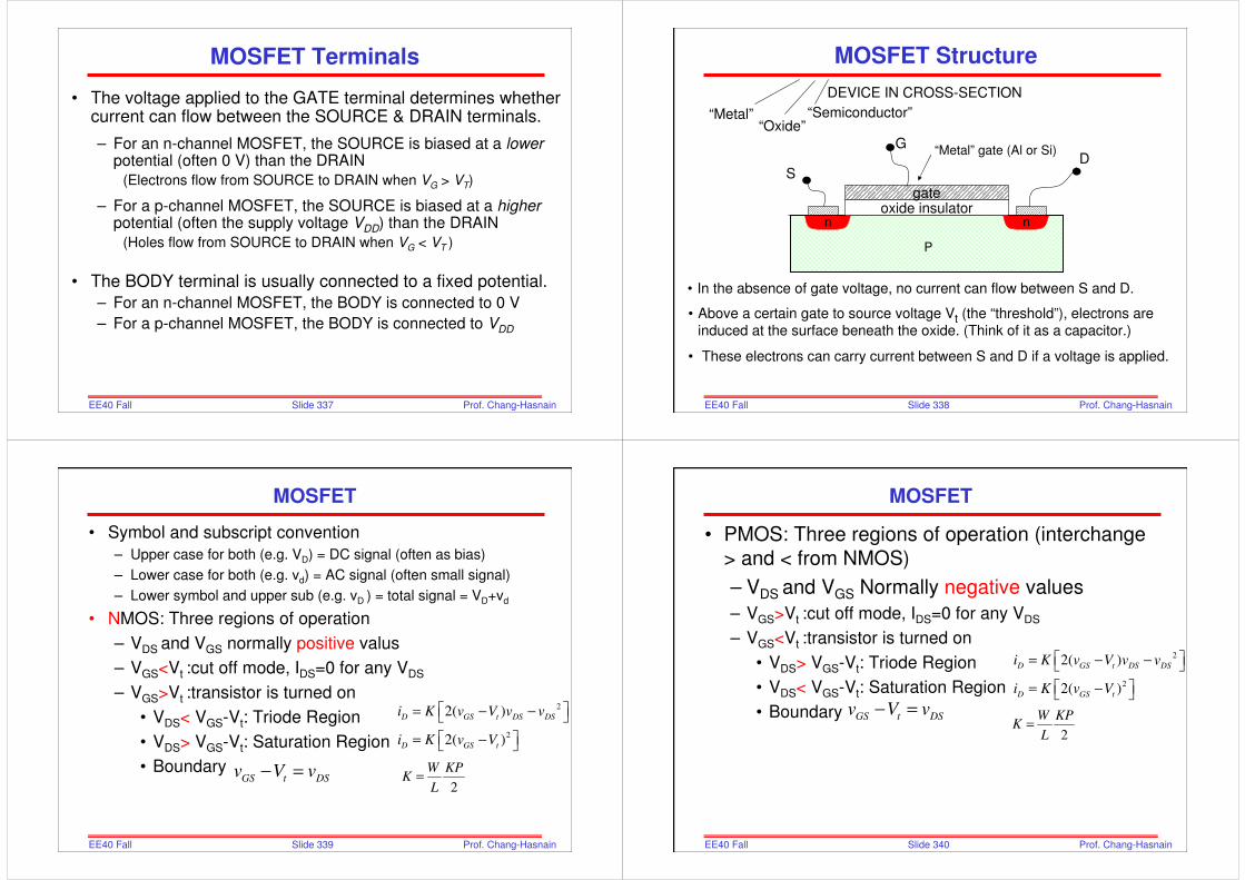
Slide 337EE40 Fall2006
Prof. Chang-Hasnain
• The voltage applied to the GATE terminal determines whether current can flow between the SOURCE & DRAIN terminals.
– For an n-channel MOSFET, the SOURCE is biased at a lowerpotential (often 0 V) than the DRAIN
(Electrons flow from SOURCE to DRAIN when VG > VT)
– For a p-channel MOSFET, the SOURCE is biased at a higherpotential (often the supply voltage VDD) than the DRAIN
(Holes flow from SOURCE to DRAIN when VG < VT )
• The BODY terminal is usually connected to a fixed potential.
– For an n-channel MOSFET, the BODY is connected to 0 V
– For a p-channel MOSFET, the BODY is connected to VDD
MOSFET Terminals
Slide 338EE40 Fall2006
Prof. Chang-Hasnain
MOSFET Structure
DEVICE IN CROSS-SECTION
“Metal” “Semiconductor”“Oxide”
• In the absence of gate voltage, no current can flow between S and D.
• Above a certain gate to source voltage Vt (the “threshold”), electrons are induced at the surface beneath the oxide. (Think of it as a capacitor.)
• These electrons can carry current between S and D if a voltage is applied.
n
P
oxide insulatorgate
n
“Metal” gate (Al or Si)D
S
G
Slide 339EE40 Fall2006
Prof. Chang-Hasnain
MOSFET
• Symbol and subscript convention
– Upper case for both (e.g. VD) = DC signal (often as bias)
– Lower case for both (e.g. vd) = AC signal (often small signal)
– Lower symbol and upper sub (e.g. vD ) = total signal = VD+vd
• NMOS: Three regions of operation
– VDS and VGS normally positive valus
– VGS<Vt :cut off mode, IDS=0 for any VDS
– VGS>Vt :transistor is turned on
• VDS< VGS-Vt: Triode Region
• VDS> VGS-Vt: Saturation Region
• Boundary
2
2
2( )
2( )
D GS t DS DS
D GS t
i K v V v v
i K v V
= − −
= −
GS t DSv V v− =
2
W KPK
L=
Slide 340EE40 Fall2006
Prof. Chang-Hasnain
MOSFET
• PMOS: Three regions of operation (interchange
> and < from NMOS)
– VDS and VGS Normally negative values
– VGS>Vt :cut off mode, IDS=0 for any VDS
– VGS<Vt :transistor is turned on
• VDS> VGS-Vt: Triode Region
• VDS< VGS-Vt: Saturation Region
• Boundary
2
2
2( )
2( )
D GS t DS DS
D GS t
i K v V v v
i K v V
= − −
= −
GS t DSv V v− =
2
W KPK
L=
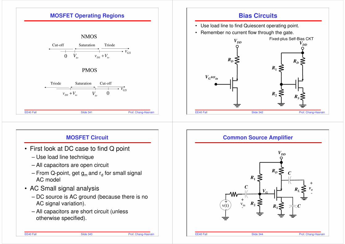
Slide 341EE40 Fall2006
Prof. Chang-Hasnain
MOSFET Operating Regions
DS tov V+0
GSv
TriodeSaturationCut-off
toV
NMOS
DS tov V+ 0
GSv
Triode Saturation Cut-off
toV
PMOS
Slide 342EE40 Fall2006
Prof. Chang-Hasnain
Bias Circuits
• Use load line to find Quiescent operating point.
• Remember no current flow through the gate.
VDD
RD
R1
R2 RS
VDD
RD
VG+vin
Fixed-plus Self-Bias CKT
Slide 343EE40 Fall2006
Prof. Chang-Hasnain
MOSFET Circuit
• First look at DC case to find Q point
– Use load line technique
– All capacitors are open circuit
– From Q-point, get gm and rd for small signal
AC model
• AC Small signal analysis
– DC source is AC ground (because there is no
AC signal variation).
– All capacitors are short circuit (unless
otherwise specified).
Slide 344EE40 Fall2006
Prof. Chang-Hasnain
Common Source Amplifier
VDD
RD
R1
R2 RS C
C
RL
+
-vo
C
+
-vin
+
-v(t)
VG
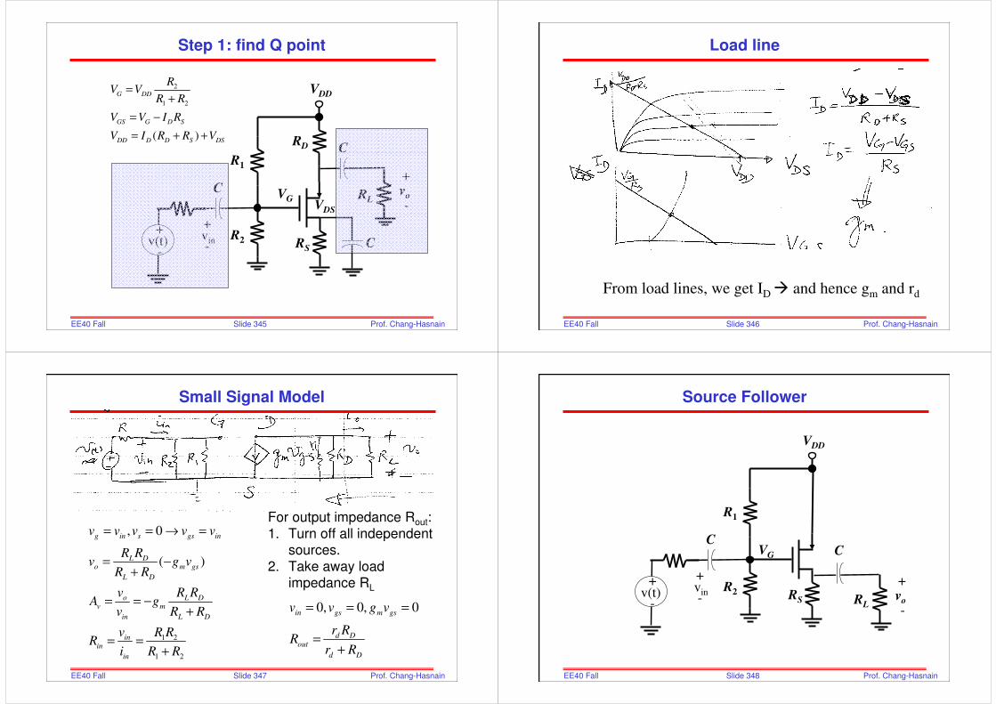
Slide 345EE40 Fall2006
Prof. Chang-Hasnain
Step 1: find Q point
VDD
RD
R1
R2 RS C
C
RL
+
-vo
C
+
-vin
+
-v(t)
VGVDS
2
1 2
( )
G DD
GS G D S
DD D D S DS
RV V
R R
V V I R
V I R R V
=+
= −
= + +
Slide 346EE40 Fall2006
Prof. Chang-Hasnain
Load line
From load lines, we get ID and hence gm and rd
Slide 347EE40 Fall2006
Prof. Chang-Hasnain
Small Signal Model
1 2
1 2
, 0
( )
g in s gs in
L Do m gs
L D
o L Dv m
in L D
inin
in
v v v v v
R Rv g v
R R
v R RA g
v R R
v R RR
i R R
= = → =
= −+
= = −+
= =+
For output impedance Rout:
1. Turn off all independent sources.
2. Take away load impedance RL
0, 0, 0in gs m gs
d Dout
d D
v v g v
r RR
r R
= = =
=+
Slide 348EE40 Fall2006
Prof. Chang-Hasnain
Source Follower
VDD
R1
R2 RS
C
RL
+
-vo
C
+
-vin
+
-v(t)
VG

Slide 349EE40 Fall2006
Prof. Chang-Hasnain
Step 1: find Q point
2
1 2
G DD
GS G D S
DD D S DS
RV V
R R
V V I R
V I R V
=+
= −
= +
VDD
R1
R2 RS
C
RL
+
-vo
C
+
-vin
+
-v(t)
VG
Slide 350EE40 Fall2006
Prof. Chang-Hasnain
Load line
From load lines, we get ID and hence gm and rd
Slide 351EE40 Fall2006
Prof. Chang-Hasnain
Small Signal Model
1 1 1
1 2
1 2
1
(1 )
1
L
d S L
gs in o
o m gs L
in gs m L
o m Lv
in m L
inin
in
Rr R R
v v v
v g v R
v v g R
v g RA
v g R
v R RR
i R R
− − −′ =
+ +
= −
′=
′= +
′= =
′+
= =+
For output impedance Rout:1. Turn off all independent sources.2. Take away RL
3. Add Vx and find ix
( )1
1 1
, 0,
, ( )
1
x s g gs x
d s xs x m x x s m
d s s
out
m d s
v v v v v
r R vR i g v v R g
r R R
Rg r R
−
− −
= = = −
′ ′= = − − = ++ ′
=+ +
Slide 352EE40 Fall2006
Prof. Chang-Hasnain
Common Gate Amplifier
VDD
RD
RS
C
RL
+
-vo
C+
-vin
+
-v(t)
VG
-VSS
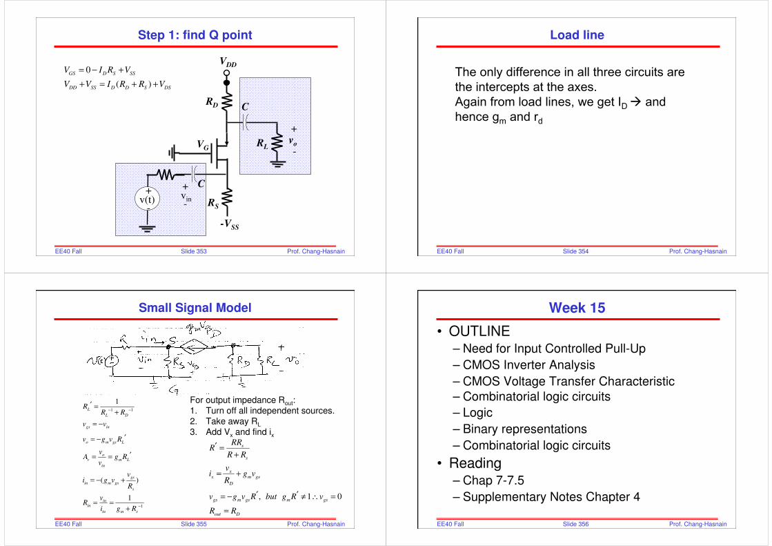
Slide 353EE40 Fall2006
Prof. Chang-Hasnain
Step 1: find Q point
VDD
RD
RS
C
RL
+
-vo
C+
-vin
+
-v(t)
VG
-VSS
0
( )
GS D S SS
DD SS D D S DS
V I R V
V V I R R V
= − +
+ = + +
Slide 354EE40 Fall2006
Prof. Chang-Hasnain
Load line
The only difference in all three circuits are the intercepts at the axes.Again from load lines, we get ID and hence gm and rd
Slide 355EE40 Fall2006
Prof. Chang-Hasnain
Small Signal Model
1 1
1
1
( )
1
L
L D
gs in
o m gs L
ov m L
in
gs
in m gs
s
inin
in m s
RR R
v v
v g v R
vA g R
v
vi g v
R
vR
i g R
− −
−
′ =+
= −
′= −
′= =
= − +
= =+
For output impedance Rout:1. Turn off all independent sources.2. Take away RL
3. Add Vx and find ix
, 1 0
s
s
xx m gs
D
gs m gs m gs
out D
RRR
R R
vi g v
R
v g v R but g R v
R R
′ =+
= +
′ ′= − ≠ ∴ =
=
Slide 356EE40 Fall2006
Prof. Chang-Hasnain
Week 15
• OUTLINE– Need for Input Controlled Pull-Up
– CMOS Inverter Analysis
– CMOS Voltage Transfer Characteristic
– Combinatorial logic circuits
– Logic
– Binary representations
– Combinatorial logic circuits
• Reading– Chap 7-7.5
– Supplementary Notes Chapter 4
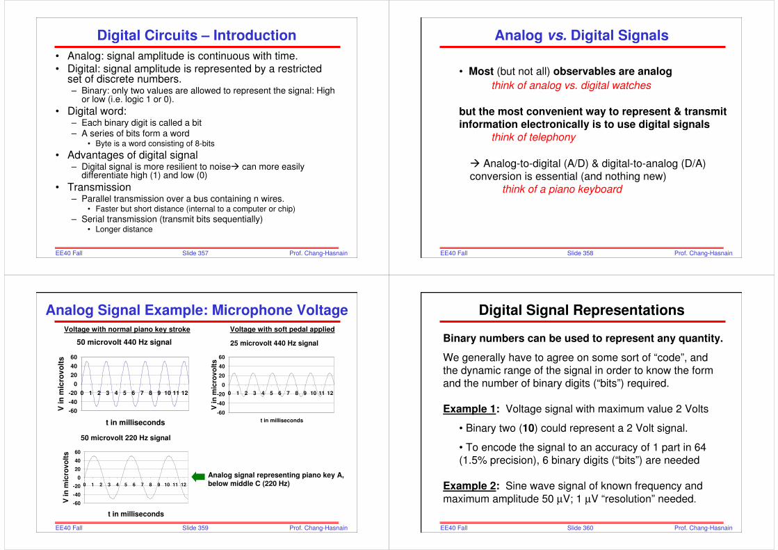
Slide 357EE40 Fall2006
Prof. Chang-Hasnain
Digital Circuits – Introduction
• Analog: signal amplitude is continuous with time.• Digital: signal amplitude is represented by a restricted
set of discrete numbers.– Binary: only two values are allowed to represent the signal: High
or low (i.e. logic 1 or 0).
• Digital word:– Each binary digit is called a bit– A series of bits form a word
• Byte is a word consisting of 8-bits
• Advantages of digital signal– Digital signal is more resilient to noise can more easily
differentiate high (1) and low (0)
• Transmission– Parallel transmission over a bus containing n wires.
• Faster but short distance (internal to a computer or chip)
– Serial transmission (transmit bits sequentially)• Longer distance
Slide 358EE40 Fall2006
Prof. Chang-Hasnain
Analog-to-digital (A/D) & digital-to-analog (D/A) conversion is essential (and nothing new)
think of a piano keyboard
• Most (but not all) observables are analog
think of analog vs. digital watches
but the most convenient way to represent & transmit information electronically is to use digital signals
think of telephony
Analog vs. Digital Signals
Slide 359EE40 Fall2006
Prof. Chang-Hasnain
Voltage with normal piano key stroke Voltage with soft pedal applied
50 microvolt 220 Hz signal
-60
-40
-20
0
20
40
60
0 1 2 3 4 5 6 7 8 9 10 11 12
t in milliseconds
V in
mic
rov
olt
s
50 microvolt 440 Hz signal
-60
-40
-20
0
20
40
60
0 1 2 3 4 5 6 7 8 9 10 11 12
t in milliseconds
V in
mic
rov
olt
s
25 microvolt 440 Hz signal
-60
-40
-20
0
20
40
60
0 1 2 3 4 5 6 7 8 9 10 11 12
t in milliseconds
V in
mic
rov
olt
s
Analog Signal Example: Microphone Voltage
Analog signal representing piano key A, below middle C (220 Hz)
Slide 360EE40 Fall2006
Prof. Chang-Hasnain
Digital Signal Representations
Binary numbers can be used to represent any quantity.
We generally have to agree on some sort of “code”, and
the dynamic range of the signal in order to know the form
and the number of binary digits (“bits”) required.
Example 1: Voltage signal with maximum value 2 Volts
• Binary two (10) could represent a 2 Volt signal.
• To encode the signal to an accuracy of 1 part in 64
(1.5% precision), 6 binary digits (“bits”) are needed
Example 2: Sine wave signal of known frequency and
maximum amplitude 50 µV; 1 µV “resolution” needed.
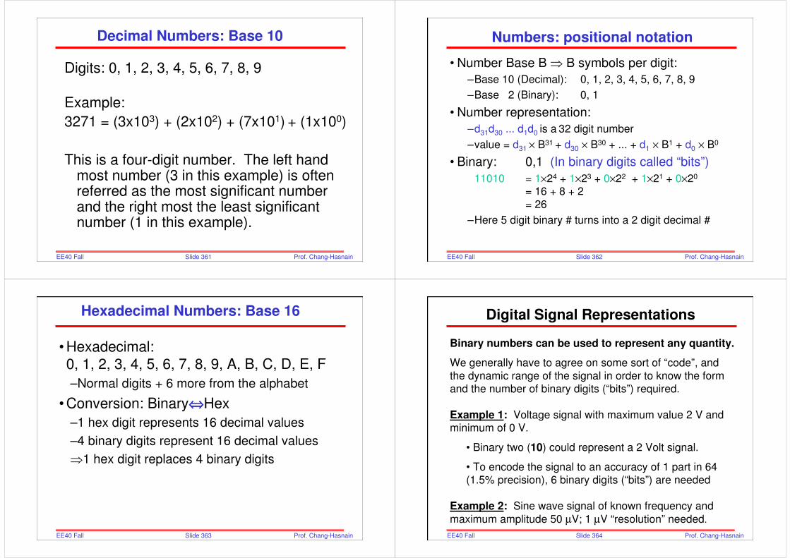
Slide 361EE40 Fall2006
Prof. Chang-Hasnain
Decimal Numbers: Base 10
Digits: 0, 1, 2, 3, 4, 5, 6, 7, 8, 9
Example:
3271 = (3x10³) + (2x10²) + (7x101) + (1x100)
This is a four-digit number. The left hand most number (3 in this example) is often referred as the most significant number and the right most the least significant number (1 in this example).
Slide 362EE40 Fall2006
Prof. Chang-Hasnain
Numbers: positional notation
• Number Base B ⇒ B symbols per digit:
–Base 10 (Decimal): 0, 1, 2, 3, 4, 5, 6, 7, 8, 9
–Base 2 (Binary): 0, 1
• Number representation:
–d31d30 ... d1d0 is a 32 digit number
–value = d31 × B31 + d30 × B30 + ... + d1 × B1 + d0 × B0
• Binary: 0,1 (In binary digits called “bits”)
11010 = 1×24 + 1×23 + 0×22 + 1×21 + 0×20
= 16 + 8 + 2
= 26
–Here 5 digit binary # turns into a 2 digit decimal #
Slide 363EE40 Fall2006
Prof. Chang-Hasnain
Hexadecimal Numbers: Base 16
• Hexadecimal: 0, 1, 2, 3, 4, 5, 6, 7, 8, 9, A, B, C, D, E, F
–Normal digits + 6 more from the alphabet
• Conversion: Binary⇔⇔⇔⇔Hex
–1 hex digit represents 16 decimal values
–4 binary digits represent 16 decimal values
⇒1 hex digit replaces 4 binary digits
Slide 364EE40 Fall2006
Prof. Chang-Hasnain
Digital Signal Representations
Binary numbers can be used to represent any quantity.
We generally have to agree on some sort of “code”, and
the dynamic range of the signal in order to know the form
and the number of binary digits (“bits”) required.
Example 1: Voltage signal with maximum value 2 V and minimum of 0 V.
• Binary two (10) could represent a 2 Volt signal.
• To encode the signal to an accuracy of 1 part in 64
(1.5% precision), 6 binary digits (“bits”) are needed
Example 2: Sine wave signal of known frequency and
maximum amplitude 50 µV; 1 µV “resolution” needed.
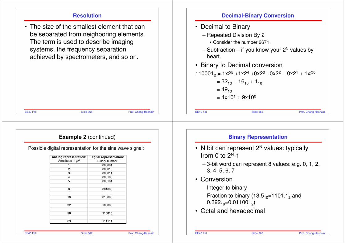
Slide 365EE40 Fall2006
Prof. Chang-Hasnain
Resolution
• The size of the smallest element that can be separated from neighboring elements. The term is used to describe imaging systems, the frequency separation achieved by spectrometers, and so on.
Slide 366EE40 Fall2006
Prof. Chang-Hasnain
Decimal-Binary Conversion
• Decimal to Binary
– Repeated Division By 2
• Consider the number 2671.
– Subtraction – if you know your 2N values by
heart.
• Binary to Decimal conversion
1100012 = 1x25 +1x24 +0x23 +0x22 + 0x21 + 1x20
= 3210 + 1610 + 110
= 4910
= 4x101 + 9x100
Slide 367EE40 Fall2006
Prof. Chang-Hasnain
Possible digital representation for the sine wave signal:
Analog representation: Digital representation:Amplitude in µV Binary number
1 000001
2 000010
3 000011
4 000100
5 000101
8 001000
16 010000
32 100000
50 110010
63 111111
Example 2 (continued)
Slide 368EE40 Fall2006
Prof. Chang-Hasnain
Binary Representation
• N bit can represent 2N values: typically from 0 to 2N-1
– 3-bit word can represent 8 values: e.g. 0, 1, 2,
3, 4, 5, 6, 7
• Conversion
– Integer to binary
– Fraction to binary (13.510=1101.12 and
0.39210=0.0110012)
• Octal and hexadecimal
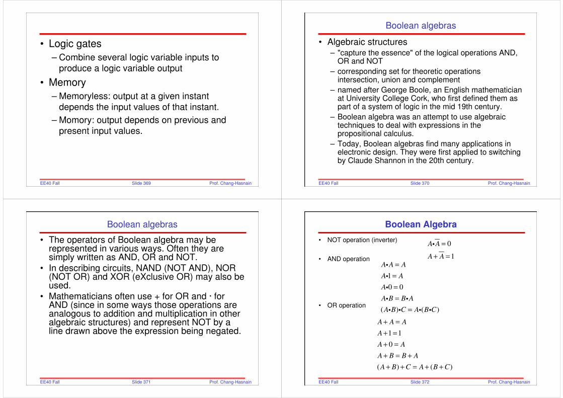
Slide 369EE40 Fall2006
Prof. Chang-Hasnain
• Logic gates
– Combine several logic variable inputs to
produce a logic variable output
• Memory
– Memoryless: output at a given instant
depends the input values of that instant.
– Momory: output depends on previous and
present input values.
Slide 370EE40 Fall2006
Prof. Chang-Hasnain
Boolean algebras
• Algebraic structures– "capture the essence" of the logical operations AND,
OR and NOT
– corresponding set for theoretic operations intersection, union and complement
– named after George Boole, an English mathematician at University College Cork, who first defined them as part of a system of logic in the mid 19th century.
– Boolean algebra was an attempt to use algebraic techniques to deal with expressions in the propositional calculus.
– Today, Boolean algebras find many applications in electronic design. They were first applied to switchingby Claude Shannon in the 20th century.
Slide 371EE40 Fall2006
Prof. Chang-Hasnain
Boolean algebras
• The operators of Boolean algebra may be represented in various ways. Often they are simply written as AND, OR and NOT.
• In describing circuits, NAND (NOT AND), NOR (NOT OR) and XOR (eXclusive OR) may also be used.
• Mathematicians often use + for OR and · for AND (since in some ways those operations are analogous to addition and multiplication in other algebraic structures) and represent NOT by a line drawn above the expression being negated.
Slide 372EE40 Fall2006
Prof. Chang-Hasnain
Boolean Algebra
• NOT operation (inverter)
• AND operation
• OR operation
0
1
A A
A A
=
+ =
i
1
0 0
( ) ( )
A A A
A A
A
A B B A
A B C A B C
=
=
=
=
=
i
i
i
i i
i i i i
1 1
0
( ) ( )
A A A
A
A A
A B B A
A B C A B C
+ =
+ =
+ =
+ = +
+ + = + +
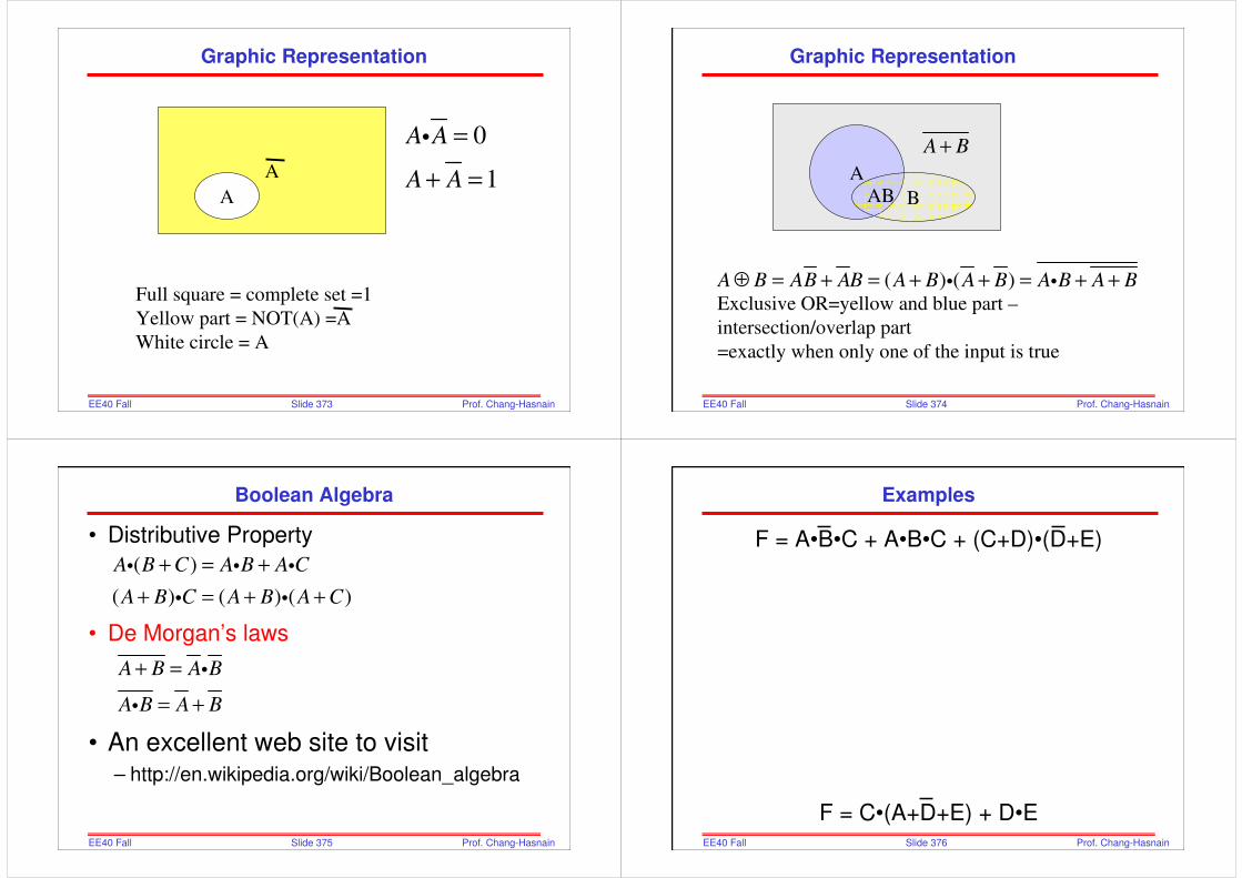
Slide 373EE40 Fall2006
Prof. Chang-Hasnain
Graphic Representation
A
A
0
1
A A
A A
=
+ =
i
Full square = complete set =1
Yellow part = NOT(A) =A
White circle = A
Slide 374EE40 Fall2006
Prof. Chang-Hasnain
Graphic Representation
A
BAB
A B+
( ) ( )A B AB AB A B A B A B A B⊕ = + = + + = + +i i
Exclusive OR=yellow and blue part –
intersection/overlap part
=exactly when only one of the input is true
Slide 375EE40 Fall2006
Prof. Chang-Hasnain
Boolean Algebra
• Distributive Property
• De Morgan’s laws
• An excellent web site to visit– http://en.wikipedia.org/wiki/Boolean_algebra
( )
( ) ( ) ( )
A B C A B A C
A B C A B A C
+ = +
+ = + +
i i i
i i
A B A B
A B A B
+ =
= +
i
i
Slide 376EE40 Fall2006
Prof. Chang-Hasnain
F = A•B•C + A•B•C + (C+D)•(D+E)
F = C•(A+D+E) + D•E
Examples
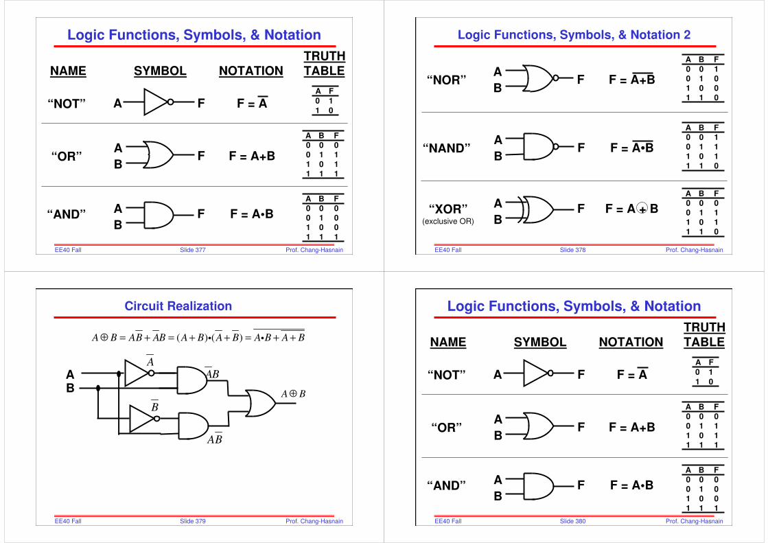
Slide 377EE40 Fall2006
Prof. Chang-Hasnain
Logic Functions, Symbols, & Notation
“NOT” F = A
TRUTHNAME SYMBOL NOTATION TABLE
FA
111001010000FBA
“OR” F = A+BFA
B
01
10
FA
111101110000FBA
“AND” F = A•BFA
B
Slide 378EE40 Fall2006
Prof. Chang-Hasnain
Logic Functions, Symbols, & Notation 2
“NOR” F = A+B
011101110000FBA
“NAND” F = A•BFA
B011101110100FBA
“XOR”(exclusive OR)
F = A + BFA
B
FA
B011001010100FBA
Slide 379EE40 Fall2006
Prof. Chang-Hasnain
Circuit Realization
A B⊕
( ) ( )A B AB AB A B A B A B A B⊕ = + = + + = + +i i
AA
AB
AB
B
B
Slide 380EE40 Fall2006
Prof. Chang-Hasnain
TRUTHNAME SYMBOL NOTATION TABLE
Logic Functions, Symbols, & Notation
“NOT” F = AFA
111001010000FBA
“OR” F = A+BFA
B
01
10
FA
111101110000FBA
“AND” F = A•BFA
B

Slide 381EE40 Fall2006
Prof. Chang-Hasnain
Logic Functions, Symbols, & Notation 2
“NOR” F = A+B
011101110000FBA
“NAND” F = A•BFA
B011101110100FBA
“XOR”(exclusive OR)
F = A + BFA
B
FA
B011001010100FBA
Slide 382EE40 Fall2006
Prof. Chang-Hasnain
Fan in/Fan out
• Complex digital operations are formed with a variety of gates interconnected to yield the desired logic function.
• Sometimes a number of inputs are connected to one gate input and output of a gate may be connected to a number of gates.
• Fan-in: the maximum number of logic gates that can be connected at the input of a gate without altering its performance.
• Fan-out: the maximum number of logic gates that can be connected to the output of a gate without altering its performance.
• Typical fan-in and fan-out numbers are 3.
Slide 383EE40 Fall2006
Prof. Chang-Hasnain
Inverter = NOT Gate
VoutVin
Vin
Vout
VV/2
Ideal Transfer Characteristics
Slide 384EE40 Fall2006
Prof. Chang-Hasnain
Terminology for a Logic Circuit
VIN
VOUT
IOUT Output
RPULL UP
Pull-Down
(NMOS)
VOUT-SAT-D = Value of VOUT beyond which the current IOUT-D
saturates at the (drain) current saturation value IOUT-SAT-D.
Pull-Up Network = Set of devices used to
carry current from the power supply to
the output node to charge the output
node to the power supply voltage.
Pull-Down Network = Set of devices used to
carry current from the output node to ground to
discharge the output node to ground.
VDD
VDD = Power supply voltage (D is from
Drain) we do not draw the symbol.
IOUT = Current for the device under study.
VTD = Threshold Voltage value of VIN at which the
Pull-Down (NMOS transistor) begins to conduct.
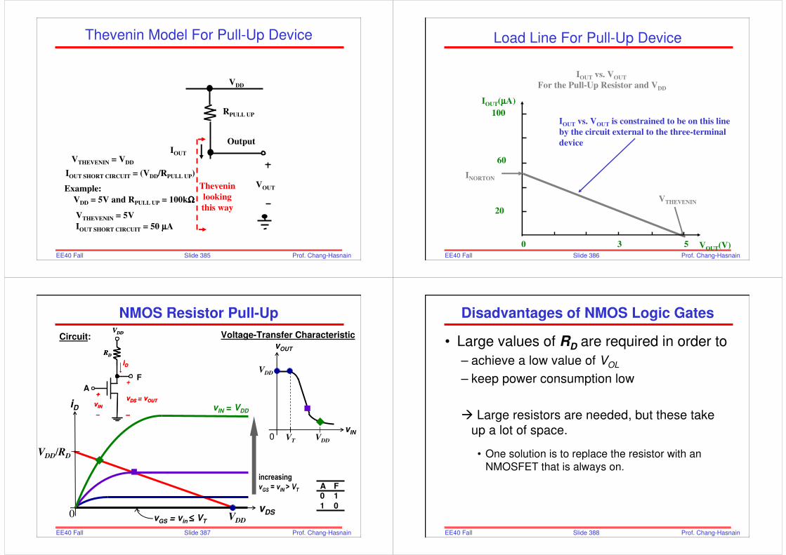
Slide 385EE40 Fall2006
Prof. Chang-Hasnain
Thevenin Model For Pull-Up Device
VTHEVENIN = VDD
IOUT SHORT CIRCUIT = (VDD/RPULL UP)
VOUT
IOUT
Output
VDD
RPULL UP
Example:
VDD = 5V and RPULL UP = 100kΩΩΩΩ
VTHEVENIN = 5V
IOUT SHORT CIRCUIT = 50 µµµµA
Thevenin
looking
this way
Slide 386EE40 Fall2006
Prof. Chang-Hasnain
Load Line For Pull-Up Device
IOUT(µµµµA)
20
60
100
VTHEVENIN
INORTON
IOUT vs. VOUT
For the Pull-Up Resistor and VDD
VOUT(V)0 3 5
IOUT vs. VOUT is constrained to be on this line
by the circuit external to the three-terminal
device
Slide 387EE40 Fall2006
Prof. Chang-Hasnain
VDD/RD
VDD
NMOS Resistor Pull-Up
vDS
iD
0
vOUT
vIN0
VDD
RD
+
vDS = vOUT
–
iD
+
vIN
–
VDD
RD
+
vDS = vOUT
–
iD
+
vIN
–
Circuit: Voltage-Transfer Characteristic
VDD
VT
01
10FA
A
F
increasing
vGS = vIN > VT
vGS = vin ≤≤≤≤ VT
vIN = VDD
VDD
Slide 388EE40 Fall2006
Prof. Chang-Hasnain
Disadvantages of NMOS Logic Gates
• Large values of RD are required in order to
– achieve a low value of VOL
– keep power consumption low
Large resistors are needed, but these take
up a lot of space.
• One solution is to replace the resistor with an
NMOSFET that is always on.
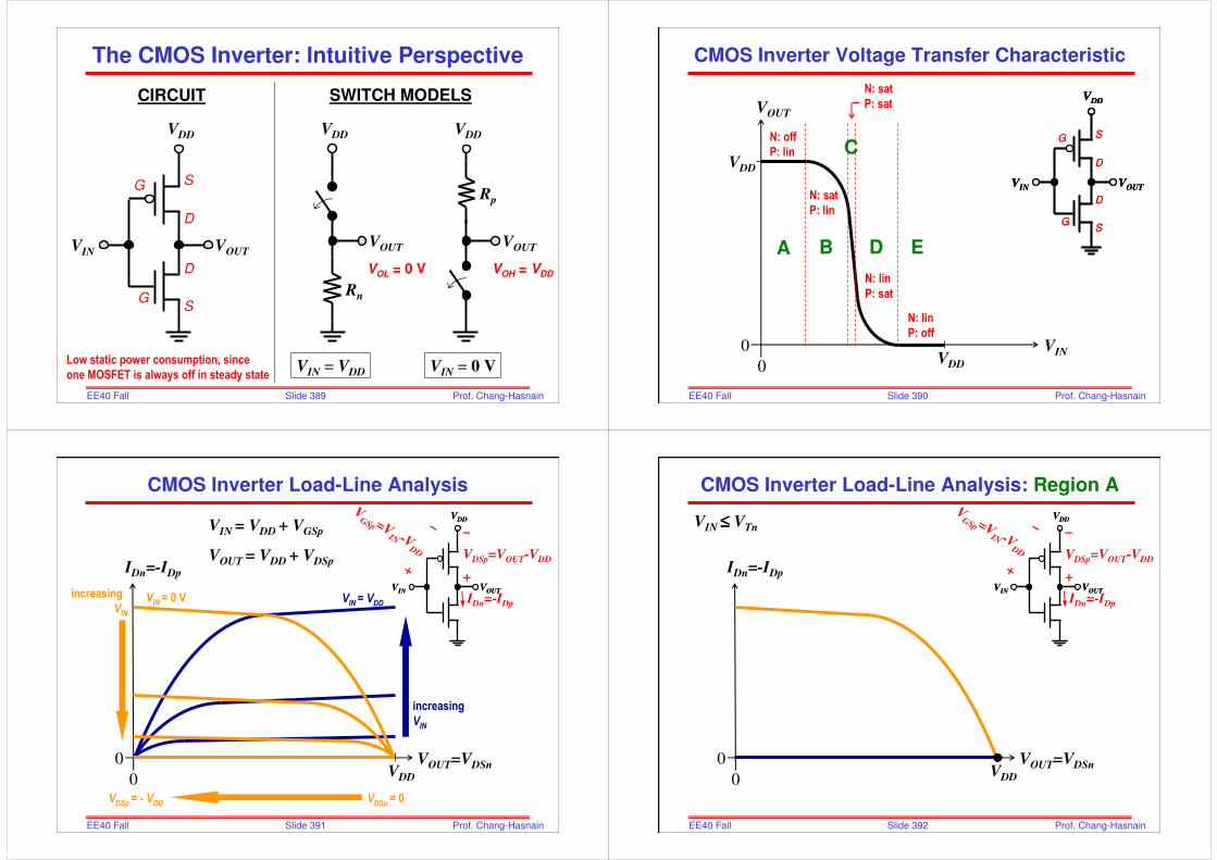
Slide 389EE40 Fall2006
Prof. Chang-Hasnain
The CMOS Inverter: Intuitive Perspective
VDD
Rn
VIN = VDD
CIRCUIT SWITCH MODELS
VDD
Rp
VIN = 0 V
VOUT VOUT
VOL = 0 V VOH = VDD
Low static power consumption, since
one MOSFET is always off in steady state
VDD
VIN VOUT
S
D
G
GS
D
Slide 390EE40 Fall2006
Prof. Chang-Hasnain
CMOS Inverter Voltage Transfer Characteristic
VIN
VOUT
VDD
VDD0
0
N: off
P: lin
N: lin
P: off
N: lin
P: sat
N: sat
P: lin
N: sat
P: satVDD
VIN VOUT
S
D
G
GS
D
VDD
VIN VOUT
VDD
VIN VOUT
S
D
G
GS
D
A B D E
C
Slide 391EE40 Fall2006
Prof. Chang-Hasnain
CMOS Inverter Load-Line Analysis
VOUT=VDSn
IDn=-IDp
0
VDD
VIN VOUT
VDD
VIN VOUT
IDn=-IDp
–V
GSp =VIN -V
DD
+
VIN = VDD + VGSp
increasing
VIN
increasing
VINVIN = 0 V VIN = VDD
VDD
VOUT = VDD + VDSp
VDSp = 0VDSp = - VDD
–
VDSp=VOUT-VDD
+
0
Slide 392EE40 Fall2006
Prof. Chang-Hasnain
VOUT=VDSn
IDn=-IDp
0VDD
0
CMOS Inverter Load-Line Analysis: Region A
VDD
VIN VOUT
VDD
VIN VOUT
IDn=-IDp
–V
GSp =VIN -V
DD
+
–
VDSp=VOUT-VDD
+
VIN ≤≤≤≤ VTn

Slide 393EE40 Fall2006
Prof. Chang-Hasnain
VOUT=VDSn
IDn=-IDp
0VDD
0
CMOS Inverter Load-Line Analysis: Region B
VDD
VIN VOUT
VDD
VIN VOUT
IDn=-IDp
–V
GSp =VIN -V
DD
+
–
VDSp=VOUT-VDD
+
VDD/2 > VIN > VTn
Slide 394EE40 Fall2006
Prof. Chang-Hasnain
VOUT=VDSn
IDn=-IDp
0VDD
0
CMOS Inverter Load-Line Analysis: Region D
VDD
VIN VOUT
VDD
VIN VOUT
IDn=-IDp
–V
GSp =VIN -V
DD
+
–
VDSp=VOUT-VDD
+
VDD – |VTp| > VIN > VDD/2
Slide 395EE40 Fall2006
Prof. Chang-Hasnain
VOUT=VDSn
IDn=-IDp
0VDD
0
CMOS Inverter Load-Line Analysis: Region E
VDD
VIN VOUT
VDD
VIN VOUT
IDn=-IDp
–V
GSp =VIN -V
DD
+
–
VDSp=VOUT-VDD
+
VIN > VDD – |VTp|
Slide 396EE40 Fall2006
Prof. Chang-Hasnain
Features of CMOS Digital Circuits
• The output is always connected to VDD or GNDin steady state
→ Full logic swing; large noise margins
→ Logic levels are not dependent upon the relative
sizes of the devices (“ratioless”)
• There is no direct path between VDD and GNDin steady state
→ no static power dissipation
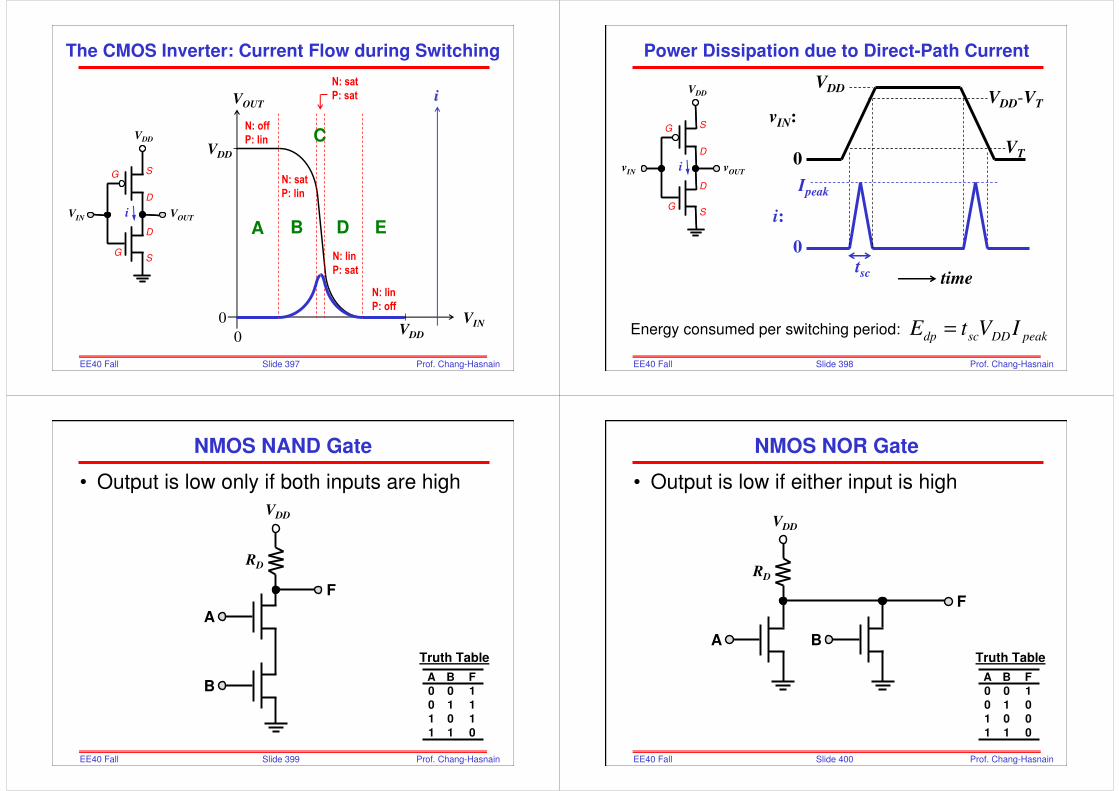
Slide 397EE40 Fall2006
Prof. Chang-Hasnain
The CMOS Inverter: Current Flow during Switching
VIN
VOUT
VDD
VDD0
0
N: off
P: lin
N: lin
P: off
N: lin
P: sat
N: sat
P: lin
N: sat
P: sat
A B D E
C
ii
i
S
D
G
GS
D
VDD
VOUTVIN
Slide 398EE40 Fall2006
Prof. Chang-Hasnain
Power Dissipation due to Direct-Path Current
VDD-VT
VT
time
vIN:
i:
Ipeak
VDD
0
0
i
S
D
G
GS
D
VDD
vOUTvIN
peakDDscdp IVtE =Energy consumed per switching period:
tsc
Slide 399EE40 Fall2006
Prof. Chang-Hasnain
NMOS NAND Gate
• Output is low only if both inputs are high
VDD
RD
A
B
F
011101110100FBA
Truth Table
Slide 400EE40 Fall2006
Prof. Chang-Hasnain
NMOS NOR Gate
• Output is low if either input is high
VDD
RD
A B
F
011001010100FBA
Truth Table
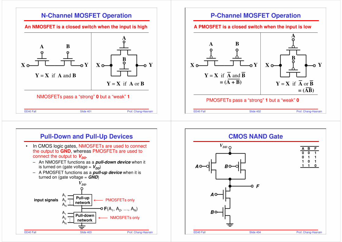
Slide 401EE40 Fall2006
Prof. Chang-Hasnain
An NMOSFET is a closed switch when the input is high
N-Channel MOSFET Operation
NMOSFETs pass a “strong” 0 but a “weak” 1
Y = X if A and B
Y = X if A or B
BA
XB
A
XY Y
Slide 402EE40 Fall2006
Prof. Chang-Hasnain
A PMOSFET is a closed switch when the input is low
P-Channel MOSFET Operation
PMOSFETs pass a “strong” 1 but a “weak” 0
Y = X if A and B
= (A + B) Y = X if A or B
= (AB)
BA
X
B
A
XY Y
Slide 403EE40 Fall2006
Prof. Chang-Hasnain
Pull-Down and Pull-Up Devices
• In CMOS logic gates, NMOSFETs are used to connect the output to GND, whereas PMOSFETs are used to connect the output to VDD.
– An NMOSFET functions as a pull-down device when it is turned on (gate voltage = VDD)
– A PMOSFET functions as a pull-up device when it is turned on (gate voltage = GND)
F(A1, A2, …, AN)
PMOSFETs only
NMOSFETs only
……
Pull-upnetwork
Pull-downnetwork
VDD
A1
A2
AN
A1
A2
AN
input signals
Slide 404EE40 Fall2006
Prof. Chang-Hasnain
CMOS NAND Gate
011101110100FBA
A
F
B
A B
VDD
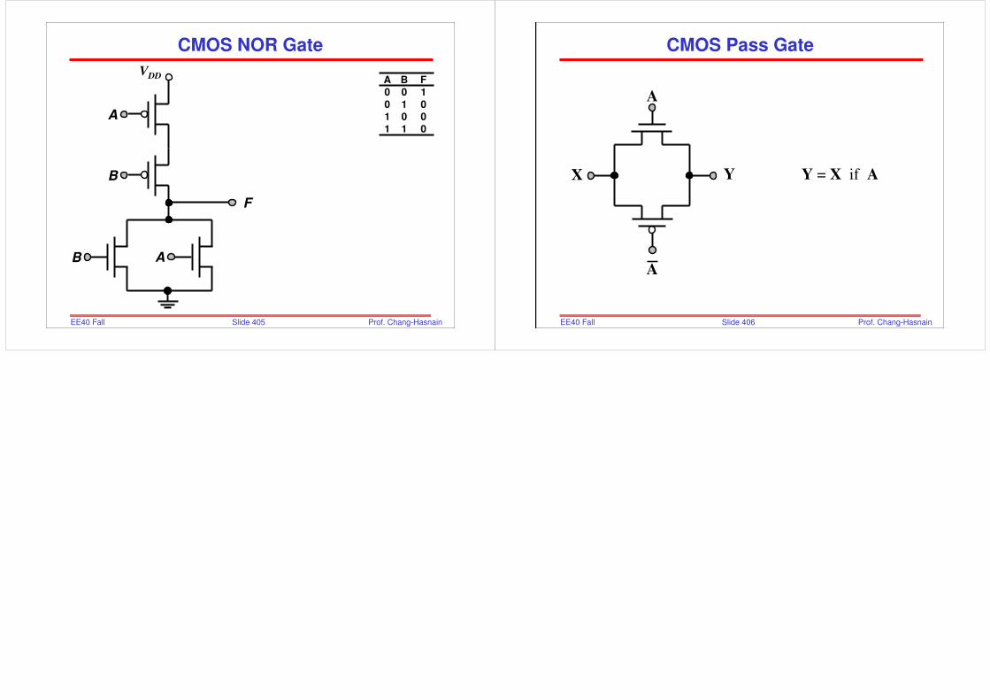
Slide 405EE40 Fall2006
Prof. Chang-Hasnain
CMOS NOR Gate
A
F
B
A
B
VDD
011001010100FBA
Slide 406EE40 Fall2006
Prof. Chang-Hasnain
CMOS Pass Gate
A
X Y
A
Y = X if A


