38


Lecture Notes in Electrical Engineering 233
For further volumes:http://www.springer.com/series/7818

Mourad Fakhfakh, Esteban Tlelo-Cuautle, andRafael Castro-López (Eds.)
Analog/RF andMixed-Signal CircuitSystematic Design
ABC

EditorsMourad FakhfakhUniversity of SfaxSfaxTunisia
Esteban Tlelo-CuautleINAOEDepartment of ElectronicsPueblaMexico
Rafael Castro-LópezInstituto de Microelectrónica de SevillaIMSE-CNM, CSIC. c/ AméricoVespucio, s/nSevilleSpain
ISSN 1876-1100 e-ISSN 1876-1119ISBN 978-3-642-36328-3 e-ISBN 978-3-642-36329-0DOI 10.1007/978-3-642-36329-0Springer Heidelberg New York Dordrecht London
Library of Congress Control Number: 2012956292
c© Springer-Verlag Berlin Heidelberg 2013This work is subject to copyright. All rights are reserved by the Publisher, whether the whole or part ofthe material is concerned, specifically the rights of translation, reprinting, reuse of illustrations, recitation,broadcasting, reproduction on microfilms or in any other physical way, and transmission or informationstorage and retrieval, electronic adaptation, computer software, or by similar or dissimilar methodologynow known or hereafter developed. Exempted from this legal reservation are brief excerpts in connectionwith reviews or scholarly analysis or material supplied specifically for the purpose of being enteredand executed on a computer system, for exclusive use by the purchaser of the work. Duplication ofthis publication or parts thereof is permitted only under the provisions of the Copyright Law of thePublisher’s location, in its current version, and permission for use must always be obtained from Springer.Permissions for use may be obtained through RightsLink at the Copyright Clearance Center. Violationsare liable to prosecution under the respective Copyright Law.The use of general descriptive names, registered names, trademarks, service marks, etc. in this publicationdoes not imply, even in the absence of a specific statement, that such names are exempt from the relevantprotective laws and regulations and therefore free for general use.While the advice and information in this book are believed to be true and accurate at the date of pub-lication, neither the authors nor the editors nor the publisher can accept any legal responsibility for anyerrors or omissions that may be made. The publisher makes no warranty, express or implied, with respectto the material contained herein.
Printed on acid-free paper
Springer is part of Springer Science+Business Media (www.springer.com)

Foreword
This book introduces contributions to the topic of systematic design of analog, RFand mixed signal circuits. In my view, the material represents a significant step to-wards advancing the state-of-the-art in the field of robust analog and mixed signaldesign automation. Although The topic has been researched for many years primar-ily for pure analog circuits, it is quite evident that extending the research effort toinclude mixed signal and RFIC design is very timely and relevant in light of the everincreasing complexity of complete Systems-on-Chip (SoCs) which include analog,RF and mixed signal on the same die with Ultra large scale digital. Such SoCs arealso widely recognized as the “More-than-Moore” scaling extending the end of thesilicon roadmap for many years to come. The field of systematic circuit design haslong been a mature science area for many years for digital circuits but has repre-sented a formidable challenge to analog circuits. However, the analysis and synthe-sis techniques and flows presented in this book provide practical solutions to meetthe challenge. Not only does the material address some of the traditional bottlenecksof analog and RF design automation such as device sizing and layout generation,but also incorporates tools and methodologies to deal with worst case corners andrandom process variations. This will indeed result in automated and robust designsolutions that lend themselves naturally to implementations in deep nanometer pro-cess nodes and with enhanced yields. Automation of these More-than-Moore SoCswill also help with meeting narrow market windows and with reducing developmentcosts of complex nano-scale chip sets.
The material is organized in two parts and presented in 16 chapters. It strikes agood balance between theory and practice and includes case studies or design exam-ples to reinforce understanding of basic concepts. The book is highly recommendedfor mixed signal, RF and SoC design engineers and practitioners in the semiconduc-tor industry as well as researchers and graduate students in electrical and computerengineering with a major in circuit design and design automation.
November 2012 Mohammed Ismail
Mohammed IsmailOhio State University, Columbus, USACurrently with Khalifa University of Science, Technology and Reserach (KUSTAR), UAE

Preface
Advances in electronics technologies have led to a kind of a ‘boom’ in a very widerange of fields, such as, informatics, bioengineering, communications, electronicgadgets, to name a few.
Despites the fact that in the digital domain, designers can take full benefits ofIPs and design automation tools to synthesize and design very complex systems,the analog designers’ task is still considered as a ‘handcraft’, cumbersome and verytime consuming process. This is mainly due to the lack of support by computer-aided design programs, which has led to a so-called ‘productivity gap’ (differencebetween what technology can offer and what can be manufactured). Thus, tremen-dous efforts are being deployed by researchers, R/D engineers, etc. to develop newdesign methodologies in the analog/RF and mixed-signal domains.
Actually, the analog/RF and mixed signal fields rely on three major areas, namelySynthesis, Design and Optimization. These domains form a trilogy in this realm ofanalog/RF and mixed-signal circuit and system design. Endeavors are being made todevelop new synthesis techniques (building novel active circuits, for instance), de-sign methodologies (proposing new circuits) and sizing/optimization techniques (of-fering more complex functionalities with advanced performances, higher frequencyoperating ranges, less power consumption, etc.).
On this basis, this book collects in sixteen Chapters, recent theories, synthesistechniques and design methodologies, as well as new sizing approaches. It high-lights their application to the design of high performance analog/RF and mixed-signal circuits and systems. This book is intended to researchers and R/D engineers,as well. The book encompasses two parts: Methodologies and Techniques.
The first part, Methodologies, is composed of seven Chapters, very briefly intro-duced in the following:
Chapter 1, entitled ‘Towards Automatic Structural Analysis of Mixed-SignalCircuits’, is proposed by M. Eick and H. Graeb. It presents a new method forthe automatic structural and functional analysis of analog, digital and mixed-signalcircuits.
Chapter 2, ‘Efficient Synthesis Methods for mm-wave Frequency Passive Com-ponents and Amplifiers’, authored by B. Liu and G. Gielen, deals with an efficienthigh-frequency synthesis methods for integrated passive components as well as forthe synthesis of mm-wave-frequency linear amplifiers, using the memetic machine

VIII Preface
learning-based differential evolution method and the efficient machine learning-based differential evolution method, respectively.
Chapter 3, entitled ‘Self-Healing Circuits Using Statistical Element Selection’and proposed by V. H.-C. Chen, G. Keskin, and L. T. Pileggi, analyzes the statisticalelement selection methodology for the implementation of low-power self-healingcircuits and systems.
Chapter 4, ‘Improving Design Feature Reuse in Analog Circuit Design throughTopological-Symbolic Comparison and Entropy-based Classification’, authored byC. Ferent and A. Doboli introduces a novel circuit synthesis methodology based onconcept comparison, combination, learning, and re-use.
Chapter 5 that is entitled ‘Graph-based symbolic and symbolic sensitivity analy-sis of analog integrated circuits’ and proposed by S. Rodriguez-Chavez, A.A. Palma-Rodriguez, E. Tlelo-Cuautle, and S.X.-D. Tan, describes a graph-based technique forthe solution of a system of equations for analog ICs formulated by applying sym-bolic NA and for symbolic sensitivity analysis.
Chapter 6 titled ‘A Designer Centric Analog Synthesis Flow’, which is authoredby F. Javid, S. Youssef, R. Iskander, and M.-M. Louerat, presents a designer centricanalog synthesis flow that is fully controlled by the designer and offers an intuitivedesign approach that is composed of a sizing tool and a layout generation tool.
Chapter 7; ‘Analog Circuit Design based on Robust POFs using an EnhancedMOEA with SVM Models’ by N. Lourenco, R. Martins, M. Barros, and N. Hortahighlights a multi-objective design methodology for automatic analog integratedcircuits synthesis, which enhances the robustness of the solution by varying techno-logical and environmental parameters, and by the inclusion of corner cases.
The second part of the book, Techniques, encompasses the nine followingChapters:
Chapter 8; ‘Applications of symbolic analysis in the design of analog circuits’by F. Grasso, A. Luchetta, and M. C. Piccirilli, describes the use of symbolic tech-niques in the realization of efficient automatic tools for designing analog circuits.In particular three phases of the design cycle of an integrated circuit are considered:the simulation phase, the design centering phase and the fault diagnosis phase.
Chapter 9, titled ‘Synthesis of Electronically-Controllable Signal Process-ing/Signal Generation Circuits using Modern Active Building Blocks’, is authoredby R. Senani, D. R. Bhaskar, A. K. Singh, and V. K. Singh focuses on the synthesisof various electronically-controllable signal processing/signal generation circuits.The coverage includes the basics and hardware implementation of various build-ing blocks mentioned above and includes some elegant representative applicationsusing them.
Chapter 10, entitled ‘Synthesis of Generalized Impedance Converter andInverter Circuits Using NAM Expansion’ by A. M Soliman proposes the use ofthe nodal admittance matrix expansion technique to generate all possible voltagegeneralized impedance converter and the current generalized impedance convertercircuits, and the realizations of two types of the generalized impedance invertercircuits.

Preface IX
Chapter 11; ‘Fractional Step Analog Filter Design’, by T. Freeborn, B. Maundy,and A. Elwakil outlines the process to design, analyze, and implement continuous-time fractional-step filters, and presents new methods and design equations for thephysical realization of these filters using fractional capacitors, SABs, FPAA hard-ware, and FDNR topologies.
Chapter 12, entitled ‘The Flipped Voltage Follower: Theory and applications’and that is authored by J. Ramirez-Angulo, M. R. Valero-Bernal, A. Lopez-Martin,R. G. Carvajal, A. Torralba, S. Celma-Pueyo, and N. Medrano-Marques, exposesand summarizes in a tutorial way, the most relevant information published to dateon the FVF, and presents several improved FVF cells and structures and gives acomparison of their performances and characteristics.
Chapter 13, titled ‘Synthesis of Analog Circuits using only Voltage and Cur-rent Followers as Active Elements’, by R. Senani, D.R. Bhaskar, A.K. Singh, andR.K. Sharma, presents a brief account of some prominent works done on the analogcircuit design using VFs and CFs as active elements, together with the design ofVFs and CFs themselves.
Chapter 14; ‘Design of Setable Active Lossy Inductors’, proposed byM. Pierzchala, and M. Fakhfakh is concerned with transformation of passive LCfilters into active RC-circuits using signal-flow graphs in the two-graph by usingexclusively RC-elements and the newly introduced ‘active switches’. The Chapteralso deals with the reduction of the complexity of the constructed active circuits.
Chapter 15, entitled ‘MIDAS: Microwave Inductor Design Automation onSilicon’ by L. Aluigi, F. Alimenti, L. Roselli, D. Pepe, and D. Zito emphasizes amethodology to automate the design of microwave inductor on silicon and presentsthe implementation of an auxiliary CAD tool for Microwave Inductor DesignAutomation on Silicon.
Chapter 16; ‘LC-VCO Design Challenges in the Nano-Era’ authored by P.Pereira, H. Fino, M. Fakhfakh, F. Coito, and M. Ventim-Neves exposes an optimiza-tion based methodology for the design of LC-VCOs whose efficiency is grantedby the use of analytical models to characterize the behavior of active and passiveelements.
Finally, we want to use this opportunity to thank all the authors for their highquality contributions, and the reviewers for their valuable help. We are also thank-ful to Prof. Mohamed Ismail (Ohio State University, Columbus, USA. Currentlywith Khalifa University of Science, Technology and Reserach (KUSTAR), UAE)for writing the foreword of the book. Our thanks go also to the SPRINGER team forhis support and assistance.
Mourad FakhfakhEsteban Tlelo-Cuautle
Rafael Castro-Lopez

Contents
Part I: Methodologies
1 Towards Automatic Structural Analysis of Mixed-SignalCircuits . . . . . . . . . . . . . . . . . . . . . . . . . . . . . . . . . . . . . . . . . . . . . . . . . . . 3Michael Eick, Helmut Graeb
2 Efficient Synthesis Methods for High-Frequency IntegratedPassive Components and Amplifiers . . . . . . . . . . . . . . . . . . . . . . . . . . . 27Bo Liu, Georges Gielen
3 Self-Healing Circuits Using Statistical Element Selection . . . . . . . . . 53Vanessa H.-C. Chen, Gokce Keskin, Lawrence T. Pileggi
4 Improving Design Feature Reuse in Analog Circuit Designthrough Topological-Symbolic Comparison and Design ConceptCombination . . . . . . . . . . . . . . . . . . . . . . . . . . . . . . . . . . . . . . . . . . . . . . 77Cristian Ferent, Alex Doboli
5 Graph-Based Symbolic and Symbolic Sensitivity Analysisof Analog Integrated Circuits . . . . . . . . . . . . . . . . . . . . . . . . . . . . . . . . 101S. Rodriguez-Chavez, A.A. Palma-Rodriguez, E. Tlelo-Cuautle,S.X.-D. Tan
6 A Designer-Assisted Analog Synthesis Flow . . . . . . . . . . . . . . . . . . . . . 123Farakh Javid, Stephanie Youssef, Ramy Iskander,Marie-Minerve Louerat
7 Analog Circuit Design Based on Robust POFs Using an EnhancedMOEA with SVM Models . . . . . . . . . . . . . . . . . . . . . . . . . . . . . . . . . . . 149Nuno Lourenco, Ricardo Martins, Manuel Barros, Nuno Horta

XII Contents
Part II: Techniques
8 Applications of Symbolic Analysis in the Design of AnalogCircuits . . . . . . . . . . . . . . . . . . . . . . . . . . . . . . . . . . . . . . . . . . . . . . . . . . . 171Francesco Grasso, Antonio Luchetta, Maria Cristina Piccirilli
9 Synthesis of Electronically-Controllable Signal Processing/SignalGeneration Circuits Using Modern Active Building Blocks . . . . . . . . 195Raj Senani, D.R. Bhaskar, A.K. Singh, V.K. Singh
10 Synthesis of Generalized Impedance Converter and InverterCircuits Using NAM Expansion . . . . . . . . . . . . . . . . . . . . . . . . . . . . . . 223Ahmed M. Soliman
11 Fractional Step Analog Filter Design . . . . . . . . . . . . . . . . . . . . . . . . . . 243Todd Freeborn, Brent Maundy, Ahmed Elwakil
12 The Flipped Voltage Follower: Theory and Applications . . . . . . . . . . 269Jaime Ramirez-Angulo, Maria Rodanas Valero-Bernal,Antonio Lopez-Martin, Ramon G. Carvajal, Antonio Torralba,Santiago Celma-Pueyo, Nicolas Medrano-Marques
13 Synthesis of Analog Circuits Using Only Voltage and CurrentFollowers as Active Elements . . . . . . . . . . . . . . . . . . . . . . . . . . . . . . . . . 289Raj Senani, D.R. Bhaskar, A.K. Singh, R.K. Sharma
14 Design of Setable Active Lossy Inductors . . . . . . . . . . . . . . . . . . . . . . . 317Marian Pierzchała, Mourad Fakhfakh
15 MIDAS: Microwave Inductor Design Automation on Silicon . . . . . . 337Luca Aluigi, Federico Alimenti, Luca Roselli, Domenico Pepe,Domenico Zito
16 LC-VCO Design Challenges in the Nano-Era . . . . . . . . . . . . . . . . . . . 363Pedro Pereira, Helena Fino, Mourad Fakhfakh, Fernando Coito,Mario Ventim-Neves
Author Index . . . . . . . . . . . . . . . . . . . . . . . . . . . . . . . . . . . . . . . . . . . . . . . . . . . . . 381

Part I
Methodologies

Chapter 1Towards Automatic Structural Analysis ofMixed-Signal Circuits
Michael Eick and Helmut Graeb
Abstract. A new approach for the structural analysis of integrated circuits is pre-sented in this chapter. As a unique feature this approach can handle circuits thatcontain analog and digital components at the same time. Such a situation occurs,e.g., in mixed–signal circuits. First, the approach analyzes the circuit for basic ana-log and digital building blocks. Next, a structural signal flow analysis partitions thecircuit into an analog and digital part. It is also used to determine true pass–gate di-rections and break feedback loops. Finally, the logic functions of the building blocksas well as the complete digital circuit part are extracted. The chapter presents ap-plication examples for digital standard cell libraries and mixed–signal circuits. Forindustrial grade standard cell libraries more than 95% of the contained cells areanalyzed correctly. The mixed–signal examples include a charge pump as well asvoltage–controlled ring oscillator.
1.1 Introduction
Mixed–signal circuits play an important role in most modern integrated circuits.Typical examples are analog–to–digital and digital–to–analog converters, voltage–controlled ring oscillators and charge pumps. Like pure analog circuits, mixed–signal circuits are subject to several constraints, e.g., certain MOSFET transistorsmust work in saturation region and special layout styles must be applied to somedevices to achieve good matching. The availability of such constraints in machine–readable form is an indispensable prerequisite for the automation of design stepssuch as sizing and layout synthesis. Usually such a machine–readable documenta-tion is not available, which requires algorithms to extract these constraints from theschematic.
Michael Eick · Helmut GraebInstitute for Electronic Design Automation, Technische Universitat Munchen,Munich, Germanye-mail: {eick,graeb}@tum.de
M. Fakhfakh et al. (Eds.): Analog/RF & Mixed-Signal Circuit Sys. Design, LNEE 233, pp. 3–25.DOI: 10.1007/978-3-642-36329-0_1 c© Springer-Verlag Berlin Heidelberg 2013

4 M. Eick and H. Graeb
analog digital
netlist
preprocessing (Sec. 2)
building block recognition (Sec. 3)
structural signal flow analysis (Sec. 4)
logic function extraction (Sec. 5)
logic functionstructural information
Fig. 1.1 Overall structural analysis flow
Previous work has shown that such constraints can be generated automaticallyfor analog circuits [6, 7, 14]. The authors of [14] use building block recognitionto identify analog blocks such as current mirrors. The available building blocks aredefined through a library, which can contain CMOS and bipolar structures. Ambigu-ities are resolved using a dominance graph. The authors of [6, 7] compute symmetryin analog circuits using the recognized building blocks. Based on detected buildingblocks and symmetries, constraints for sizing and placement are generated.
These methods cannot be applied to mixed–signal circuits. This is becausemixed–signal circuits consist of common analog components, such as current mir-rors, common digital components, such as inverters and logic gates, as well as pass–gates and pass–transistors. In addition, continuous time and signal values can beassumed for analog circuits, for mixed-signal circuits time and signal values can bediscrete.
Current approaches for the structural analysis of digital circuits can be dividedinto two classes. The first class assumes a CMOS structure and analyzes the paralleland serial connections of the transistors using special algorithms, e.g., [4, 5, 9, 11,20]. These approaches can handle nearly all digital CMOS circuits but are limitedto this type of circuit, which makes them infeasible for mixed–signal circuits. Someapproaches can generate a graph representing the circuit structure, e.g., [11, 20].The second class compares a netlist to a given library using subgraph isomorphismalgorithms, e.g., [13, 16, 21, 22]. They are applicable for a wide range of circuittypes but are limited to the provided library. Both approaches can yield a logicfunction for each identified subcircuit, which in turn allows to compute the overalllogic function.
In this book chapter, we will present a new method enhancing the approachesof [7, 14] to handle mixed–signal circuits. The overall analysis flow is shown inFig. 1.1. First, a netlist is read and some preprocessing is performed. After that, abuilding block recognition algorithm is executed. Compared to the state of the art,it provides the following new features,
1 Towards Automatic Structural Analysis of Mixed-Signal Circuits 5
• a versatile building block library for analog, digital and mixed–signal circuits,• a corresponding dominance relation,• a new recognition algorithm that can handle this library.
The approach uses a hierarchical library combining the benefits of library basedapproaches and algorithmic approaches. Next, a structural signal flow analysis isperformed. It enhances the analysis presented in [6, 7] for analog circuits to handledigital and mixed–signal circuits. Algorithms to assign pass–gate directions and tobreak feedback loops are added. Finally, the logic function of the digital circuit partis extracted.
Preprocessing, enhanced building block recognition and structural signal flowanalysis are discussed in Sections 1.2, 1.3 and 1.4, respectively. Section 1.5 intro-duces the logic function extraction algorithm. Application examples are shown inSection 1.6. Section 1.7 concludes the chapter.
1.2 Preprocessing
The netlist can contain parasitic resistors and capacitors which inhibit a correctbuilding block recognition. Therefore parasitic devices are replaced by short–circuits and open–circuits as appropriate.
In addition, the source and drain assignment of MOSFETs in the netlist doesnot always match the actual assignment during operation. The actual assignment isrequired for correct building block recognition. It is determined by traversing thenetlist from Vdd– to Vss–nets nets and vice versa.
1.3 Building Block Recognition
In the following, an algorithm is presented that recognizes basic building blocks,e.g., simple current mirrors (in analog circuits) and inverters (in digital circuits).This is done by comparing the circuit netlist to a given library of building blocks.A library for analog, digital and mixed–signal circuits is presented after some for-mal definitions. Next, a dominance relation is presented, which is used to resolverecognition ambiguities. Finally, the recognition algorithm is discussed.
A circuit consists of several devices such as MOSFETs. The set of all devicesis D . Each device d ∈ D has several attributes associated with it. We denote theseattributes using a pseudo object–oriented notation, e.g., d.a is attribute a of device d.A device d has the following attributes:
type t The type d.t ∈ TD = {trans, res,cap, . . .} describes whether the deviceis a transistor (trans), a resistor (res), a capacitor (cap), etc.
subtype s The subtype d.s ∈ {none,nmos,pmos} is used to distinguish betweenNMOS and PMOS transistors.

6 M. Eick and H. Graeb
Fig. 1.2 Stack chain con-sisting of three stacks
st22st12
st32
N2
N1
N3
N4
pins p Pins are used to connect the device to nets. The set d.p lists the avail-able pins, e.g., d.p = {gt,dn,sc} for a mosfet-transistor with gate (gt),drain (dn) and source (sc).
Definition 1 (building block). A building block b∈B consists of several devices orother building blocks, where B is the set of all building blocks. It has the followingassociated attributes:
children c A tuple b.c ∈ (D ∪B)nc,s listing the included building blocks or de-vices, where nc,s is the number of children.
type t A type b.t ∈ TB similar to the type defined for devices. The availablebuilding block types depend on the used library.
subtype s A subtype b.s similar to the type defined for devices.pins p A set of pins b.p similar to the type defined for devices.
Devices and building blocks connect to the nets n ∈ N of the circuit using theirpins.
Definition 2 (Connectivity function η)The connectivity function η(x, p) ∈ N ,x ∈ (D ∪B), p ∈ x.p describes the con-nectivity of a circuit. A device or building block x connects to a net n by pin piff n = η(x, p).
1.3.1 Analog, Mixed-Signal and Digital Building Block Library
The recognition algorithm is based on the building block library shown in Fig. 1.3.The unshaded part covers analog building blocks, the gray shaded part covers digitalbuilding blocks and the gray striped part covers building blocks used in analog anddigital circuits. The figure does not show the complete library of analog buildingblocks, which can be found in [14].
The library is based on three different generic building blocks.
pair A pair consists of two building blocks or devices, e.g., a simple currentmirror or a stack.
array An array consists of n building blocks or devices connected in parallel, e.g.,a diode transistor array.
chain A chain consists of pairs y1, y2 to yn, where two pairs yi, yi+1, i = 1 . . . (n− 1)share one child. Figure 1.2 illustrates this for a stack chain consisting ofstacks st12 to st32. Stacks st12 and st22 share N2, stacks st22 and st32 share N3. Achain can have a single child only.

1 Towards Automatic Structural Analysis of Mixed-Signal Circuits 7
For a part of the building blocks, all children have the same subtype, i.e., they areeither all nmos or all pmos. For these building blocks only the nmos variant isshown in Fig. 1.3. Examples are simple current mirror and stack. Other buildingblocks consist of children with nmos and pmos type. Examples are logic gate andpass–gate.
The library is organized into different hierarchy levels. Building blocks from onehierarchy level are built out of building blocks from lower hierarchy levels. The low-est hierarchy level, hierarchy level 0, is formed by the transistors from the netlist.The overall number of hierarchy levels nL depends on the circuit and is automati-cally determined by the recognition algorithm.
Hierarchy level 1 contains building blocks that group parallel transistors to-gether. For example, a diode transistor array, consists of parallel diode connectedtransistors.
Hierarchy level 2 contains the analog building blocks simple current mirror (scm),voltage reference II (vrII), differential pair (dp) and level-shifter (ls). Simple currentmirror and level–shifter consist of a diode transistor array connected to a normaltransistor array. The other building blocks consist of normal transistor arrays only.Stack, pass–gate and cross–coupled pair can be used for analog as well as digitalcircuits. Logic gate, logic array and stack chain are useful for digital circuits only.The current hierarchy level is used as index for stack, logic gate, logic array andstack chain because they are repeated on higher hierarchy levels. The gate pins ofthe logic gate can be connected to an inverter or independently controlled.
Hierarchy Level 3 contains a stack chain which is needed for digital circuits only.It is constructed from multiple stack building blocks that overlap at one transistor.
The analog part of hierarchy level 4 contains the cascode current mirror, which isformed from a simple current mirror and a level–shifter as well as the wide–swingcurrent mirror, which is formed from a voltage reference II and a stack from level 2.For digital circuits the tristate base block is defined. It consists of a pass–gate and alogic array.
For all even hierarchy levels starting from 4 up to nL digital building blocks aredefined recursively. A logic array on hierarchy level k = 4,6, . . . can be formed bystack chains from lower hierarchy levels as well as normal transistor arrays. Atleast one of the stack chains must be from hierarchy level k − 1. The same prin-ciple applies to stacks which are formed out of logic arrays and normal transistorarrays. A logic gate combines a logic array, stack chain or normal transistor arraywith PMOS–subtype and a logic array, stack chain or normal transistor array withNMOS–subtype.
All odd hierarchy levels starting from 5 up to nL −1 contain a stack chain whichis formed from stacks from the hierarchy level before.
The analog part of hierarchy level 6 defines the differential stage, consisting of acurrent mirror and a differential pair. In addition to the recursively defined buildingblocks, the digital part of hierarchy level 6 contains the tristate control block, whichconsists of two tristate base blocks. It is needed to handle one type of tristate bufferscorrectly.

8 M. Eick and H. Graeb
0 0
1 1
22
3
4 k = 4, 6 ...
digitalanalog
3
k = 5, 7 ...
6
5
nL
(k even)
(k odd)
(nL even)
building blockshierarchylevel
transistor (trans)
simple currentmirror (scm)
level-shifter(ls)
differentialpair (dp)
cascode
hierarchylevel
normal transistorarray (nta)
diode transistorarray (dta)
capacitor transistorarray (cta)
dummy transistorarray (uta)
pass-gate(pg)
stack lvl. 2(st2)
logic arraylvl. 2 (la2)
logic gatelvl. 2 (lg2)
cross-coupledpair (cc)
voltageref. II (vrII)
stack chainlvl. 3 (sc3)
wide–swing
(wscm)lai1 / nta
lai2 / nta
lai2 / nta
lai1 / nta
sci1+1nta
scin+1nta
stack lvl. k(stk )
logic arraylvl. k (lak )
lain / nta
stack chainlvl. k (sck )
p-lai1 /p-sci1+1/p-nta
logic gate lvl. k (lgk )
n-lai2 /n-sci2+1/n-nta
scm /ccmwscm
tristate baseblock (tbb)
tristate controlblock (tcb)
current
(ccm)
current
differentialstage (ds)
mirror mirror
max(i1, ... , in)!= k − 2
p-lai1 /p-sci1+1/p-nta
logic gate lvl. nL (lgnL)
n-lai2 /n-sci2+1/n-nta
Fig. 1.3 Library for building block recognition of analog, mixed-signal and digital circuits.The analog part shows a subset from the library presented in [14].

1 Towards Automatic Structural Analysis of Mixed-Signal Circuits 9
la14
la12
st12/sc13
st14/sc15
lg16
st22P3
P2
N1
N2
N3
P1
N1 N2 N3 P1 P2 P3
nta1 nta2 nta3 nta4 nta5 nta6
la12st12 st22
sc13
la14 st14
sc15
lg16
Fig. 1.4 And-nor gate [18] with recognized building blocks
Figure 1.4 illustrates how this library can be used to recognize the building blocksof the and-nor gate from [18]. First, normal transistor arrays nta1 to nta6 are recog-nized for every transistor in the circuit. After that, a stack st12 covering N1, N2 anda logic array la1
2 covering P1, P2 are found. For the third hierarchy level a stackchain (sc1
3) is formed out of stack st12. In hierarchy level four a logic array (la14) and a
stack (st14) are recognized. Stack st14 becomes part of a stack chain sc15 on hierarchy
level five. Finally, logic gate lg16 is recognized on hierarchy level six.
Comparing the netlist to the library does not unambiguously yield this result.Additional building blocks can be recognized, e.g., the stack st22. Normal transistorarray nta5 would be part of la1
2 and st22 at the same time. In the following, we willshow how such ambiguities can be resolved by determining a dominating buildingblock, i.e., one building block is kept and one is removed.
1.3.2 Recognition Conflicts and Their Resolution
For pairs used in analog circuits an ambiguity resolution concept was presentedby [14]. An enhanced version, capable of handling chains and arrays as well, isdescribed in the following.
For ambiguity resolution two building blocks are considered together with theirtransitive children. The set of transitive children C�(x) of a building block x containsthe children x.c of x as well as all elements of their sets of transitive children, i.e.,
C�(x) =
{⋃y∈x.c
({y}∪C�(y))
x ∈ B/0 x ∈ D
. (1.1)
Set Ci(x) is the set of transitive children limited to the i-th child x.ci of x, i.e.,
Ci(x) = {x.ci}∪C�(x.ci) (1.2)
The ambiguity resolution is based on a dominance graph (Fig. 1.5).

10 M. Eick and H. Graeb
(dp,�)
(ls,2)
(scm,2)
(vrII,�)
(cc,�)
(wscm,2)
analog(lg2,�)
(st2,1) (st2,2)
(la2,�)
(lgk ,�)
(stk ,1) (stk ,2)
(lak ,�)
(lgnL,�)
(stnL,1)(stnL
,2)
(lanL,�)
(pg,�)
digital
Fig. 1.5 Dominance graph for the library shown in Fig. 1.3. The analog part is based on [14].
Definition 3 (Dominance Graph). A dominance graph GD is a directed graphGD = (NGD ,EGD). The nodes are pairs (t, i) ∈ NGD = TB ×{1,2,�}, where t is abuilding block type and i refers to one of the set of transitive children defined above.The edges are pairs of nodes, i.e., EGD = N2
GD.
Definition 4 (Dominance). A building block x1 dominates a building block x2 iff
∃(i, j)∈{1,2,�}2
(Ci(x1)∩Cj(x2) �= /0
)∧ reachableGD((x2.t, j),(x1.t, i)) . (1.3)
The first part checks if there is a common transitive child using one of the sets C1, C2
and C�. The second part checks if the node in the dominance graph correspondingto x2 is reachable from the node corresponding to x1. Function reachableGD(μ ,ν) istrue if node μ is reachable in GD from node ν . This definition is based on [14].
The dominance graph for the building block library for analog, digital and mixed–signal circuits is shown in Fig. 1.5. The left, non–shaded part handles conflicts be-tween analog building blocks. It is based on the graph presented in [14]. The right,gray shaded part handles conflicts between digital building blocks. It has to considerthe recursive nature of the library. Inside each hierarchy level the following holds:Transistors that are part of a logic array must not be part of a stack. The uppertransistor of a stack must not be part of a logic gate. In the example (Fig. 1.4) thisprevents recognition of a false logic gate consisting of N1 and P3. A logic gate froma higher hierarchy level will always dominate logic gates from a lower hierarchylevel. This means, in case that multiple logic gates are detected only the largest oneis kept. This includes transitive relations, e.g., a stack from level 4 will dominate alogic gate from level 2. In case a transistor is part of a pass–gate it must not be partof another building block.

1 Towards Automatic Structural Analysis of Mixed-Signal Circuits 11
i ← 0; B ← ∅i ← i + 1; Bi ← ∅for t ∈ Li
pair array chain
t is a
Bi ← Bi ∪ findPairs(t) Bi ← Bi ∪ findArrays(t) Bi ← Bi ∪ findChains(t)B ← resolveConflicts(B ∪ Bi )
until((B ∩ Bi ) = ∅
)∧(i = 6, 8, ...
)B ← removeBlocksWithoutFunction(B)
Fig. 1.6 Building block recognition algorithm
This allows to resolve the conflict from the example (Fig. 1.4). Building blocknta5 is a child of la1
2 and second child of st22, i.e., C�(la12)∩C2(st22) = {P2,nta5}.
Since node (st2,2) is reachable from (la2,�), logic array la12 dominates stack st22.
1.3.3 Recognition Algorithm
The recognition algorithm for analog, digital and mixed-signal circuits is shown inFig. 1.6. It is based on the algorithm presented in [14]. It was enhanced to handlethe recursive library, recognize arrays and chains as well as recognize pairs faster.
The algorithm iterates over all hierarchy levels Li ⊆ TB , i = 1,2 . . .nL of thelibrary. In each iteration, pairs, arrays and chains are found by calling functionsfindPairs, findArrays and findChains, respectively. These functions are discussedbelow. All building blocks recognized for the current hierarchy level are collectedin set Bi. Conflicts are resolved in each hierarchy level, leading to an update of theoverall set of recognized building blocks B. In contrast to a conflict resolution at thevery end as suggested by [14], this has the benefit that the overall number of build-ing blocks is kept low. Consequently, less components must be considered duringsubsequent steps. According to Definition 4, it is sufficient to check for each newbuilding block x1 ∈ Bi,
• if it is dominated by some other building block x2 ∈ Bi ∪B, or,• if it dominates some other building block x2 ∈ Bi ∪B.
The outer loop ends if the following two conditions are met,
• no new building blocks were found in this iteration or all found building blockswere dominated, and,
• the current hierarchy level number is even and greater or equal to six.
Finally, building blocks are removed that do not have a function if they are not partof a bigger building block. For example, voltage references II, which are not part ofa wide–swing cascode current mirror, are removed.
12 M. Eick and H. Graeb
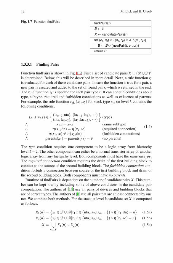
Fig. 1.7 Function findPairs findPairs(t)
B ← ∅X ← candidatePairs(t)
for (c1, c2) ∈ {(c1, c2) ∈ X |rt (c1, c2)}B ← B ∪ {newPair(t , c1, c2)}
return B
1.3.3.1 Finding Pairs
Function findPairs is shown in Fig. 1.7. First a set of candidate pairs X ⊆ (B∪D)2
is determined. Below, this will be described in more detail. Next, a rule function rt
is evaluated for each of these candidate pairs. In case the function is true for a pair, anew pair is created and added to the set of found pairs, which is returned in the end.The rule function rt is specific for each pair type t. It can contain conditions abouttype, subtype, required and forbidden connections as well as existence of parents.For example, the rule function rstk
(x1,x2) for stack type stk on level k contains thefollowing conditions,
(x1.t,x2.t) ∈{(lak−2,nta), (lak−2, la2), · · ·)(nta, lak−2), (la2, lak−2), · · ·)
}(type)
∧ x1.s = x2.s (same subtype)∧ η(x1,dn) = η(x2,sc) (required connection)∧ η(x1,sc) �= η(x2,dn) (forbidden connections)∧ parents(x1) = parents(x2) = /0 (no parents)
(1.4)
The type condition requires one component to be a logic array from hierarchylevel k− 2. The other component can either be a normal transistor array or anotherlogic array from any hierarchy level. Both components must have the same subtype.The required connection condition requires the drain of the first building block toconnect to the source of the second building block. The forbidden connection con-dition forbids a connection between source of the first building block and drain ofthe second building block. Both components must have no parents.
Runtime of findPairs is dependent on the number of candidate pairs X . This num-ber can be kept low by including some of above conditions in the candidate paircomputation. The authors of [14] use all pairs of devices and building blocks thatare of correct types. The authors of [8] use all pairs that are at least connected by onenet. We combine both methods. For the stack at level k candidate set X is computedas follows,
X1(n) ={
x1 ∈ D ∪B|x1.t ∈ {nta, la2, la4, . . .})∧η(x1,dn) = n} (1.5a)
X2(n) ={
x2 ∈ D ∪B|x2.t ∈ {nta, la2, la4, . . .})∧η(x2,sc) = n} (1.5b)
X =⋃
n∈N
X1(n)×X2(n) (1.5c)

1 Towards Automatic Structural Analysis of Mixed-Signal Circuits 13
findArrays(t)
B ← ∅X ← {c ∈ D ∪ B|rt (c)}K ← ∪x∈X{kt (c)}for κ ∈ K
Xκ ← {x ∈ X |kt (x) = κ}|Xκ| ≥ t .m
true falseB ← B ∪ {newArray(t , Xκ)}
return B
findChains(t)
B ← ∅X ← {c ∈ D ∪ B|rt (c)}y0 ∈ {x ∈ X |γ−
X (x) = 1}y ← unbranchedChain(x0, X )
B ← B ∪ {newChain(t , y )}return B
Fig. 1.8 Function findArrays Fig. 1.9 Function findChains
Functions X1(n) and X2(n) return candidates for the first and second componentfor a specific net n ∈ N , respectively. Pairs are then computed for each net n ∈ Nby evaluating X1(n) and X2(n). The resulting set X only contains pairs where theconnection condition and parts of the type condition are fulfilled.
1.3.3.2 Finding Arrays
The algorithm to find arrays is depicted in Fig. 1.8. First, the algorithm creates aset X of candidate children by evaluating a rule function rt , which is specific foreach array type t. It can consist of conditions about type, subtype, connectivity andexistance of parents. The rule function rdta(x) for a diode transistor array containsthe following conditions:
x.t = trans︸ ︷︷ ︸(type)
∧ η(x,gt) = η(x,dn)︸ ︷︷ ︸(required connection)
∧ η(x,dn) �= η(x,sc)︸ ︷︷ ︸(forbidden connection)
(1.6)
It enforces type transistor and a gate drain connection. It forbids a connection be-tween drain and source. The key function kt maps each component in X to a tuple ofnets, such that components connected in parallel get the same key. The key functionkdta for a diode transistor array is,
kdta(x) = (η(x,dn),η(x,sc)). (1.7)
This means, for a diode transistor array all transistors are grouped together thatconnect to the same net at their drain pins and their source pins. If more than aminimum number t.m building blocks are connected in parallel then a new arrayis created. For the diode transistor array dta.m = 1, i.e., an array is always created.Finally, the set B of new arrays is returned.

14 M. Eick and H. Graeb
1.3.3.3 Finding Chains
Function findChains is shown in Fig. 1.9. First, the algorithm computes a set Xof candidate children using a rule function rt , which is specific for each chaintype t. It can use the conditions described for arrays. All candidate children must bepairs. The rule function rsck(x) for a stack chain on level k contains the followingconditions:
x.t = stk−1 . (1.8)
It requires x to be a stack on level k− 1.Next, all tuples y = (y0,y1, . . .ylast) with the following properties are found:
• γ−(y0) = |{x ∈ X |x.c2 = y0.c1}| �= 1, i.e., more than one or no candidate in Xshare the second child with y0.
• yi.c2 = yi+1.c1 for yi �= ylast, i.e., the second child of each building block yi isthe first child of the next building block yi+1.
• |{x ∈ X |x.c1 = ylast.c2}| �= 1, i.e., the chain can not be continued beyond ylast.
Finally, a new chain is created for each y and returned in B.
1.3.3.4 Discussion
The analog building block recognition described in [14] is included in this algo-rithm. It corresponds to the analog part of the library in Fig. 1.3 and the dominancegraph in Fig. 1.5. The algorithm corresponds to the algorithm of Fig. 1.6 whenall building blocks are pairs. Consequently, the results obtained for the algorithmof [14] can be transfered to the new algorithm.
The authors of [1] suggested to recognize simple current mirrors and level-shifters by recognizing diode connected transistors first. Application of the prin-ciple from [1] to the library from [14] resulted in the new hierarchy level 1 shownin Fig. 1.3. This has the advantage of faster recognition of pairs because less rulesmust be evaluated.
1.4 Structural Signal Flow Analysis
After applying the building block algorithm from the previous section to a circuit,basic building blocks such as pass-gates or simple current mirrors are known. Fig-ure 1.10 illustrates this for a latch from [19]. It consists of logic gates lg1
2 to lg32
as well as pass–gates pg12 and pg2
2. This information is now used to generate theEnhanced Structural Signal Flow Graph [6] (ESFG) of the circuit, which combinesqualitative behavioral and structural information. This graph is then used to assigna direction to each pass–gate, partition the circuit into an analog and digital part andto identify feedback loops.

1 Towards Automatic Structural Analysis of Mixed-Signal Circuits 15
lg32 lg2
2
lg12
pg2
pg1
D
E
Q
Q
nD
DnQ
nQ
Q
Q
nE
Ena nb
e10
e2
e4
e20
e5
e11e14
e13
e12
e21
e22
e23
e24
Fig. 1.10 Latch [19] with recognizedbuilding blocks
Fig. 1.11 Generated ESFG
1.4.1 Generation
An ESFG [6] is a directed graph. The nodes of the graph are formed by the netsof the circuit. An edge models a qualitative influence from one net to another. Anedge from net ni to n j means that a change of a branch current or voltage of ni
causes a change of a branch current or voltage of n j. The relation between edges andthe recognized building blocks is modeled by some edge attributes. Only top–levelbuilding blocks without parents are considered. The ESFG is generated as follows.
• For a logic gate edges from each input to the output are generated.• A pass–gate generates an undirected edge from drain to source. Directed edges
are generated from both gates to drain and source. These edges are called controledges.
• For analog building blocks the generation is described in [6, 7]. For example, forcurrent mirrors one edge from the input to the output is generated.
• For each port of the circuit a port node is generated and connected to the corre-sponding net.
For the latch example this is illustrated by Fig. 1.11. Logic gates lg12 to lg3
2 arerepresented by edges e1 to e3. Pass–gate pg1 is represented by undirected edge e10
and control edges e11 to e14. Pass–gate pg2 is represented by edges e20 to e24. Circuitports E , D, Q, Q are represented by port nodes.
1.4.2 Assignment of Pass–Gate Directions
After the generation step, pass–gates are represented as undirected edges, e.g.,edge e10 in Fig. 1.11. In reality pass–gates are only used in one direction. The prob-lem is related to the problem of determining the signal flow direction of transistorsin switch–level simulation [2]. However, only a small part of the ESFG edges is

16 M. Eick and H. Graeb
undirected in our case, which allows to used a different approach which is describedin the following.
Assume e is an undirected edge connecting nodes ν and μ . It is replaced by adirected edge from μ to ν , if the following conditions hold simultaneously.
• An output node is reachable from ν without traversing e, and,• no edge representing a logic gate ends at ν .
Simultaneously with the assignment, edges pointing from the control inputs of thepass–gate to μ are removed.
For the undirected edge e10, connecting nD and nQ in the example of Fig. 1.11,output node nQ is reachable from nQ but not from nD without traversing edge e10.Consequently the edge points from nD to nQ. The undirected edge e20 between n2
and nQ is found to point from n2 to nQ. The control edges are removed accord-ingly (Fig. 1.12).
In some cases, it is not possible to assign directions to all pass–gates at once.In these cases above conditions are repeatedly evaluated for all pass–gates withoutassigned direction. In each iteration at least one pass–gate direction is assigned. Thealgorithm needs npg iterations at maximum, where npg is the number of pass–gates.
The computation of the logic functions (see Section 1.5.1) for building blockscan be done before this step. In this case, it can be checked whether the output of alogic gate can be in high impedance state.
1.4.3 Analog / Digital Partitioning
For further processing, the ESFG must be partitioned into an analog and digitalpart. Therefore a signal type is assigned to each node. This signal type can be eitherunknown, analog or digital. The signal type for each node is determined based onthe edges of the graph and the building blocks they represent. For each buildingblock type a specific set of conditions for the connected nodes exists. For example,input and output of a current mirror must be of type analog. In addition, the user canspecify the signal type of inputs and outputs of the circuit. Overall, we get a set ofconditions forming a constraint satisfaction problem which is solved by a constraintprogramming method, e.g., [17].
nD nQ
nQ
nE na nbQ
Q
E
D
nD nQ
nQ
nE na
nb
n′Q
Q
Q
E
D
Q′
Fig. 1.12 ESFG after assignment of pass-gate directions
Fig. 1.13 Temporal ESFG
1 Towards Automatic Structural Analysis of Mixed-Signal Circuits 17
In some cases, this leads to conflicting requirements for a node, i.e., it must beanalog and digital at the same time. This happens in case an analog building blockwas wrongfully recognized in the digital part or vice versa. Such conflicts are re-solved by back–annotating the signal type to the nets of the circuit. Next, the build-ing block recognition is rerun using additional rules for the signal types at the pinsof a building block.
For a pure analog or digital circuit this step has no effect. Therefore the ESFG inFig. 1.12 does not change.
1.4.4 Transformation to Temporal ESFG
In case of sequential circuits such as latches, the ESFG contains feedback loops. Inorder to compute the logic function of such circuits, a temporal ESFG is introduced,which is an acyclic ESFG and adds a time concept.
Definition 5 (Temporal ESFG). A temporal ESFG is an acyclic ESFG. It refers to avirtual normalized clock with clock period 1 that is at least twice thereal clock frequency, i.e., the real clock can be sampled. Each node gets an addi-tional clock cycle attribute, indicating if the node belongs to the current or a previousclock cycle.
The transformation from the ESFG to the temporal ESFG is described in the follow-ing. All loops of the ESFG are computed by finding strongly connected componentsin the graph. All nodes, where an edge to a node outside the loop starts, are calledoutput nodes of the loop. All nodes, where an edge from a node outside the loopends, are called input nodes of the loop. The feedback path of a loop is the pathfrom an output node to an input node that does not contain any other output or inputnode of the loop. Some node ns of this path, which is not an input node of the loop,is then selected as node to represent the state of the loop. This node is split up intotwo nodes ns and n′s, which represent the state at the current and previous time step,respectively. All edges going from ns to a node inside the loop are assigned to n′s.All other edges are assigned to ns. In addition, an output port node corresponding tons and an input port node corresponding to n′s is created.
Figure 1.13 illustrates this for the example. The ESFG (Fig. 1.12) contains a loopconsisting of nQ, nQ and nb. Node nQ is an input node of the loop and nodes nQ, nQare output nodes. The feedback path is nQ,nb,nQ. Node nQ is split up into node nQ
and n′Q
. Input port Q′is created. The resulting temporal ESFG is shown in Fig. 1.13.
1.5 Logic Function Extraction
Based on the temporal ESFG the logic function of the circuit can now be computed.This is done in two steps. First, the logic function for all recognized building blocksis computed. Afterwards, the logic function for the complete circuit is determined.

18 M. Eick and H. Graeb
Unless denoted otherwise, a four valued logic [4] with 0, 1, Z (high impedance),U (unknown) is used in the following. All logic functions are represented usingROBDDs [3].
1.5.1 Computation of Logic Function for Building Blocks
In this step, the logic function of single logic gates is determined. For CMOS cir-cuits this requires in general to evaluate the serial and parallel connections of thepull–up and pull–down network [19]. Algorithmic implementations can be foundin, e.g., [4, 5, 9, 11, 20]. Our approach builds on the hierarchical recognition resultcomputed by the algorithm presented in Sec. 1.3.
Table 1.1 lists the logic function associated with each building block from thelibrary for digital circuits. It uses the operators ⊕ and �, which are defined asfollows.
a⊕ b :⇔⎧⎨⎩
a (a = b)∨ (b = Z)b a = ZU otherwise
a � b :⇔⎧⎨⎩
a b =Ub a =U
a⊕ b otherwise(1.9)
The operator ⊕ is the “merge” operator from [4]. The result is a defined logic state,i.e., zero or one, if a and b have the same value or one is high impedance. If bothare high impedance the result is “Z”, otherwise the result state is undefined. Theoperator � considers in addition, that undefined states can be canceled out in caseof parallel connections, i.e., the result is a defined logic state in case a or b is 0 or 1and the other one is undefined.
An NMOS transistor for example shows a logic “0” at the drain pin if the gate isat logic “1” (i.e., vdd) and source is at logic “0”. The drain pin is at high impedancestate if the transistor is off. This is the case for “0” at the gate or “Z” at the sourcepin. In all other cases the output is unknown (Table 1.1). The logic function for aPMOS transistor is found analogously.
The logic function at the drain pin of a stack chain is formed out of the logicfunctions f1 to fn of its children. The gate inputs of these children are described byvectors g1 to gn. The overall logic function is the logic function fn with fn−1 substi-tuted for the source variable. These substitutions are continued until f1 is reached.
The logic function at the output o of a logic gate are the logic functions of the p–and the n–block combined by the ⊕ operator. This includes that the output becomeshigh–impedance in case no block is on or unknown in case both blocks are on at thesame time.
The logic function of a logic array is the logic functions f1 to fn of the childrencombined by the � operator. The logic function at the output o of a pass–gate isequal to the input i in case the pass–gate is on, otherwise it is “Z”.

1 Towards Automatic Structural Analysis of Mixed-Signal Circuits 19
Table 1.1 Logic functions for digital building blocks
n–transistor d
sg
d = fn-t(g,s) =
⎧⎨⎩
0 (g = 1)∧ (s = 0)Z (g = 0)∨ (s = Z)U otherwise
p–transistor d
sg
d = fp-t(g,s) =
⎧⎨⎩
1 (g = 0)∧ (s = 1)Z (g = 1)∨ (s = Z)U otherwise
stack chain
sf1
f2
fnd
g1
g2
gn
d = fsc([g1g2 · · ·gn],s)= fn(gn, fn−1(gn−1, · · · f1(g1,s) · · ·))
logic gate
sn
fn
fpsp
gn
gpo
o= f ([gpgn],sp,sn) = fn(gn,sn)⊕ fp(gp,sp)
logic array
sf1 f2 fn
dg1 g2 gn
d = fla([g1g2 · · ·gn],s)= f1(g1,s)� f2(g2,s)� · · · � fn(gn,s)
pass–gateo
an
i
ap
o = f (i,ap,an) =
⎧⎨⎩
i (an = 1)∧ (ap = 0)Z (an = 0)∧ (ap = 1)U otherwise
This is illustrated by the example shown in Fig. 1.14. The logic function for thecomplete gate,
fNAND([a b]) = fN2(a, fN1 (b,0))︸ ︷︷ ︸fN([a,b],0)
⊕( fP1(a,1)� fP2(b,1))
︸ ︷︷ ︸fP([a,b],1)
(1.10)
is formed by the logic function fP of the logic array consisting of P1 and P2 as wellas the logic function fN of the stack chain consisting of N1 and N2. Logic function fP
is formed by the logic functions of P1 and P2 and logic function fN is formed by thelogic functions of N1 and N2, yielding
fN([a b],0) =
⎧⎨⎩
0 (a = 1)∧ (b = 1)Z (a = 0)∨ (b = 0)U otherwise
fP([a b],1) =
⎧⎨⎩
1 (a = 0)∨ (b = 0)Z (a = 1)∧ (b = 1)U otherwise
.
(1.11)
Logic function fN represents the output of the pull–down network, which is the drainof N1. It is vss (“0”) in case both inputs are one, if both inputs are zero it is high-impedance. In case one input is high–impedance or unknown fN is unknown. Logicfunction fP represents the output of the pull–up network at point x1 in Fig. 1.14.
This results in the following logic function for the complete gate,
fNAND([a b]) =
⎧⎨⎩
0 (a = 1)∧ (b = 1)1 (a = 0)∨ (b = 0)
U otherwise, (1.12)

20 M. Eick and H. Graeb
which is the logic function of a NAND gate. The unknown case occurs if one of theinputs is in unknown or high–impedance state. Since the NAND gate is no tristategate, the overall logic function does not include a high–impedance case.
1.5.2 Computation of Overall Logic Function
The overall logic function is computed by assigning logic variables to each node.We use a temporal logic, i.e., the logic variables refer to different time steps. Next,the temporal ESFG is traversed in topological order, i.e., each node in the graph isvisited after all nodes it depends on. During this traversal, the logic functions aresubstituted into each other. In case two building blocks (e.g., pass gates) have out-puts o1, o2 on the same node, the logic function for the node is calculated as o1 ⊕ o2.It is assumed, that the inputs of the circuit are in a defined logic state, i.e., they arenot “U” or “Z”.
For the example circuit from Fig. 1.10 and the temporal ESFG from Fig. 1.13the assigned logic variables are shown in Fig. 1.15. Logic variables a(t), b(t), D(t),E(t), Q(t) and Q(t) refer to the current time step. Logic variable Q(t − 1) refers tothe previous time step. It holds.
a(t) =
{0 E(t) = 11 E(t) = 0
b(t) =
⎧⎨⎩
0 Q(t − 1) = 11 Q(t − 1) = 0
U otherwise(1.13)
Q(t) =
⎧⎨⎩
0[(E(t) = 1)∧ (D(t) = 0)
]∨ [(E(t) = 0)∧ (Q(t − 1) = 1)]
1[(E(t) = 1)∧ (D(t) = 1)
]∨ [(E(t) = 0)∧ (Q(t − 1) = 0)]
U otherwise(1.14)
Q(t) =
⎧⎨⎩
0[(E(t) = 1)∧ (D(t) = 1)
]∨ [(E(t) = 0)∧ (Q(t − 1) = 0)]
1[(E(t) = 1)∧ (D(t) = 0)
]∨ [(E(t) = 0)∧ (Q(t − 1) = 1)]
U otherwise(1.15)
Logic function a(t) can only become “0” or “1” because input E(t) is assumed tobe in a defined logic state. No such assumption is made for Q(t −1). Consequently,b(t) can become unknown in case Q(t − 1) is unknown or high-impedance. Overall
oa
b
P2P1
N1
N2
x1
D(t)D(t)
Q(t)
Q(t)
Q(t)
Q(t)
E(t)E(t)
a(t)b(t)
Q(t − 1)Q(t − 1)
Fig. 1.14 NAND gate Fig. 1.15 ESFG with assigned logic vari-ables

1 Towards Automatic Structural Analysis of Mixed-Signal Circuits 21
Table 1.2 Recognition results for different standard cell libraries
Library No. Cells Analysis Time CoverageLib 1 32 1 sec. 100.0%Lib 2 134 4 sec. 100.0%Lib 3 – Tech 1 ∼ 600 18 sec. 97.6%Lib 3 – Tech 2 ∼ 550 13 sec. 99.6%Lib 3 – Tech 3 ∼ 700 27 sec. 99.1%Lib 4 ∼ 850 37 sec. 95.2%
logic function Q(t) is input D(t) in case E(t) is set otherwise it is the inversion ofQ(t − 1). Logic function Q(t) is the inversion of Q(t). This corresponds to a latch.
1.6 Application Examples
In the following application to digital standard cell libraries and mixed-signal cir-cuits is discussed including experimental results.
1.6.1 Description Generation for Digital Standard Cell Libraries
The approach is used to automatically generate a library description for digital stan-dard cell libraries. The description includes a decomposition into pass–gates andlogic gates, the ESFG, the logic function of the standard cell and a table listingpossible single input switching events together with the possible values at the otherinputs and the resulting output behavior. These events are a necessary input for au-tomatic timing characterization of digital standard cell libraries. The decompositioninto logic gates and pass–gates corresponds to a decomposition of multi–stage gatesinto single–stage gates. This is a required input for the current–source modelingapproach of [10] and the aging analysis approach of [12].
In the experiment, the building block recognition with the digital part of the li-brary is used as well as the structural signal flow analysis and the logic functionextraction. Additional post–processing is used to generate the table of all possiblesingle input switching events.
We performed this analysis for 4 different standard cell libraries (Table 1.2). Li-brary 1 is the standard cell library included in the FreePDK presented in [18]. Li-brary 2 is the Nangate open cell library. Library 3 is an industrial standard celllibrary which was available for three different technology nodes. Library 4 is anindustrial standard cell library, too.
Table 1.2 shows that these libraries contained between 30 and 850 cells. In allcases the analysis for the complete library took less than 1 minute. All runtimes

22 M. Eick and H. Graeb
were normalized to an Intel R© Xeon R© 2.33 GHz computer with 4 GB RAM runningUbuntu and using 4 of 8 cores in parallel.
Column four of Table 1.2 gives the recognition coverage of the presented method.For libraries 1 and 2 all cells were recognized correctly. For libraries 3 and 4, thebuilding block analysis was not able to fully decompose all cells into pass–gates andlogic gates. Typically, these cells were not designed according to standard CMOSprinciples. However, these cells can be included by extending the library accord-ingly. Overall, more than 95% of all cells were correctly recognized for the indus-trial libraries.
1.6.2 Structural Analysis of Mixed-Signal Circuits
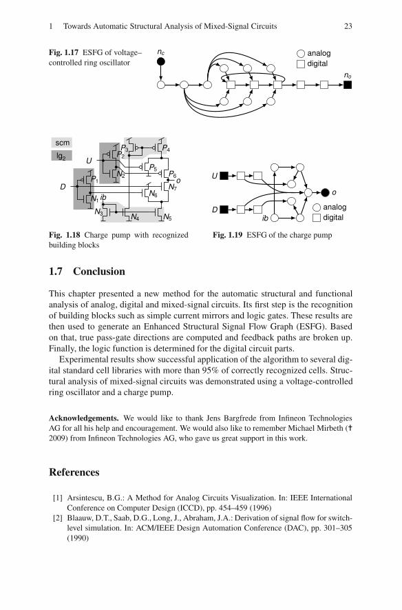
The new mixed–signal capabilities of the structural analysis were evaluated using avoltage–controlled ring oscillator (Fig. 1.16) and a charge–pump (Fig. 1.18).
The voltage–controlled ring oscillator generates a digital clock signal. The fre-quency of the clock signal can be adjusted by the analog control voltage applied atinput c. The building block recognition computed 4 NMOS simple current mirrors,3 PMOS simple current mirrors and 5 logic gates on level 2, i.e., inverter. It is notpossible to get the correct recognition result by computing analog and digital build-ing blocks independently: A logic gate on level 4 consisting of N3, N4, P3, P4 wouldbe found, which would contradict the current mirrors formed by N1,N4 and P1,P2.
Fig. 1.17 shows the corresponding ESFG of the voltage–controlled ring oscilla-tor. The partitioning into analog and digital part is symbolized by the node shape.The analog control circuitry as well as the digital feedback loop are clearly visible.
The charge pump shown in Fig. 1.18 is based on [15]. The output is usuallyconnected to the loop filter of a PLL. Digital inputs D and U control the directionof the output current. The building block recognition computed 2 NMOS simplecurrent mirrors, a PMOS simple current mirror and two logic gates. Transistors N6
and N7 as well as P5 and P6 would match a differential pair. These differential pairswere dropped because they connect to digital inputs D and U . Transistors N7 and P6
would form a logic gate, which was dropped because output o is specified as analog.The corresponding ESFG is shown in Fig. 1.19.
Fig. 1.16 Voltage–controlled ring oscillatorwith recognized buildingblocks
lg2scm
o
cP3
P4
N3
N4
P5
P6
N5
N6
P7
P8
N7
N8
P9
N9
P10
N10
P2P1
N2N1
1 Towards Automatic Structural Analysis of Mixed-Signal Circuits 23
Fig. 1.17 ESFG of voltage–controlled ring oscillator
nc
no
digitalanalog
lg2
scm
oP1
ib
U
DN1
P2
N2
N4 N5
N6N7
N3
P4
P5P6
P3
ib
o
D
U
digitalanalog
Fig. 1.18 Charge pump with recognizedbuilding blocks
Fig. 1.19 ESFG of the charge pump
1.7 Conclusion
This chapter presented a new method for the automatic structural and functionalanalysis of analog, digital and mixed-signal circuits. Its first step is the recognitionof building blocks such as simple current mirrors and logic gates. These results arethen used to generate an Enhanced Structural Signal Flow Graph (ESFG). Basedon that, true pass-gate directions are computed and feedback paths are broken up.Finally, the logic function is determined for the digital circuit parts.
Experimental results show successful application of the algorithm to several dig-ital standard cell libraries with more than 95% of correctly recognized cells. Struc-tural analysis of mixed-signal circuits was demonstrated using a voltage-controlledring oscillator and a charge pump.
Acknowledgements. We would like to thank Jens Bargfrede from Infineon TechnologiesAG for all his help and encouragement. We would also like to remember Michael Mirbeth (�2009) from Infineon Technologies AG, who gave us great support in this work.
References
[1] Arsintescu, B.G.: A Method for Analog Circuits Visualization. In: IEEE InternationalConference on Computer Design (ICCD), pp. 454–459 (1996)
[2] Blaauw, D.T., Saab, D.G., Long, J., Abraham, J.A.: Derivation of signal flow for switch-level simulation. In: ACM/IEEE Design Automation Conference (DAC), pp. 301–305(1990)

24 M. Eick and H. Graeb
[3] Bryant, R.E.: Graph-Based Algorithms for Boolean Function Manipulation. IEEETransactions on Computers 35(8), 677–691 (1986)
[4] Bryant, R.E.: Extraction of gate level models from transistor circuits by four-valuedsymbolic analysis. In: IEEE International Conference on Computer-Aided Design, IC-CAD 1991. Digest of Technical Papers, pp. 350–353 (1991)
[5] Dagenais, M.R.: Efficient algorithmic decomposition of transistor groups into series,bridge, and parallel combinations. IEEE Transactions on Computer-Aided Design ofIntegrated Circuits and Systems 38(6), 569–581 (1991)
[6] Eick, M., Graeb, H.: MARS: Matching-driven Analog Sizing. IEEE Transactions onComputer-Aided Design of Integrated Circuits and Systems (2012)
[7] Eick, M., Strasser, M., Lu, K., Schlichtmann, U., Graeb, H.: Comprehensive Generationof Hierarchical Placement Rules for Analog Integrated Circuits. IEEE Transactions onComputer-Aided Design of Integrated Circuits and Systems 30(2), 180–193 (2011)
[8] Graeb, H., Zizala, S., Eckmueller, J., Antreich, K.: The Sizing Rules Method for AnalogIntegrated Circuit Design. In: IEEE/ACM International Conference on Computer-AidedDesign (ICCAD), pp. 343–349 (2001)
[9] Kim, W., Shin, H.: Hierarchical LVS based on hierarchy rebuilding, pp. 379–384(1998)
[10] Knoth, C., Kleeberger, V.B., Nordholz, P., Schlichtmann, U.: Fast and Waveform In-dependent Characterization of Current Source Models. In: IEEE/VIUF InternationalWorkshop on Behavioral Modeling and Simulation (BMAS), pp. 90–95 (2009)
[11] Lester, A., Sabet, P.B., Greiner, A.: YAGLE, a second generation functional abstractorfor CMOS VLSI circuits. In: Proceedings of the Tenth International Conference onMicroelectronics, ICM 1998, pp. 265–268 (1998)
[12] Lorenz, D., Barke, M., Schlichtmann, U.: Aging analysis at gate and macro cell level.In: IEEE/ACM International Conference on Computer-Aided Design (ICCAD), pp. 77–84 (2010)
[13] Lullau, F., Hoepken, T., Barke, E.: A Technology Independent Block Extraction Algo-rithm. In: ACM/IEEE Design Automation Conference (DAC), pp. 610–615 (1984)
[14] Massier, T., Graeb, H., Schlichtmann, U.: The Sizing Rules Method for CMOS andBipolar Analog Integrated Circuit Synthesis. IEEE Transactions on Computer-AidedDesign of Integrated Circuits and Systems 27(12), 2209–2222 (2008)
[15] Rhee, W.: Design of high-performance CMOS charge pumps in phase-locked loops. In:IEEE International Symposium on Circuits and Systems (ISCAS), vol. 2, pp. 545–548(1999)
[16] Rubanov, N.: A High-Performance Subcircuit Recognition Method Based on the Non-linear Graph Optimization. IEEE Transactions on Computer-Aided Design of IntegratedCircuits and Systems 25(11), 2353–2363 (2006)
[17] Schulte, C., Tack, G., Lagerkvist, M.Z.: Modeling and Programming with Gecode(2010), http://www.gecode.org/doc/3.4.0/MPG.pdf
[18] Stine, J., Castellanos, I., Wood, M., Henson, J., Love, F., Davis, W., Franzon, P., Bucher,M., Basavarajaiah, S., Oh, J., Jenkal, R.: FreePDK: An Open-Source Variation-AwareDesign Kit. In: IEEE International Conference on Microelectronic Systems Education,MSE 2007, pp. 173–174 (2007)
[19] Weste, N.H.E., Harris, D.: CMOS VLSI Design - A Circuits and Systems Perspective.Pearson Education, Inc. (2005)

1 Towards Automatic Structural Analysis of Mixed-Signal Circuits 25
[20] Yang, L., Shi, C.J.R.: FROSTY: A Fast Hierarchy Extractor for Industrial CMOS Cir-cuits. In: IEEE/ACM International Conference on Computer-Aided Design (ICCAD),pp. 741–746 (2003)
[21] Zhang, N., Wunsch II, D.C.: Speeding up VLSI Layout Verification Using FuzzyAttributed Graphs Approach. IEEE Transactions on Fuzzy Systems 14(6), 728–737(2006)
[22] Zhang, N., Wunsch II, D.C., Harary, F.: The subcircuit extraction problem. In: Pro-ceeding of IEEE International Behavioral Modeling and Simulation Workshop 2005,vol. 22(3), pp. 22–25 (2003)

M. Fakhfakh et al. (Eds.): Analog/RF & Mixed-Signal Circuit Sys. Design, LNEE 233, pp. 27–52. DOI: 10.1007/978-3-642-36329-0_2 © Springer-Verlag Berlin Heidelberg 2013
Chapter 2 Efficient Synthesis Methods for High-Frequency Integrated Passive Components and Amplifiers
Bo Liu*and Georges Gielen
Abstract. Existing design automation methods for RF ICs and microwave passive components often rely on parasitic-aware lumped equivalent circuit models. That framework is difficult to apply to synthesis tasks at high frequencies (e.g. 40GHz and above) due to the distributed effect. When directly embedding the computa-tionally expensive electromagnetic (EM) simulations in the optimization loop, a too long synthesis time results. This chapter presents a new method for high-frequency integrated passive component synthesis, called Memetic Machine Learning-based Differential Evolution (MMLDE), and the first method for mm-wave integrated circuit synthesis, called Efficient Machine Learning-based Differential Evolution (EMLDE), both addressing the problem of obtaining highly optimized design solutions in a very practical time. The common idea of these two methods is the on-line surrogate model assisted evolutionary algorithm (SAEA), where a computationally cheap surrogate model is constructed adaptively in the optimization process to replace expensive EM simulations. The differences be-tween the two algorithms are that a memetic SAEA is built to enhance the optimi-zation ability and efficiency in MMLDE, while a decomposition method is used to address the “curse of dimensionality” of SAEA in EMLDE. Experimental results show the effectiveness and the high efficiency obtainable with MMLDE and EMLDE.
2.1 Introduction
In recent years, design methodologies for high-frequency and mm-wave circuits have attracted a lot of attention. In particular, research and applications on RF building blocks for 40 GHz to 120 GHz and beyond are increasing drastically [1]. Existing RF IC synthesis methodologies, however, focus on low-GHz cases [2,3]. Even till now, the synthesis methodologies for mm-wave frequencies are still
Bo Liu · Georges Gielen ESAT-MICAS, KU Leuven, Kasteelpark Arenberg 10, B3001, Leuven, Belgium e-mail: {Bo.Liu,Georges.Gielen}@esat.kuleuven.be, [email protected]

28 B. Liu and G. Gielen
lacking. Designers rely on experience and simulation verifications when designing these circuits. Due to the high-performance and tightening time-to-market re-quirements, this “experience and trial” method or local optimization is often not good enough.
The reason why existing synthesis methods cannot be extended to mm-wave frequencies is that they all rely on parasitic-aware equivalent circuit models for passive components [2,3,4]. Due to the distributed effects, however, an accurate equivalent circuit model is difficult to find at mm-wave frequencies. The solution is to include electromagnetic (EM) simulation based on the actual layout structure in the optimization loop. However, EM simulation is computationally very expen-sive. When combining it directly with techniques like evolutionary computation (EC) [5], like at low frequencies, high-quality solutions can be obtained, but the time consumption is extremely large. For example, the synthesis of a transformer typically needs more than 20 hours, and the synthesis of a linear amplifier needs about 10 days. This is not practical for real-world applications.
In this chapter, efficient synthesis method for mm-wave-frequency passive components and linear amplifiers will be introduced. The Memetic Machine Learning-based Differential Evolution (MMLDE) method [6] for the synthesis of integrated passive components will briefly be introduced first. The key idea of MMLDE is the on-line surrogate model-based memetic evolutionary optimization mechanism, whose training data are generated adaptively in the optimization process. By using the Gaussian Process with the expected improvement prescreen-ing method and an artificial neural network with the prediction value in the pro-posed search mechanism, surrogate models are constructed on-line to predict the performances. Hence, the computationally expensive EM simulations are only used in the necessary part of the design space, which is guided by the prediction and prescreening methods. Compared with directly using EC algorithms, MMLDE can obtain comparable results, and has approximately a tenfold improvement in computational efficiency. The Efficient Machine Learning-based Differential Evo-lution (EMLDE) method [7] for the synthesis of mm-wave linear amplifiers will then be elaborated next. A decomposition method is used, which separates the de-sign variables that require expensive EM simulations and the variables that only need cheap S-parameter circuit simulations. Hence, a low-dimensional but more complex expensive optimization problem is generated. By the proposed core algo-rithm integrating adaptive population generation, naive Bayes classification, Gaussian process and differential evolution, the generated low-dimensional ex-pensive optimization problem can be solved efficiently (thanks to the on-line sur-rogate model), and global search can be achieved (thanks to the evolutionary computation algorithm). A 100GHz three-stage differential amplifier in a 90nm CMOS technology is shown as an example. The power gain reaches 10dB with more than 20GHz bandwidth. The synthesis costs only 25 hours, having a compa-rable result and a 9 times speed enhancement compared with directly using the EM simulator in combination with a global optimization algorithm.
The remainder of this chapter is organized as follows. Section 2.2 reviews the existing works for RF IC synthesis, and motivates the construction of the EMLDE algorithm. Section 2.3 introduces the basic mathematical and computational

2 Efficient Synthesis Methods for High-Frequency Integrated Passive Components 29
intelligence techniques used in this chapter. Section 2.4 briefly introduces the MMLDE method as a first step for EMLDE. Section 2.5 elaborates the EMLDE method. The experimental verifications are in Section 2.6. Section 2.7 concludes the chapter.
2.2 Review of Related Works and Challenges
2.2.1 RF Integrated Circuit Synthesis
Existing RF IC design automation methods focus on low-GHz synthesis [2-4,8-14] by employing lumped equivalent circuit models for passive components (e.g. transformer, inductor). The framework of most of these methods is shown in Figure 2.1. Compared with the low-frequency analog circuit sizing flow, a key part is the generation of the parasitic-aware model of the passive components. In RF IC designs at low-GHz frequencies, a simple lumped model is often extracted to mimic the behavior of the key passive components (transformer, inductor). Regression methods are then used to fit the (calibrated) EM simulation results (S-parameters) to the parasitic-included equivalent circuit models. The generated passive component models are accurate at low-GHz frequencies and computationally efficient.
To make the parasitic-aware model reliable in providing the correct perfor-mances for different design parameters, a strictly enforced layout template is often necessary. [10,11] use the parasitic corner, rather than a strict layout template, to improve the flexibility of the generated layout for circuits below 10GHz, yielding good results. In the development of the optimization kernel, evolutionary algo-rithms (EAs) are introduced in RF IC synthesis to achieve global search, getting very good results. [14] uses Particle Swarm Optimization (PSO) and [13] intro-duces the non-dominated genetic algorithm (NSGA) to RF IC synthesis in order to achieve multi-objective optimization.
Run
ning
sim
ulat
or
Pro
vide
out
put t
o cr
eate
co
st fu
nctio
n
Fig. 2.1 Framework of parasitic-aware optimization for RF ICs (from [4])

30 B. Liu and G. Gielen
Parasitic-aware lumped equivalent circuit models for passive components that accurately match the EM simulation results are difficult to find at frequencies be-tween say 40GHz and above 100GHz due to the distributed effects at these mm-wave frequencies [6]. Hence, when employing lumped equivalent circuit models, available RF integrated circuit design automation methods are limited to low-GHz instances. Because the speed enhancement method for RF IC synthesis (using lumped models) cannot be extended to mm-wave integrated circuit synthesis, and because directly including the EM simulations in each performance evaluation is too CPU time intensive, no good efficient method for mm-wave integrated circuit synthesis exists today. The only way left to mm-wave circuit designers is the “ex-perience and simulation verification” method, which is at odds with today’s high-performance and tightening time-to-market requirements.
To summarize, the goal of this chapter is to fill the blank of efficient automated design of mm-wave-frequency integrated passive components and integrated cir-cuits (linear amplifiers as an instance), achieving good accuracy while knowing an acceptable CPU time.
2.3 Basic Computational Intelligence Techniques
The methods presented in this chapter are based on computational intelligence techniques, i.e. evolutionary computation and machine learning techniques in spe-cific. In the following, we will introduce three basic techniques: the Differential Evolution (DE) algorithm, the Gaussian Process (GP) machine learning and the Naive Bayes Classifier (NBC), which are the fundamentals for the presented algo-rithms MMLDE and EMLDE.
2.3.1 Differential Evolution
The DE algorithm [15] is selected as the search engine in MMLDE and EMLDE. The DE algorithm outperforms many other evolutionary computation (EC) algo-rithms in terms of solution quality and convergence speed. DE uses a simple diffe-rential operator to create new candidate solutions and a one-to-one competition scheme to greedily select new candidates.
The i-th candidate solution in the d-dimensional search space at generation t can be represented as
,1 ,2 ,( ) [ , , , ]i i i di t x x xx = (2.1)
At each generation t, the mutation and crossover operators are applied to the can-didate solutions, and a new population arises. Then, selection takes place, and the corresponding candidate solutions from both populations compete to comprise the next generation. The operators are now explained in detail.
For each target candidate solution, according to the mutation operator, a mutant vector is built:
,1( 1) [ ( 1), ,iiV t v t+ = + , ( 1)]i dv t + (2.2)


