32
LIGHT EMITTING DIODE – Design Principles EBB 424E Lecture 2 – LED 1 Dr Zainovia Lockman
| Date post: | 20-Dec-2015 |
| Category: |
Documents |
| View: | 223 times |
| Download: | 2 times |
LIGHT EMITTING DIODE – Design Principles
EBB 424ELecture 2 – LED 1Dr Zainovia Lockman

1907 Publication report on Curious Phenomenon
H.J. Round, Electrical World, 49, 309, 1907
On applying a potential to a crystal
of carborundum (SiC), the material gave out
a yellowish light
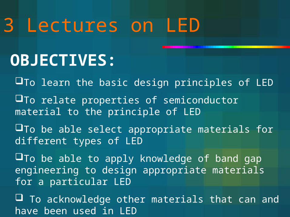
3 Lectures on LED
OBJECTIVES:To learn the basic design principles of LED
To relate properties of semiconductor material to the principle of LED
To be able select appropriate materials for different types of LED
To be able to apply knowledge of band gap engineering to design appropriate materials for a particular LED
To acknowledge other materials that can and have been used in LED
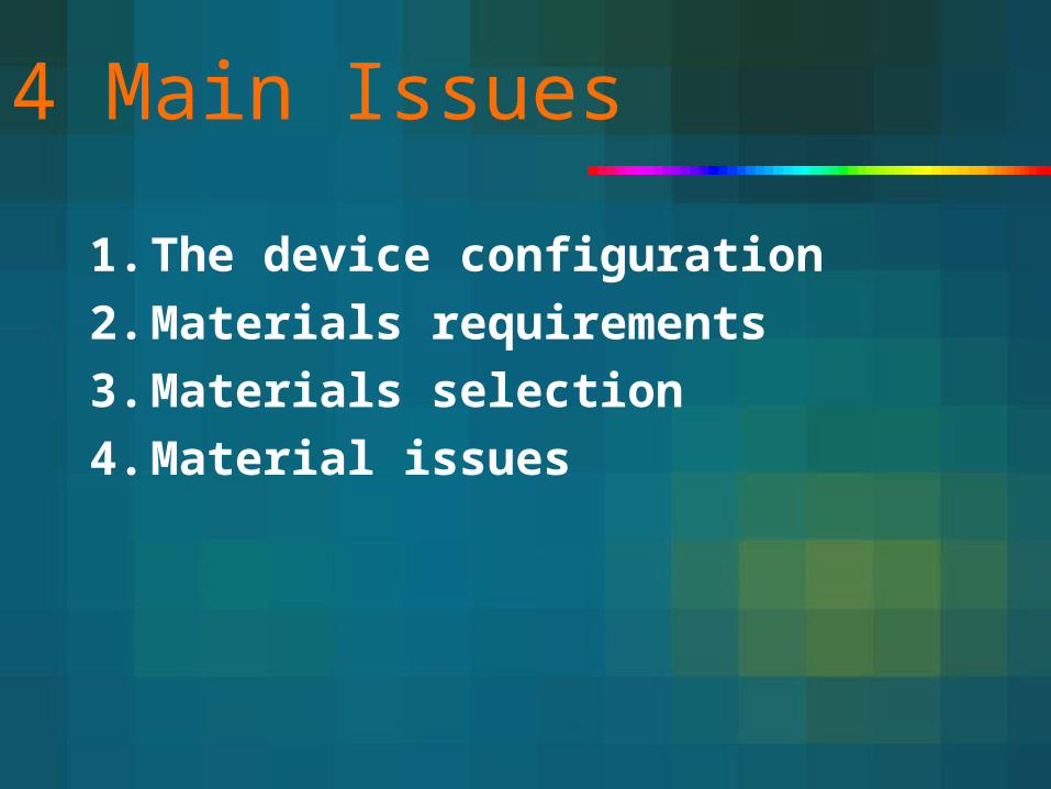
4 Main Issues
1. The device configuration
2. Materials requirements
3. Materials selection
4. Material issues

By the end of this lecture you must be able to …
Draw a typical construction of an LED. Explain your drawing. State all the issues regarding the materials
selection of an LED. State all of the possible answers regarding your
materials issues.Explain band gap engineeringExplain the isoelectronic doping in GaAsP systemState examples of materials that emit, UV, Vis, IR
lights
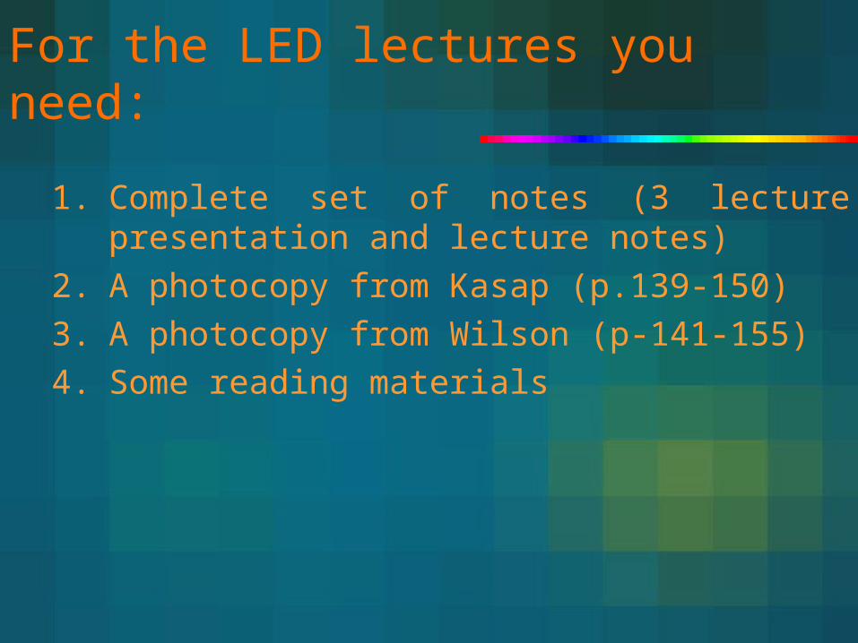
For the LED lectures you need:
1. Complete set of notes (3 lecture presentation and lecture notes)
2. A photocopy from Kasap (p.139-150)
3. A photocopy from Wilson (p-141-155)
4. Some reading materials
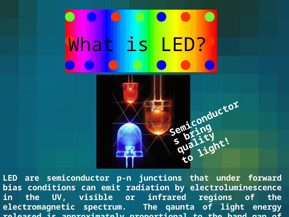
LED are semiconductor p-n junctions that under forward bias conditions can emit radiation by electroluminescence in the UV, visible or infrared regions of the electromagnetic spectrum. The qaunta of light energy released is approximately proportional to the band gap of the semiconductor.
Semiconductors
bring quality
to light!
What is LED?
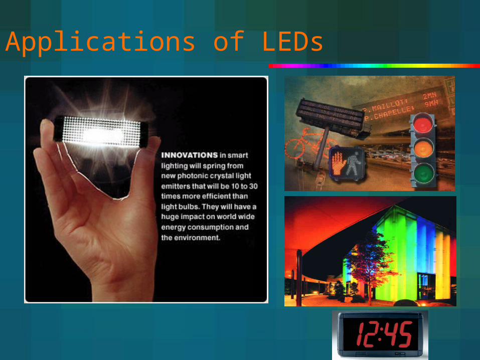
Applications of LEDs

Your fancy telephone, i-pod, palm pilot and digital camera
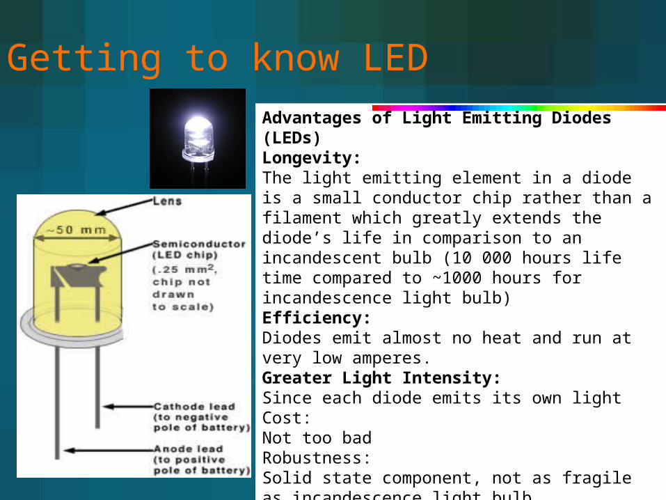
Getting to know LED
Advantages of Light Emitting Diodes (LEDs)Longevity: The light emitting element in a diode is a small conductor chip rather than a filament which greatly extends the diode’s life in comparison to an incandescent bulb (10 000 hours life time compared to ~1000 hours for incandescence light bulb)Efficiency: Diodes emit almost no heat and run at very low amperes.Greater Light Intensity: Since each diode emits its own lightCost:Not too badRobustness:Solid state component, not as fragile as incandescence light bulb

LED chip is the part that we shall deal with in this course
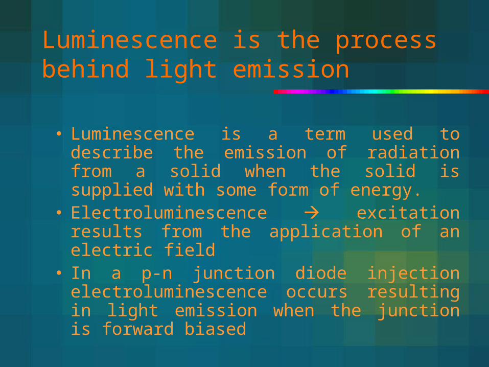
Luminescence is the process behind light emission
• Luminescence is a term used to describe the emission of radiation from a solid when the solid is supplied with some form of energy.
• Electroluminescence excitation results from the application of an electric field
• In a p-n junction diode injection electroluminescence occurs resulting in light emission when the junction is forward biased
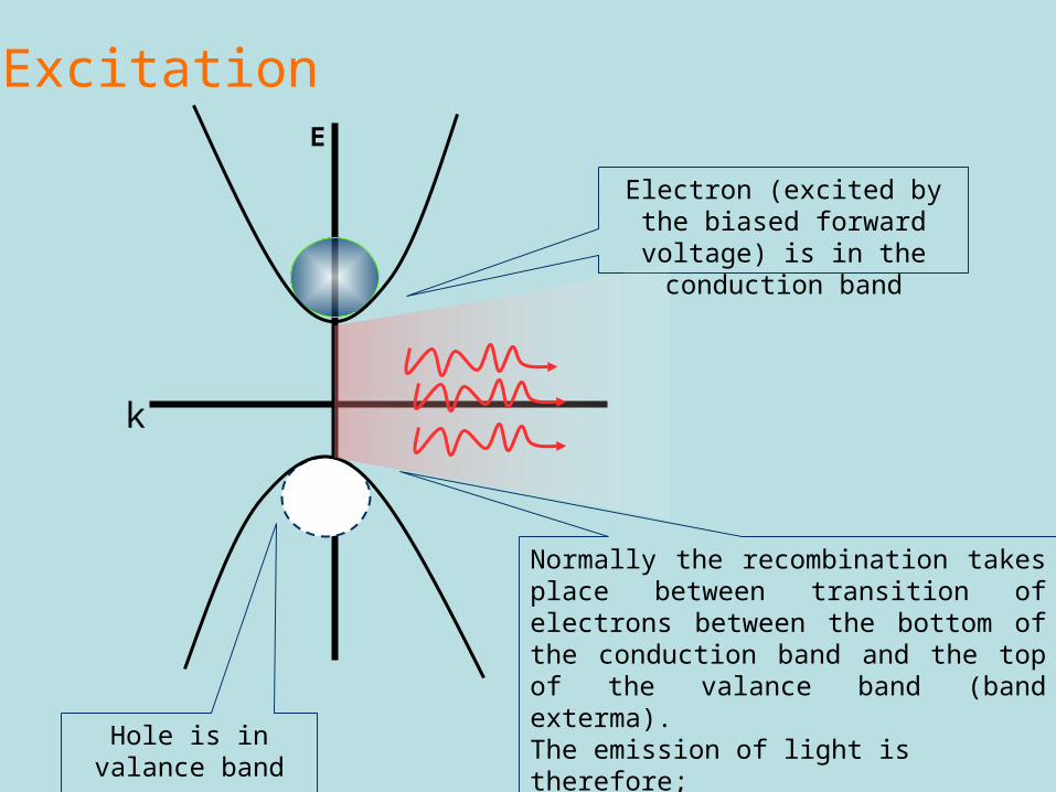
Excitation
Electron (excited by the biased forward voltage) is in the conduction
band
Hole is in valance band
Normally the recombination takes place between transition of electrons between the bottom of the conduction band and the top of the valance band (band exterma). The emission of light is therefore;hc/ = Ec-Ev = Eg(only direct band gap allows radiative transition)
E
k
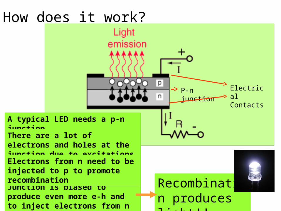
How does it work?
P-n junction
Electrical Contacts
A typical LED needs a p-n junctionA typical LED needs a p-n junction
Junction is biased to produce even more e-h and to inject electrons from n to p for recombination to happen
Junction is biased to produce even more e-h and to inject electrons from n to p for recombination to happen
There are a lot of electrons and holes at the junction due to excitationsThere are a lot of electrons and holes at the junction due to excitations
Electrons from n need to be injected to p to promote recombinationElectrons from n need to be injected to p to promote recombination
Recombination produces light!!
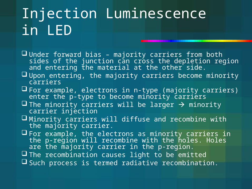
Injection Luminescence in LED
Under forward bias – majority carriers from both sides of the junction can cross the depletion region and entering the material at the other side.
Upon entering, the majority carriers become minority carriers For example, electrons in n-type (majority carriers) enter the p-type
to become minority carriers The minority carriers will be larger minority carrier injection Minority carriers will diffuse and recombine with the majority carrier. For example, the electrons as minority carriers in the p-region will
recombine with the holes. Holes are the majority carrier in the p-region.
The recombination causes light to be emitted Such process is termed radiative recombination.
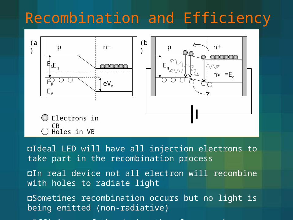
Recombination and Efficiency
eVo
Eg
p n+
h =Eg
Eg
p n+(a) (b)
Electrons in CB
Holes in VB
EC
EV
EF
◘Ideal LED will have all injection electrons to take part in the recombination process
◘In real device not all electron will recombine with holes to radiate light
◘Sometimes recombination occurs but no light is being emitted (non-radiative)
◘Efficiency of the device therefore can be described
◘Efficiency is the rate of photon emission over the rate of supply electrons
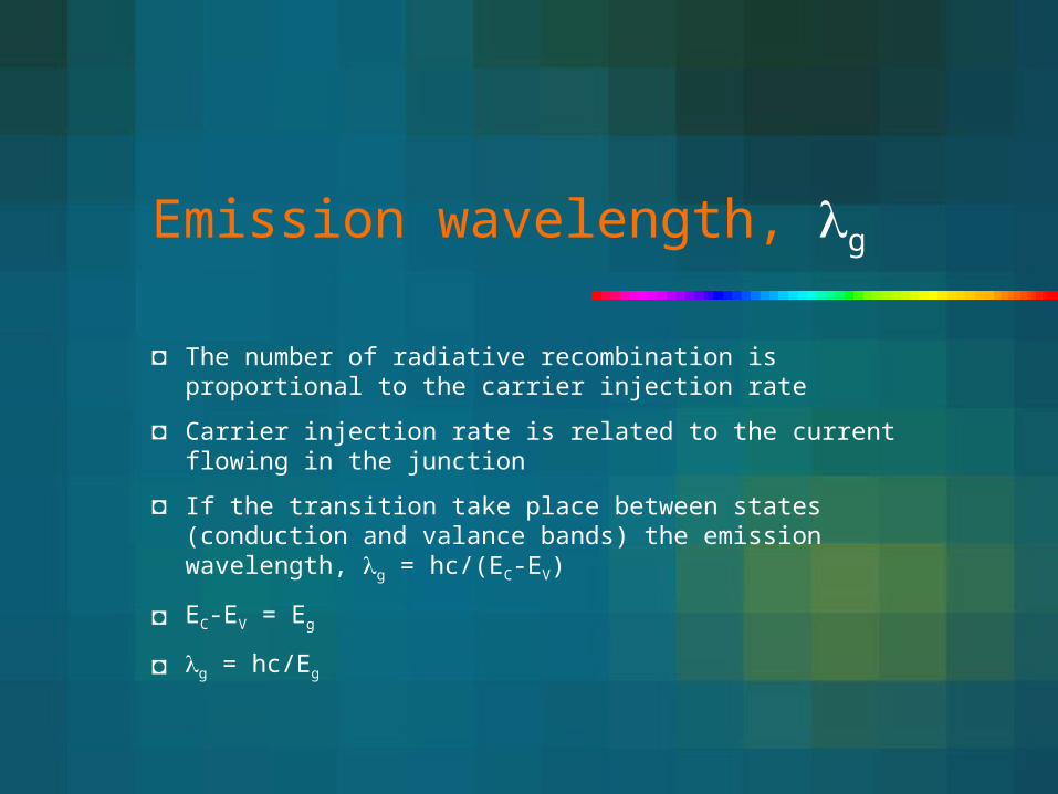
Emission wavelength, g
◘ The number of radiative recombination is proportional to the carrier injection rate
◘ Carrier injection rate is related to the current flowing in the junction
◘ If the transition take place between states (conduction and valance bands) the emission wavelength, g = hc/(EC-EV)
◘ EC-EV = Eg
◘ g = hc/Eg
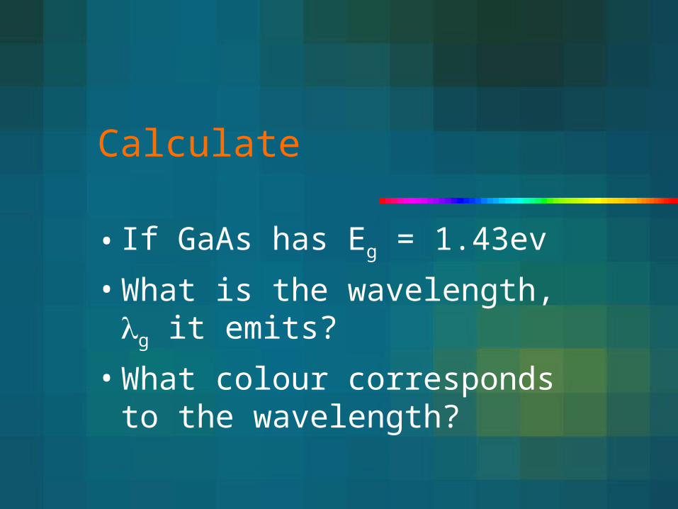
Calculate
• If GaAs has Eg = 1.43ev
• What is the wavelength, g it emits?• What colour corresponds to the
wavelength?
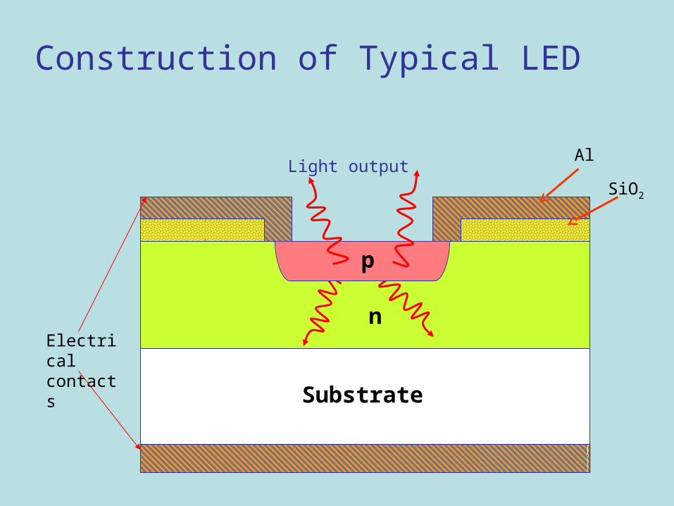
Construction of Typical LED
Substrate
n
Al
SiO2
Electrical contacts
p
Light output

LED Construction
Efficient light emitter is also an efficient absorbers of radiation therefore, a shallow p-n junction required.
Active materials (n and p) will be grown on a lattice matched substrate.
The p-n junction will be forward biased with contacts made by metallisation to the upper and lower surfaces.
Ought to leave the upper part ‘clear’ so photon can escape.
The silica provides passivation/device isolation and carrier confinement
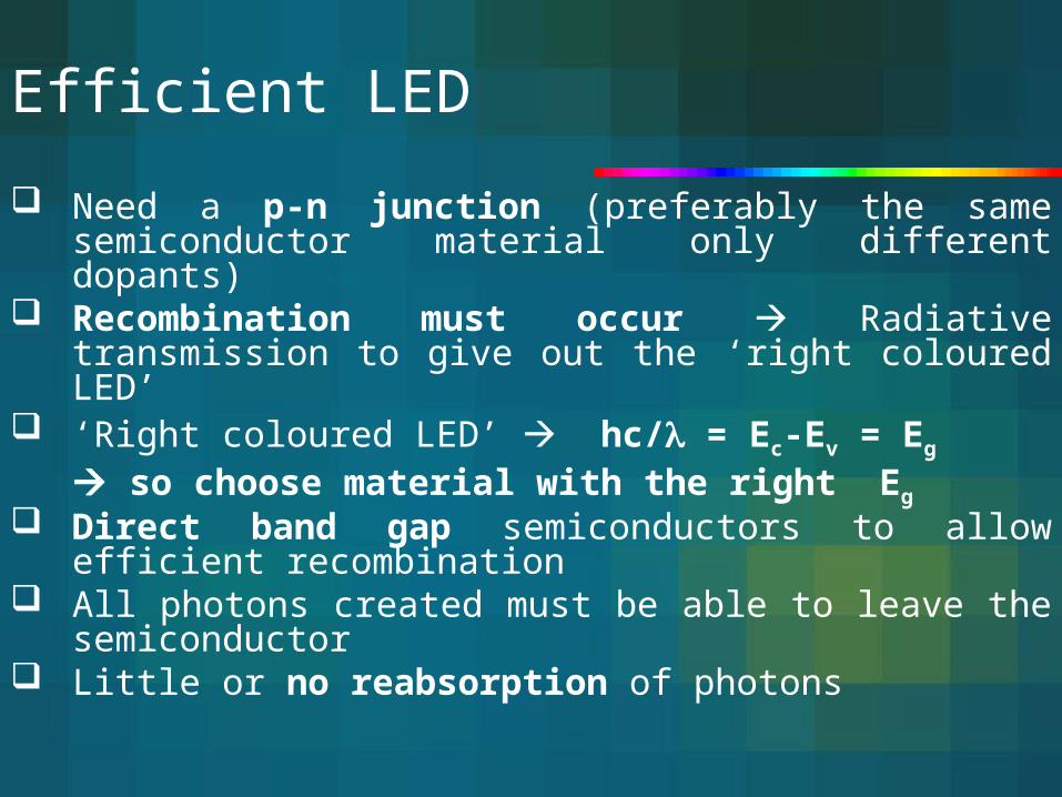
Efficient LED
Need a p-n junction (preferably the same semiconductor material only different dopants)
Recombination must occur Radiative transmission to give out the ‘right coloured LED’
‘Right coloured LED’ hc/ = Ec-Ev = Eg
so choose material with the right Eg
Direct band gap semiconductors to allow efficient recombination
All photons created must be able to leave the semiconductor
Little or no reabsorption of photons

Materials Requirements
Correct band gap Direct band gap
Material can be made p and n-type
Efficient radiative pathways must exist
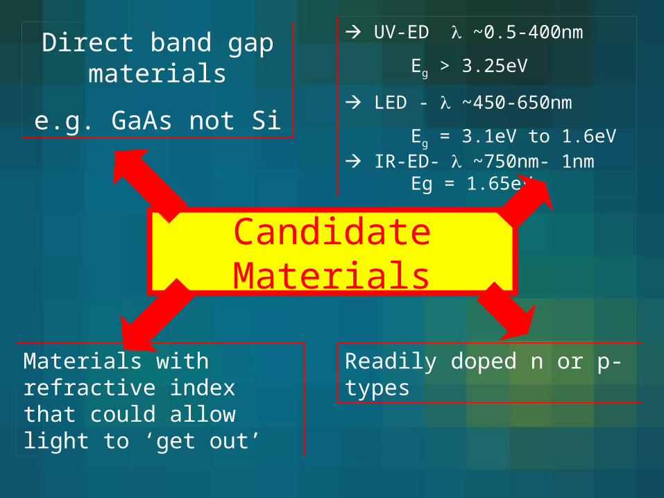
Candidate Materials
Direct band gap materials
e.g. GaAs not Si
UV-ED ~0.5-400nm
Eg > 3.25eV
LED - ~450-650nm
Eg = 3.1eV to 1.6eV IR-ED- ~750nm- 1nm
Eg = 1.65eV
Readily doped n or p-types
Materials with refractive index that could allow light to ‘get out’
Typical Exam Question
Describe the principles of operation of an LED and state the material’s requirements criteria to produce an efficient LED.
(50 marks)
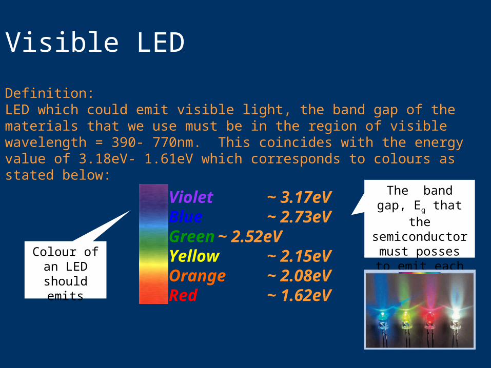
Visible LED
Definition:LED which could emit visible light, the band gap of the materials that we use must be in the region of visible wavelength = 390- 770nm. This coincides with the energy value of 3.18eV- 1.61eV which corresponds to colours as stated below:
Violet ~ 3.17eVBlue ~ 2.73eVGreen ~ 2.52eV Yellow ~ 2.15eVOrange ~ 2.08eVRed ~ 1.62eV
Colour of an LED should emits
The band gap, Eg that the
semiconductor must posses to emit each light
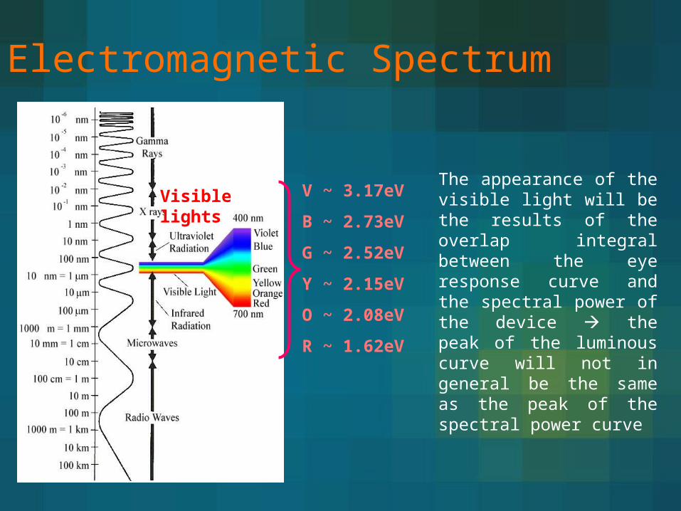
Electromagnetic Spectrum
Visible lights V ~ 3.17eV
B ~ 2.73eV
G ~ 2.52eV
Y ~ 2.15eV
O ~ 2.08eV
R ~ 1.62eV
The appearance of the visible light will be the results of the overlap integral between the eye response curve and the spectral power of the device the peak of the luminous curve will not in general be the same as the peak of the spectral power curve

Candidate Materials for LED’s
Question 1
• Indicate the binary compounds that can be selected for red, yellow, green and blue LED.
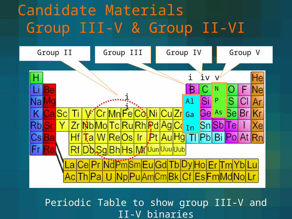
Candidate Materials Group III-V & Group II-VI
iviii v
ii
Periodic Table to show group III-V and II-V binaries
Group II Group III Group IV Group V
Al
Ga
In
N
P
As

Group III-V (1950)
The era of III–V compound semiconductors started in the early 1950s when this class of materials was postulated and demonstrated by Welker (1952, 1953). The class of III–V compounds had been an unknown substance prior to the 1950s that does not occur naturally. The novel man-made III–V compounds proved to be optically very active and thus instrumental to modern LED technology.

Group III-V LED materials
Al
Ga
In
N
P
As
AlN, AlP,AlAs
GaN, GaP, GaAs
InN, InP, InAs
GaAs GaP
GaAl
GaAsP
GaAsAl
Questions to ask when choosing the right material:1. Can it be doped or not?
2. What wavelength it can emit?3. Would the material able to allow radiative recombiation?
4. Direct or indirect semiconductor?
Questions to ask when choosing the right material:1. Can it be doped or not?
2. What wavelength it can emit?3. Would the material able to allow radiative recombiation?
4. Direct or indirect semiconductor?
Ternarycompounds
Binary compounds

Announcement
Evening classes


