44
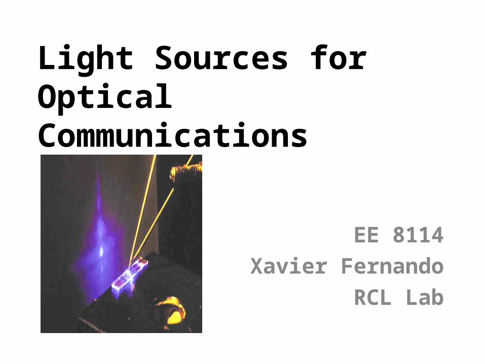
Light Sources for Optical Communications EE 8114 Xavier Fernando RCL Lab
| Date post: | 24-Dec-2015 |
| Category: |
Documents |
| Upload: | ruby-elliott |
| View: | 224 times |
| Download: | 4 times |
Light Sources for Optical Communications
EE 8114Xavier Fernando
RCL Lab

Requirements
• Small physical dimensions to suit the fiber• Narrow beam width to suit fiber NA • Narrow spectral width (or line width) to
reduce chromatic dispersion• Fast response time (high bandwidth) to
support high bit rate• High output power into the fiber for long
reach without repeaters

Considerations …• Ability to directly modulate by varying driving
current• Linearity (output light power proportional to
driving current) important for analog systems
• Stability LED better than LASER• Driving circuit issues impedance matching• Reliability (life time) and cost

Solid State (Semiconductor) Light Sources
• Light Emitting Diode (LED) Simple forward biased PN junction
• LASER Enhanced LED to achieve stimulated emission that provides:– Narrow line and beam widths, high output power
and coherent light
eV)(
24.1
m
hchEg

Energy-Bands
• Pure Group. IV (intrinsic semiconductor) material has equal number of holes and electrons.
• Thermal excitation of an electron from the valence band to the conduction band enable it to freely move.
-123 JK 1038.1 Bk

n-type material
• Donor level in an n-type (Group V) semiconductor. • The ionization of donor impurities creates an increased
electron concentration distribution.

p-type material
• Acceptor level in an p-type (Group III) semiconductor.
• The ionization of acceptor impurities creates an increased hole concentration distribution

Intrinsic & Extrinsic Materials
• Extrinsic material: donor or acceptor type semiconductors.
• Majority carriers: electrons in n-type or holes in p-type.• Minority carriers: holes in n-type or electrons in p-type.• The operation of semiconductor devices is essentially based on the
injection and extraction of minority carriers.
2inpn
)2
exp(Tk
Enpn
B
gi
ly.respective ionsconcentrat intrinsic & hole electron, theare && inpn
e.Temperatur is energy, gap theis TEg
Intrinsic material: A pure material with no impurities.
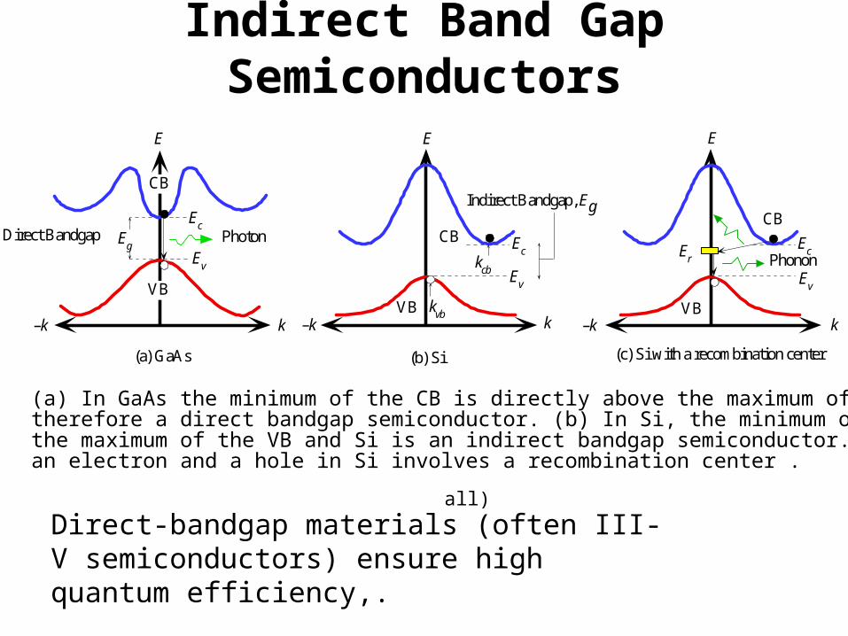
Indirect Band Gap Semiconductors
E
CB
k–k
Direct Bandgap
(a) GaAs
E
CB
VB
Indirect Bandgap, Eg
k–k
kcb
(b) Si
E
k–k
Phonon
(c) Si with a recombination center
Eg
Ec
Ev
Ec
Ev
kvb VB
CB
ErEc
Ev
Photon
VB
(a) In GaAs the minimum of the CB is directly above the maximum of the VB. GaAs istherefore a direct bandgap semiconductor. (b) In Si, the minimum of the CB is displaced fromthe maximum of the VB and Si is an indirect bandgap semiconductor. (c) Recombination ofan electron and a hole in Si involves a recombination center .
© 1999 S.O. Kasap, Optoelectronics (Prentice Hall)
Direct-bandgap materials (often III-V semiconductors) ensure high quantum efficiency,.
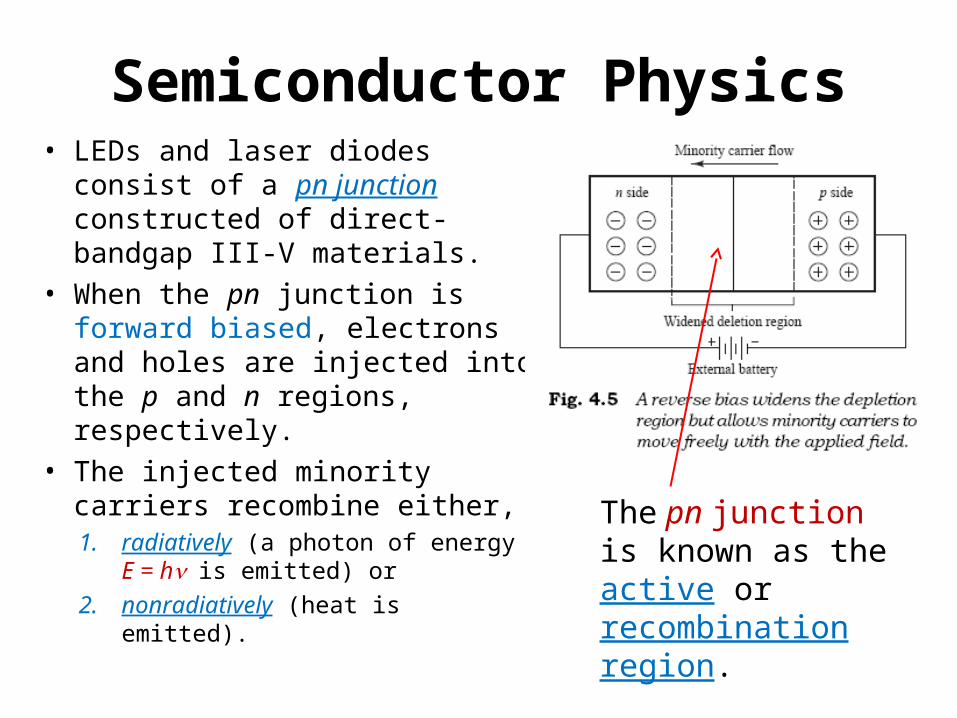
Semiconductor Physics• LEDs and laser diodes consist of a
pn junction constructed of direct-bandgap III-V materials.
• When the pn junction is forward biased, electrons and holes are injected into the p and n regions, respectively.
• The injected minority carriers recombine either,1. radiatively (a photon of energy E = h
is emitted) or 2. nonradiatively (heat is emitted).
The pn junction is known as the active or recombination region.

Wavelength Bands and Materials
Band Description Wavelength range
O band original 1260–1360 nm
E band extended 1360–1460 nm
S band short wavelengths
1460–1530 nm
C band conventional (“erbium window”)
1530–1565 nm
L band long wavelengths
1565–1625 nm
U band ultralong wavelengths
1625–1675 nm

Physical Design of an LED• An LED emits incoherent, non-directional, and
unpolarized spontaneous photons. • An LED does not have a threshold current.• Double hetero structure (2 p type and 2 n type
materials) is used to improve light output• Each region shall also have the right refractive
index to guide the light (optical property)• Light exits via the surface (SLED) or the edge
(ELED)
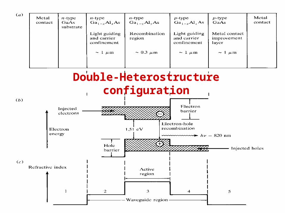
Double-Heterostructure configuration

Light-Emitting DiodesLED features:• Made of GaAlAs (850 nm) or InGaAsP (S-L bands)• Broad spectral output (50 to 150 nm)• Optical output powers less than -13 dBm (50 μW)• Can be modulated only up a few hundred Mb/s• Less expensive than laser diodes• Edge-emitter or surface emitter structures
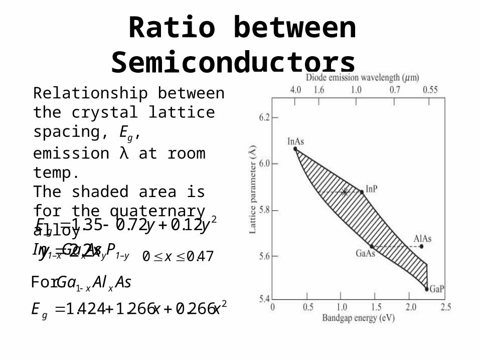
Ratio between Semiconductors
2
1
266.0266.1424.1
For
xxE
AsAlGa
g
xx
Relationship between the crystal lattice spacing, Eg, emission λ at room temp. The shaded area is for the quaternary alloy In1–xGaxAsyP1–y
xy 2.2 47.00 x
212.072.035.1 yyEg

Bandgap EnergyThe source emission wavelength depends on the bandgap
energy of the device material.
16

Bandgap Energy For In1–xGaxAsyP1–y compositions that are lattice-
matched to InP, the bandgap in eV varies as
17
Bandgap wavelengths from 920 to 1650 nm are covered by this material system.
xy 2.2 47.00 x
212.072.035.1 yyEg
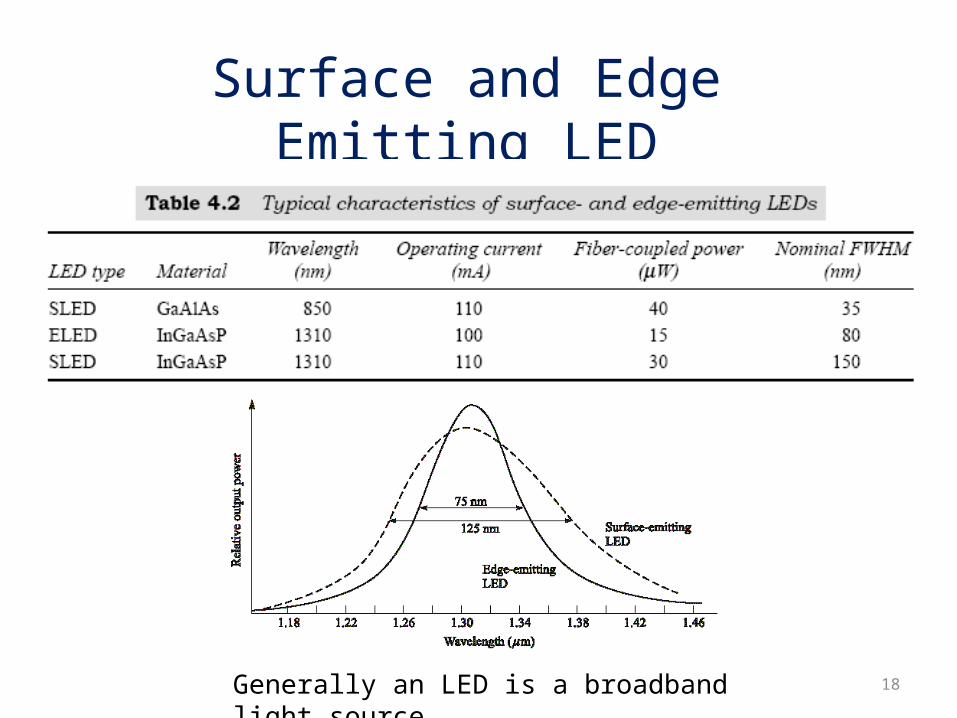
Surface and Edge Emitting LED
18Generally an LED is a broadband light source
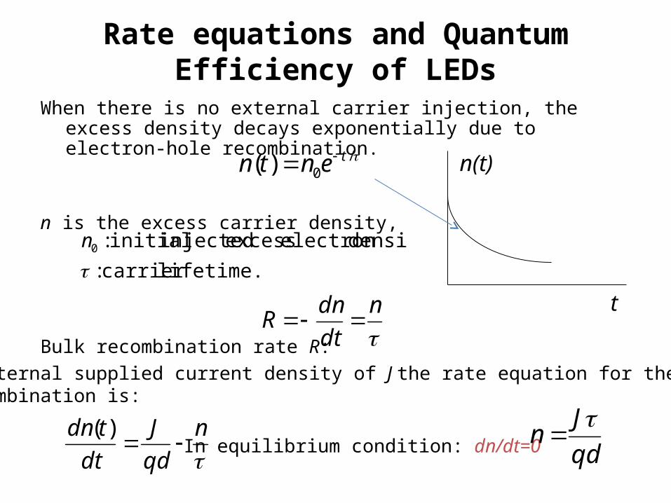
Rate equations and Quantum Efficiency of LEDs
When there is no external carrier injection, the excess density decays exponentially due to electron-hole recombination.
n is the excess carrier density,
Bulk recombination rate R:
/0)( tentn
lifetime.carrier :
densityelectron excess injected initial :0
n
n
dt
dnR
t
n(t)
With an external supplied current density of J the rate equation for the electron-hole recombination is:
n
qd
J
dt
tdn
)(In equilibrium condition: dn/dt=0 qd
Jn

nrnrr /τ/τ/τRRR 1 11 r
t
n(t)
Bulk recombination rate (R) = Radiative recombination rate (Rr) + Nonradiative recombination rate (Rnr)
For exponential decay of excess carriers: Radiative recombination lifetime τr=n/Rr Nonradiative recombination lifetime τnr=n/Rnr
rte /
nrte /
/te
For high quantum efficiency, Rr >> Rnr τr << τnr

Quantum Efficiency
Internal quantum efficiency is the ratio between the radiative recombination rate and the sum of radiative and nonradiative recombination rates
qIRRR
RR
R
nrrr
rnrr
nr
nrr
r
/)(int
int
Where, the current injected into the LED is I, and q is the charge of an electron.
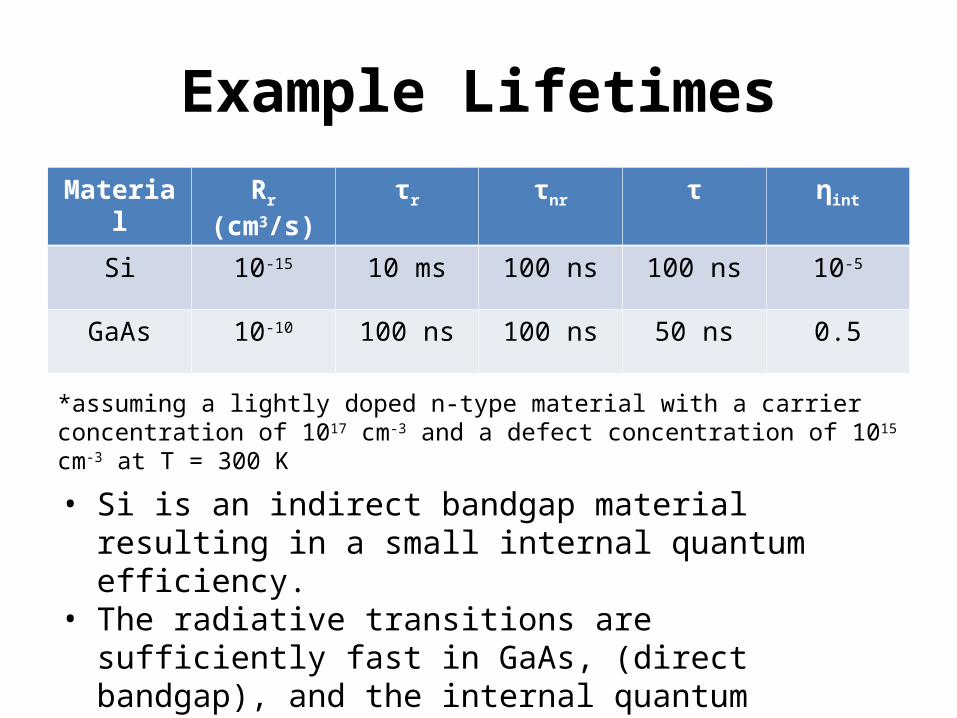
Example LifetimesMaterial Rr (cm3/s) τr τnr τ ηint
Si 10-15 10 ms 100 ns 100 ns 10-5
GaAs 10-10 100 ns 100 ns 50 ns 0.5
*assuming a lightly doped n-type material with a carrier concentration of 1017 cm-3 and a defect concentration of 1015 cm-3 at T = 300 K
• Si is an indirect bandgap material resulting in a small internal quantum efficiency.
• The radiative transitions are sufficiently fast in GaAs, (direct bandgap), and the internal quantum efficiency is large.

Internal Quantum Efficiency & Optical Power
Optical power generated internally in the active region in the LED is equal to the number of photons/seconds (I/q) timesenergy per photons (hv) times the internal quantum efficiency
I
q
hcIh
q
IP intintintint 24.1
[4-9]
region active current to Injected :
power, optical Internal :int
I
P

External Efficiency• Only a small portion of internally generated
the light exits the LED due to:– Absorption losses α exp(-αl), where α is the
absorption coefficient and l is the path length– Fresnel reflection losses, that increases with the
angle of incidence– Loss due to total internal reflection (TIR) which
results in a small ‘escape cone’
photons generated internally of #
LED from emitted photons of #ext

Fresnel Reflection• Whenever light travels from a medium of refractive index n1
to a medium of index n2, then Fresnel reflection will happen.
• For perpendicular incidence the F. R. is given by,
• R is the Fresnel reflectivity at the fiber-core end face; • T is the Fresnel transmissivity (Note R+T = 1)
Note: When the amplitudes of the light is considered, the reflection coefficient r = (n1 – n2)/(n1 + n2) relates the incident and reflected wave.
221
21
)(
4
nn
nnT
2
21
21
nn
nnR

Fresnel Reflection Example
26
In general At the surface of any two material with n1 and n2 ref indices, there will be Fresnel Loss
Fresnel Loss = -10 Log (T)

dTc
)sin2()(4
1
0
ext
221
21
)(
4)0(tCoefficienon Transmissi Fresnel :)(
nn
nnTT
[4-12]
211
ext2 )1(
11 If
nnn [4-13]
211
intintext )1(
powr, optical emitted LED
nn
PPP [4-14]
LED Light emission cone
n1
n2

The fraction of light lies within the escape cone from a point source:
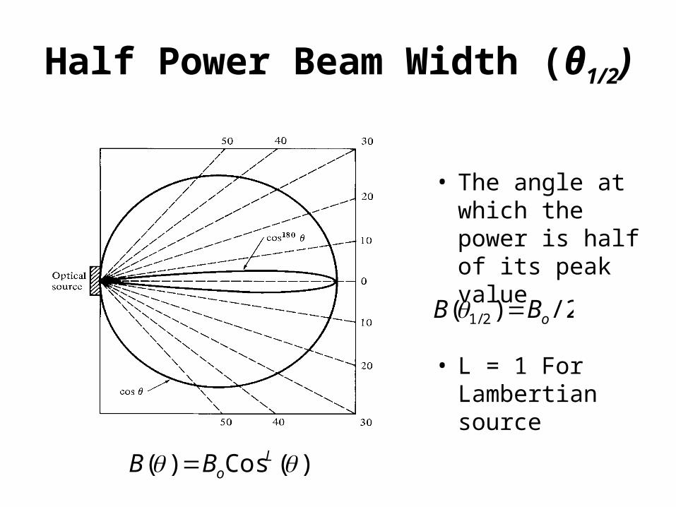
Half Power Beam Width (θ1/2)
• The angle at which the power is half of its peak value
• L = 1 For Lambertian source
)(Cos)( LoBB
/2)( 2/1 oBB
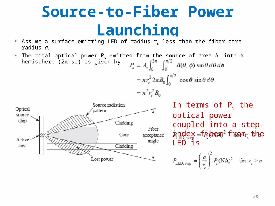
Source-to-Fiber Power Launching• Assume a surface-emitting LED of radius rs less than the fiber-core radius a.• The total optical power Ps emitted from the source of area As into a hemisphere
(2π sr) is given by
30
In terms of Ps the optical power coupled into a step-index fiber from the LED is

Modulation of an LED• The response time of an optical source determines how fast
an electrical input drive signal can vary the light output level• If the drive current is modulated at a frequency ω and P0 is the
power emitted at zero modulation frequency, the optical output power of the device will vary as

3-dB bandwidths
Optical Power I(f); Electrical Power I2(f)
2)2(1/)( fPfP o
Electrical Loss = 2 x Optical Loss

Modulation of LED• The frequency response of an LED depends on:
1- Doping level in the active region
2- Injected carrier lifetime in the recombination region, .
3- Parasitic capacitance of the LED
• If the drive current of an LED is modulated at a frequency of ω, the output optical power of the device will vary as:
• Electrical current is directly proportional to the optical power, thus we can define electrical bandwidth and optical bandwidth, separately.
[4-15]
i
current electrical : power, electrical:
)0(log20
)0(10log BW Electrical
Ip
I
)I(
p
)p(
[4-16]
)0(
)(log10
)0(
)(log10 BW Optical
I
I
P
P

Electrical and Optical Bandwidths
t0
Pi = Input light power
Emitter
OpticalInput
OpticalOutput
Fiber
PhotodetectorSinusoidal signal
Sinusoidal electrical signalt
t0
f1 kHz 1 MHz 1 GHz
Po / Pi
fop
0.1
0.05
f = Modulation frequency
An optical fiber link for transmitting analog signals and the effect of dispersion in thefiber on the bandwidth, fop.
Po = Output light power
Electrical signal (photocurrent)
fel
10.707
f1 kHz 1 MHz 1 GHz
© 1999 S.O. Kasap, Optoelectronics (Prentice Hall)
Drawbacks of LED
• Large line width (30-40 nm)• Large beam width (Low coupling to the fiber)• Low output power • Low E/O conversion efficiencyAdvantages• Robust • Linear

Source-to-Fiber Power CouplingComparison of the optical powers coupled into two step-index fibers
36
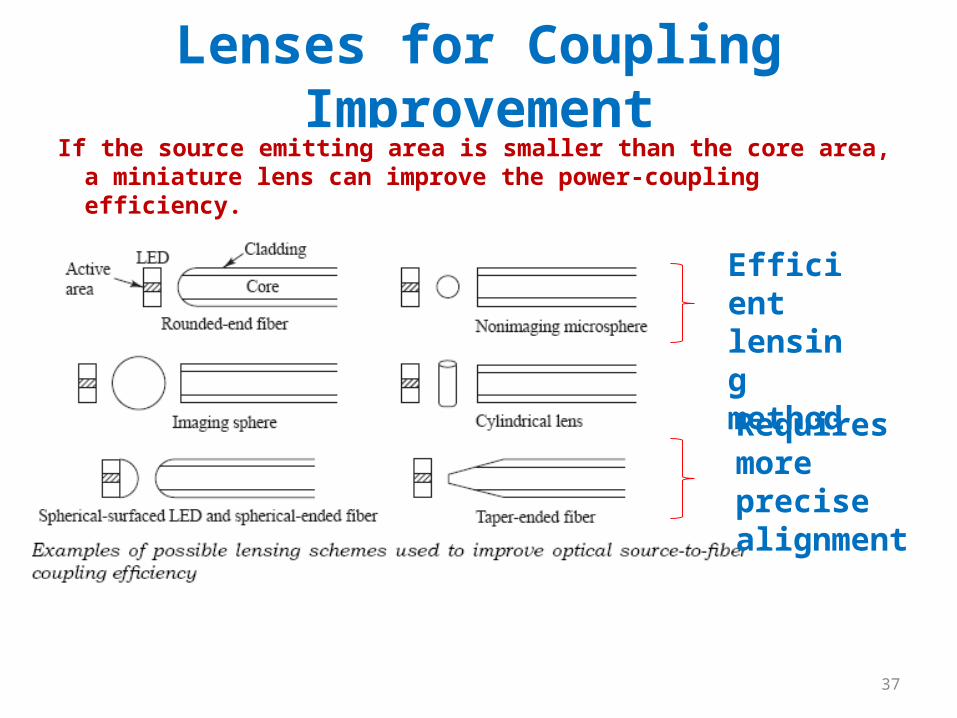
Lenses for Coupling ImprovementIf the source emitting area is smaller than the core area, a
miniature lens can improve the power-coupling efficiency.
37
Efficient lensing method
Requires more precise alignment

Fiber-to-Fiber Joints• Different modal distributions of the optical beam emerging
from a fiber result in different degrees of coupling loss.
38
A steady-state modal equilibrium has been established in the emitting fiber.
All modes in the emitting fiber are equally excited. Achieving a steady-state in the receiving fiber results in an additional loss.

Mechanical Misalignment
• For a receiving fiber to accept all the optical power emitted by the first fiber, there must be perfect mechanical alignment between the two fibers, and their geometric and waveguide characteristics must match precisely.
• Mechanical alignment is a major problem in joining fibers.
39
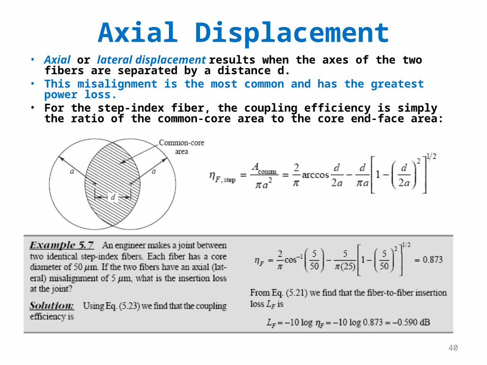
Axial Displacement• Axial or lateral displacement results when the axes of the two fibers are
separated by a distance d.• This misalignment is the most common and has the greatest power loss.• For the step-index fiber, the coupling efficiency is simply the ratio of the
common-core area to the core end-face area:
40
Optical Fiber Connectors
Principal requirements of a good connectors:1. Low coupling losses. The connector assembly must maintain stringent alignment
tolerances to assure low mating losses. These low losses must not change significantly during operation or after numerous connects and disconnects.
2. Interchangeability. Connectors of the same type must be compatible from one manufacturer to another.
3. Ease of assembly. A technician should be able to install the connector easily in a field environment. The connector loss should also be fairly insensitive to the assembly skill of the technician.
4. Low environmental sensitivity. Conditions such as temperature, dust, and moisture should have a small effect on connector-loss variations.
5. Low cost and reliable construction. The connector must have a precision suitable to the application, but its cost must not be a major factor in the fiber system.
6. Ease of connection. One should be able to mate the connector by hand
41
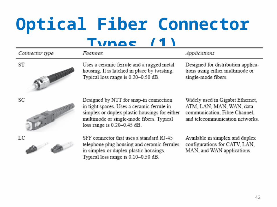
Optical Fiber Connector Types (1)
42
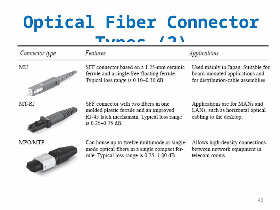
Optical Fiber Connector Types (2)
43

Angular Misalignment• When two fiber ends are separated longitudinally by a gap s,
not all the higher-mode optical power emitted in the ring of width x will be intercepted by the receiving fiber.
• The loss for an offset joint between two identical step-index fibers is
44


