Page 1
1/12 www.rohm.com Dec.2015 - Rev. A© 2015 ROHM Co., Ltd. All rights reserved.
Linear Regulator Series
Linear Regulator Specifications
A linear regulator data sheet includes a specifications table
that lists output voltage values and precision. Besides, very
important information such as maximum ratings, operating
conditions and characteristic graphs are described in the
table.
The absolute maximum rating is defined as a value that must
not be exceeded even for a moment. Although some items
are defined by a time component, such as short-circuit time, it
is basically prohibited to exceed the absolute maximum rating
in every case. And, for obvious reasons, a tolerance like
±10% is never assigned to values. We sometimes receive
questions like: What will happen if a value exceeds the
absolute maximum rating? How much margin does the
system have? (These questions may be just a matter of
interest.) However, they miss the point when it comes to
considering the purpose of absolute maximum rating. You
should make efforts so that the operating maximum value will
not exceed the maximum rating or try to use a linear regulator
model having the maximum rating that allows the operating
maximum value.
It is important to identify the conditions that guarantee the
specification values, for example, applied voltage and
temperature. Actual use conditions do not always accord
with specification-stipulated conditions. As a typical
example, if a condition of Ta=25°C is given, its guaranteed
value persistently is a value at Ta=25°C. However, in actual
use, a constant condition at Ta=25°C would be possible only
in a thermostatic bath. Therefore, in examining the
specification value, it is necessary to verify whether the value
applies to a single specific condition or a range of conditions,
for example, a range of operating temperatures, and to
confirm the value in a condition close to the actual use
condition and operating condition of the designed equipment.
To do this, a supplemental reference graph is often useful.
Lastly, the specification values include descriptions of any
one or all of the minimum values (Min), maximum values
(Max) and typical values (Typ). Among these, only the
minimum value and maximum value are guaranteed. The
typical value (Typ) is “an approximate value” based on
characteristic distributions and statistical techniques.
Basically, every product is designed based on the
specification values. Then, which value should we use to
design products? Although general designs might be based
on typical values in principle, the design should be based on
the values that pose the worst conditions. This selection
depends on the know-how and experience of designers
themselves.
This paper explains typical items in linear regulator
specifications. However, other specification items may not
be ignored. Reading a data sheet carefully is very important
for designers, not only for linear regulators but also for other
equipment.
No.15020EAY18
Page 2
Application Note
2/12 www.rohm.com Dec.2015 - Rev. A© 2015 ROHM Co., Ltd. All rights reserved.
Linear Regulator Specifications
Table of Contents
1. Input Power Supply Voltage Range ................................................................... 3 2. Output Voltage Range ........................................................................................ 3 3. Output Voltage Precision .................................................................................... 4 4. Output Current ................................................................................................... 4 5. Input/Output Voltage Difference ......................................................................... 4 6. Transient Response Characteristics ................................................................... 5 7. Ripple Rejection Ratio ........................................................................................ 6 8. Circuit Current .................................................................................................... 7 9. EN Pin (CTL/STBY Pin) ..................................................................................... 8 10. Line regulation ................................................................................................. 9 11. Load Regulation ............................................................................................... 9 12. Output Discharge ............................................................................................. 9 13. Soft Start ........................................................................................................ 10 14. Input Capacitor ............................................................................................... 10 15. Output Capacitor ............................................................................................ 10 16. Power Dissipation .......................................................................................... 11 17. Overcurrent Protection ................................................................................... 11 18. Thermal Shut Down ....................................................................................... 12
Page 3
Application Note
3/12 www.rohm.com Dec.2015 - Rev. A© 2015 ROHM Co., Ltd. All rights reserved.
Linear Regulator Specifications
1. Input Power Supply Voltage Range
The input power supply voltage range identifies two values.
The range indicated in the absolute maximum rating shows
the applicable extent of “input,” or the limitation of voltage
application. This does not mean that the linear regulator
operates normally within the given range. We check that the
value is within this range, assuming an irregular voltage
value.
Apart from the absolute maximum rating, the items entitled
"recommended input range" and "operating input range" are
given. Thus, you may refer to these items.
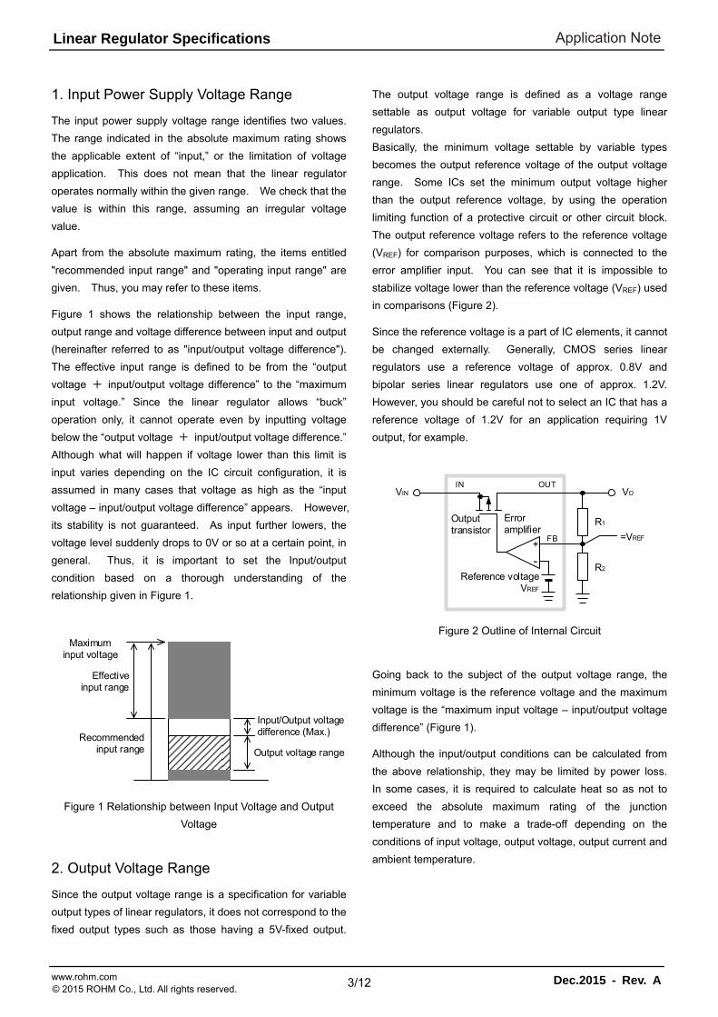
Figure 1 shows the relationship between the input range,
output range and voltage difference between input and output
(hereinafter referred to as "input/output voltage difference").
The effective input range is defined to be from the “output
voltage + input/output voltage difference” to the “maximum
input voltage.” Since the linear regulator allows “buck”
operation only, it cannot operate even by inputting voltage
below the “output voltage + input/output voltage difference.”
Although what will happen if voltage lower than this limit is
input varies depending on the IC circuit configuration, it is
assumed in many cases that voltage as high as the “input
voltage – input/output voltage difference” appears. However,
its stability is not guaranteed. As input further lowers, the
voltage level suddenly drops to 0V or so at a certain point, in
general. Thus, it is important to set the Input/output
condition based on a thorough understanding of the
relationship given in Figure 1.
Input/Output voltage difference (Max.)
Recommended input range Output voltage range
Effectiveinput range
Maximum input voltage
Figure 1 Relationship between Input Voltage and Output
Voltage
2. Output Voltage Range
Since the output voltage range is a specification for variable
output types of linear regulators, it does not correspond to the
fixed output types such as those having a 5V-fixed output.
The output voltage range is defined as a voltage range
settable as output voltage for variable output type linear
regulators.
Basically, the minimum voltage settable by variable types
becomes the output reference voltage of the output voltage
range. Some ICs set the minimum output voltage higher
than the output reference voltage, by using the operation
limiting function of a protective circuit or other circuit block.
The output reference voltage refers to the reference voltage
(VREF) for comparison purposes, which is connected to the
error amplifier input. You can see that it is impossible to
stabilize voltage lower than the reference voltage (VREF) used
in comparisons (Figure 2).
Since the reference voltage is a part of IC elements, it cannot
be changed externally. Generally, CMOS series linear
regulators use a reference voltage of approx. 0.8V and
bipolar series linear regulators use one of approx. 1.2V.
However, you should be careful not to select an IC that has a
reference voltage of 1.2V for an application requiring 1V
output, for example.
IN OUT
FB+
VIN VO
-
VREF
Reference voltage
Error amplifier
R1
R2
=VREF
Output transistor
Figure 2 Outline of Internal Circuit
Going back to the subject of the output voltage range, the
minimum voltage is the reference voltage and the maximum
voltage is the “maximum input voltage – input/output voltage
difference” (Figure 1).
Although the input/output conditions can be calculated from
the above relationship, they may be limited by power loss.
In some cases, it is required to calculate heat so as not to
exceed the absolute maximum rating of the junction
temperature and to make a trade-off depending on the
conditions of input voltage, output voltage, output current and
ambient temperature.
Page 4
Application Note
4/12 www.rohm.com Dec.2015 - Rev. A© 2015 ROHM Co., Ltd. All rights reserved.
Linear Regulator Specifications
3. Output Voltage Precision
Output voltage precision is the output voltage tolerance of the
fixed output types of linear regulators. While ±5% used to be
the standard tolerance, high precision types of ±1% are
widely available as of recent. Output voltage precision has a
close relationship with temperature and output current.
Output voltage precision for variable output types of linear
regulators corresponds to the precision of the reference
voltage VREF. This becomes the precision of the IC itself.
Output voltage of variable output types is set by external
resistors. Therefore, output precision of variable output
types is calculated by adding the “tolerance of the resistors
set as the output” to the “precision of the reference voltage”.
The value of the resistors set as output conforms to the
setting range in the data sheet, if any. For the bipolar type
linear regulators, the error amplifier income current exists in
the feedback pin. If the resistance value is too large, the
current causes a voltage drop, which will cause an error in
output voltage. On the contrary, if the resistance value is too
small, the voltage error is reduced but the current capacity is
also reduced, which will disable the normal feedback trigger
for IC startup.
4. Output Current
The output current specifications stipulate the allowable
output current range. Some data sheets stipulate the
maximum value only. The maximum value means that
output is allowed up to this value. Actually, current over this
value flows. You must be careful with the maximum value
because it has happened that the load was damaged due to a
misunderstanding of the current limit to be applied at the
indicated value. To check the limit value, you should refer to
the overcurrent protection detection current or a characteristic
graph by item. When this current is known, it will help
determine measures for worst case conditions.
Then, is it possible to use the guaranteed output current all
the time? Output current is limited by the junction
temperature absolute maximum rating, keeping in mind the
input/output conditions and ambient temperature conditions.
For a linear regulator, heat calculation is one of the important
items that is always required.
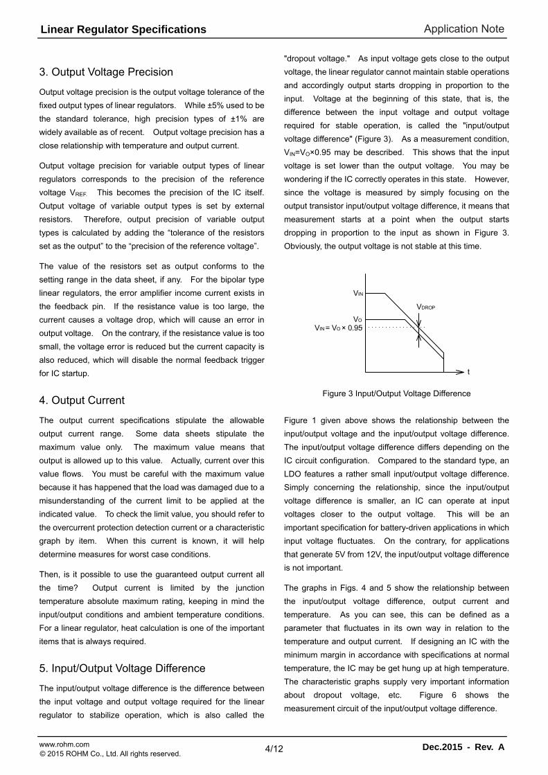
5. Input/Output Voltage Difference
The input/output voltage difference is the difference between
the input voltage and output voltage required for the linear
regulator to stabilize operation, which is also called the
"dropout voltage." As input voltage gets close to the output
voltage, the linear regulator cannot maintain stable operations
and accordingly output starts dropping in proportion to the
input. Voltage at the beginning of this state, that is, the
difference between the input voltage and output voltage
required for stable operation, is called the "input/output
voltage difference" (Figure 3). As a measurement condition,
VIN=VO×0.95 may be described. This shows that the input
voltage is set lower than the output voltage. You may be
wondering if the IC correctly operates in this state. However,
since the voltage is measured by simply focusing on the
output transistor input/output voltage difference, it means that
measurement starts at a point when the output starts
dropping in proportion to the input as shown in Figure 3.
Obviously, the output voltage is not stable at this time.
VIN
VO
t
VDROP
VIN = VO × 0.95
Figure 3 Input/Output Voltage Difference
Figure 1 given above shows the relationship between the
input/output voltage and the input/output voltage difference.
The input/output voltage difference differs depending on the
IC circuit configuration. Compared to the standard type, an
LDO features a rather small input/output voltage difference.
Simply concerning the relationship, since the input/output
voltage difference is smaller, an IC can operate at input
voltages closer to the output voltage. This will be an
important specification for battery-driven applications in which
input voltage fluctuates. On the contrary, for applications
that generate 5V from 12V, the input/output voltage difference
is not important.
The graphs in Figs. 4 and 5 show the relationship between
the input/output voltage difference, output current and
temperature. As you can see, this can be defined as a
parameter that fluctuates in its own way in relation to the
temperature and output current. If designing an IC with the
minimum margin in accordance with specifications at normal
temperature, the IC may be get hung up at high temperature.
The characteristic graphs supply very important information
about dropout voltage, etc. Figure 6 shows the
measurement circuit of the input/output voltage difference.
Page 5
Application Note
5/12 www.rohm.com Dec.2015 - Rev. A© 2015 ROHM Co., Ltd. All rights reserved.
Linear Regulator Specifications
Figure 4 Input/Output Voltage Difference – Output Current
Figure 5 Input/Output Voltage Difference – Ambient
Temperature
IN OUT
FBGND
VIN
VO
IO
V
VDROP
CIN COR1
R2
Figure 6 Input/Output Voltage Difference Measurement
Circuit
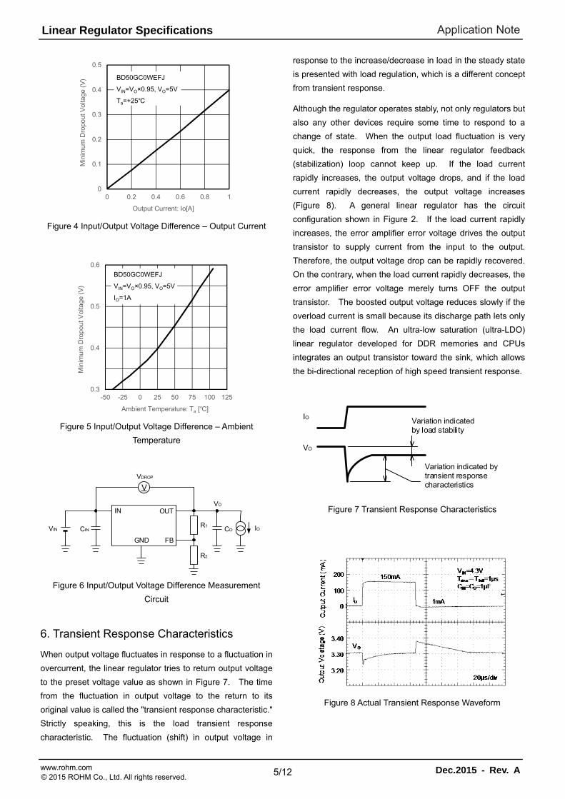
6. Transient Response Characteristics
When output voltage fluctuates in response to a fluctuation in
overcurrent, the linear regulator tries to return output voltage
to the preset voltage value as shown in Figure 7. The time
from the fluctuation in output voltage to the return to its
original value is called the "transient response characteristic."
Strictly speaking, this is the load transient response
characteristic. The fluctuation (shift) in output voltage in
response to the increase/decrease in load in the steady state
is presented with load regulation, which is a different concept
from transient response.
Although the regulator operates stably, not only regulators but
also any other devices require some time to respond to a
change of state. When the output load fluctuation is very
quick, the response from the linear regulator feedback
(stabilization) loop cannot keep up. If the load current
rapidly increases, the output voltage drops, and if the load
current rapidly decreases, the output voltage increases
(Figure 8). A general linear regulator has the circuit
configuration shown in Figure 2. If the load current rapidly
increases, the error amplifier error voltage drives the output
transistor to supply current from the input to the output.
Therefore, the output voltage drop can be rapidly recovered.
On the contrary, when the load current rapidly decreases, the
error amplifier error voltage merely turns OFF the output
transistor. The boosted output voltage reduces slowly if the
overload current is small because its discharge path lets only
the load current flow. An ultra-low saturation (ultra-LDO)
linear regulator developed for DDR memories and CPUs
integrates an output transistor toward the sink, which allows
the bi-directional reception of high speed transient response.
VO
IO
Variation indicated by transient response characteristics
Variation indicated by load stability
Figure 7 Transient Response Characteristics
Figure 8 Actual Transient Response Waveform
0
0.1
0.2
0.3
0.4
0.5
0 0.2 0.4 0.6 0.8 1
Min
imum
Dro
pout
Vol
tage
(V)
Output Current: Io[A]
BD50GC0WEFJVIN=VO×0.95, VO=5VTa=+25
0.3
0.4
0.5
0.6
-50 -25 0 25 50 75 100 125
Min
imum
Dro
pout
Vol
tage
(V)
Ambient Temperature: Ta []
BD50GC0WEFJVIN=VO×0.95, VO=5VIO=1A
Page 6
Application Note
6/12 www.rohm.com Dec.2015 - Rev. A© 2015 ROHM Co., Ltd. All rights reserved.
Linear Regulator Specifications
Figure 9 shows a transient response characteristics
measurement circuit. Two types of load resistors are
provided to change the current value quickly via a transistor.
When a load device is integrated, the load type is set to the
CR mode to change the load by time-sharing and measure
the response. The output current is monitored by a current
probe, and the output voltage is measured by a voltage
probe.
For applications subject to rapid changes in load current,
transient response characteristics are critical factors. If the
recovery of an output voltage that has been dramatically
changed by load fluctuation is delayed, failures may arise; for
example, the circuit may be reset or a data error may occur.
To minimize such failures, it is necessary to select a linear
regulator with excellent transient response characteristics.
Although a switching regulator also has transient response
characteristics, the characteristics of a linear regulator ensure
relatively high speed thanks to its continuous loop control.
However, transient response characteristics are not
guaranteed as a specification in most cases. This is
because transient response characteristics are influenced by
output capacity and wiring inductance, and, accordingly, it is
impossible to determine defaults as a rule. You may refer to
the characteristic values of a standard circuit example in a
graph, if available. But, in the end, we still recommend
measuring the transient response characteristics using real
equipment because they vary also depending on the PCB
layout as mentioned above.
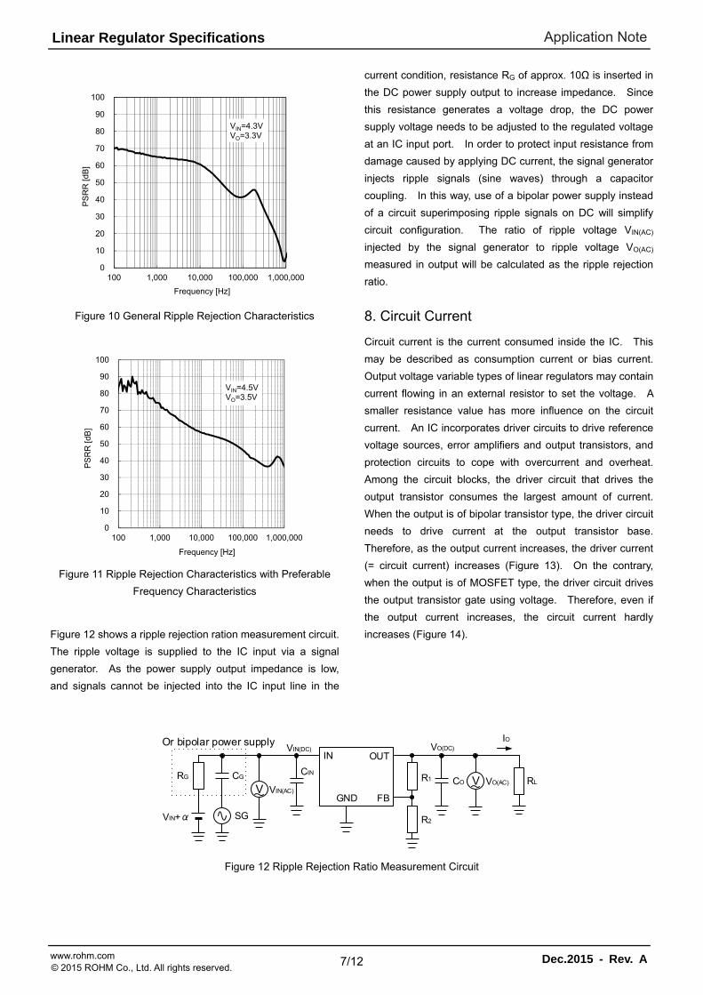
7. Ripple Rejection Ratio
Ripple rejection ratio is a specification that stipulates how
much ripple voltage in input can be removed in output. It is
also called PSRR, input voltage ripple rejection rate, as well
as other things, but regardless of what it is called, its
significance is the same. Ripple rejection ratio is often
presented in units of dB. For example, 60dB means that
input ripple is reduced to 1/1000, and ripple of 100mV may be
reduced to 0.1mV.
RippleRejectionRatio 20 logOutputRippleVoltageInputRippleVoltage
Ripple rejection ratio becomes important when the input
ripple is large. Recently, switching regulators have become
popular to the point that even applications where noise is a
problem are likely to use switching regulators from the
viewpoint of efficiency. However, some applications that
cannot compromise S/N ratio may use the ripple rejection
function of linear regulators in order to remove switching
noise (ripple) in the output from switching regulators.
Although this is indeed one of the effective solutions, it is
necessary to carefully examine the input ripple frequency and
frequency characteristics of the ripple rejection ratio.
Generally, ripple rejection performance deteriorates as the
frequency gets higher. Therefore, in cases having a high
ripple frequency, the expected efficiency may not be obtained.
Figure 10 shows ripple rejection characteristics of a common
linear regulator, in which the removal ratio against frequency
gets lower. For example, approx. 5dB is measured at 1MHz,
which means a removal ratio as small as 1/1.8. On the
contrary, the switching frequency of switching regulators is as
high as several hundreds kHz to several MHz. For example,
if a 1MHz switching regulator has ripple of 100mV, ripple of
56mV is left. Recently, linear regulators with improved
frequency characteristics have been developed. The
example in Figure 11 shows that the ripple rejection ratio is
35dB at 1MHz and that ripple can be reduced to 1/56, that is,
1.8mV.
Figure 9 Transient Response Characteristics Measurement Circuit
IN OUT
FBGND
VOIO
Current Probe
Or electronic loadCR modeCIN
COR1
R2
RL1 RL2
Page 7
Application Note
7/12 www.rohm.com Dec.2015 - Rev. A© 2015 ROHM Co., Ltd. All rights reserved.
Linear Regulator Specifications
Figure 10 General Ripple Rejection Characteristics
Figure 11 Ripple Rejection Characteristics with Preferable
Frequency Characteristics
Figure 12 shows a ripple rejection ration measurement circuit.
The ripple voltage is supplied to the IC input via a signal
generator. As the power supply output impedance is low,
and signals cannot be injected into the IC input line in the
current condition, resistance RG of approx. 10Ω is inserted in
the DC power supply output to increase impedance. Since
this resistance generates a voltage drop, the DC power
supply voltage needs to be adjusted to the regulated voltage
at an IC input port. In order to protect input resistance from
damage caused by applying DC current, the signal generator
injects ripple signals (sine waves) through a capacitor
coupling. In this way, use of a bipolar power supply instead
of a circuit superimposing ripple signals on DC will simplify
circuit configuration. The ratio of ripple voltage VIN(AC)
injected by the signal generator to ripple voltage VO(AC)
measured in output will be calculated as the ripple rejection
ratio.
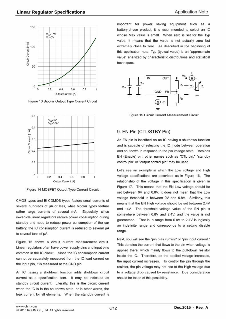
8. Circuit Current
Circuit current is the current consumed inside the IC. This
may be described as consumption current or bias current.
Output voltage variable types of linear regulators may contain
current flowing in an external resistor to set the voltage. A
smaller resistance value has more influence on the circuit
current. An IC incorporates driver circuits to drive reference
voltage sources, error amplifiers and output transistors, and
protection circuits to cope with overcurrent and overheat.
Among the circuit blocks, the driver circuit that drives the
output transistor consumes the largest amount of current.
When the output is of bipolar transistor type, the driver circuit
needs to drive current at the output transistor base.
Therefore, as the output current increases, the driver current
(= circuit current) increases (Figure 13). On the contrary,
when the output is of MOSFET type, the driver circuit drives
the output transistor gate using voltage. Therefore, even if
the output current increases, the circuit current hardly
increases (Figure 14).
IN OUT
FBGND
VIN+α
VO(DC)
IO
CIN
COR1
R2
RLRG
SG
CG
VIN(DC)
V VIN(AC)V VO(AC)
Or bipolar power supply
Figure 12 Ripple Rejection Ratio Measurement Circuit
0
10
20
30
40
50
60
70
80
90
100
100 1,000 10,000 100,000 1,000,000
PS
RR
[dB
]
Frequency [Hz]
VIN=4.3VVO=3.3V
0
10
20
30
40
50
60
70
80
90
100
100 1,000 10,000 100,000 1,000,000
PS
RR
[dB
]
Frequency [Hz]
VIN=4.5VVO=3.5V
Page 8
Application Note
8/12 www.rohm.com Dec.2015 - Rev. A© 2015 ROHM Co., Ltd. All rights reserved.
Linear Regulator Specifications
Figure 13 Bipolar Output Type Current Circuit
Figure 14 MOSFET Output Type Current Circuit
CMOS types and Bi-CDMOS types feature small currents of
several hundreds of μA or less, while bipolar types feature
rather large currents of several mA. Especially, since
in-vehicle linear regulators reduce power consumption during
standby and need to reduce power consumption of the car
battery, the IC consumption current is reduced to several μA
to several tens of μA.
Figure 15 shows a circuit current measurement circuit.
Linear regulators often have power supply pins and input pins
common in the IC circuit. Since the IC consumption current
cannot be separately measured from the IC load current on
the input pin, it is measured at the GND pin.
An IC having a shutdown function adds shutdown circuit
current as a specification item. It may be indicated as
standby circuit current. Literally, this is the circuit current
when the IC is in the shutdown state, or in other words, the
leak current for all elements. When the standby current is
important for power saving equipment such as a
battery-driven product, it is recommended to select an IC
whose Max value is small. When zero is set for the Typ
value, it means that the value is not actually zero but
extremely close to zero. As described in the beginning of
this application note, Typ (typical value) is an “approximate
value” analyzed by characteristic distributions and statistical
techniques.
IN OUT
FBGND
VIN
VO
CIN
COR1
R2
A
IO
RL
A ICC
Figure 15 Circuit Current Measurement Circuit
9. EN Pin (CTL/STBY Pin)
An EN pin is inscribed on an IC having a shutdown function
and is capable of selecting the IC mode between operation
and shutdown in response to the pin voltage state. Besides
EN (Enable) pin, other names such as "CTL pin," "standby
control pin" or "output control pin" may be used.
Let’s see an example in which the Low voltage and High
voltage specifications are described as in Figure 16. The
relationship of the voltage in this specification is given in
Figure 17. This means that the EN Low voltage should be
set between 0V and 0.8V; it does not mean that the Low
voltage threshold is between 0V and 0.8V. Similarly, this
means that the EN High voltage should be set between 2.4V
and 14V. The threshold voltage value of the EN pin is
somewhere between 0.8V and 2.4V, and the value is not
guaranteed. That is, a range from 0.8V to 2.4V is logically
an indefinite range and corresponds to a setting disable
range.
Next, you will see the "pin bias current" or "pin input current."
This denotes the current that flows to the pin when voltage is
applied there, which mainly flows to the pull-down resistor
inside the IC. Therefore, as the applied voltage increases,
the input current increases. To control the pin through the
resistor, the pin voltage may not rise to the High voltage due
to a voltage drop caused by resistance. Due consideration
should be taken of this possibility.
0
50
100
150
0 0.2 0.4 0.6 0.8 1
Circ
uir
Cur
rent
[mA
]
Output Current [A]
VIN=10VVO=5V
0
0.1
0.2
0.3
0.4
0.5
0 0.2 0.4 0.6 0.8 1
Circ
uir
Cur
rent
[m
A]
Output Current [A]
VIN=5VVO=3.3V
Page 9
Application Note
9/12 www.rohm.com Dec.2015 - Rev. A© 2015 ROHM Co., Ltd. All rights reserved.
Linear Regulator Specifications
Some CMOS LDOs are configured with a pull-down current
source instead of a pull-down resistor inside the IC. In this
case, the input current becomes constant even when the
voltage applied to the pin increases.
Item Code Min Typ Max UnitEN Low voltage VEN(Low) 0 - 0.8 V EN High voltage VEN(High) 2.4 - 14 V
Figure 16 Example of EN Pin Specifications
EN Low
EN High
0V0.8V
2.4V
14V
Figure 17 EN Pin Voltage Relationship Diagram
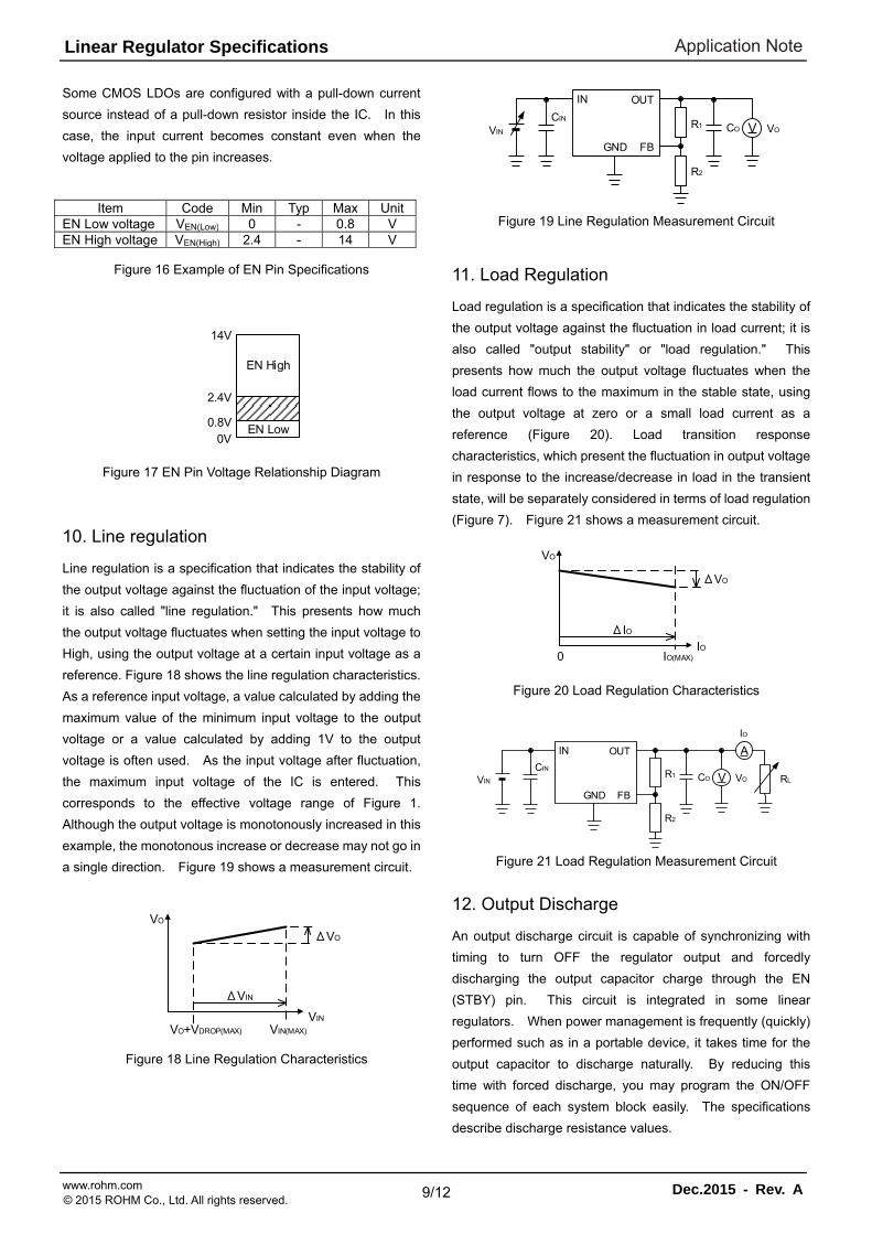
10. Line regulation
Line regulation is a specification that indicates the stability of
the output voltage against the fluctuation of the input voltage;
it is also called "line regulation." This presents how much
the output voltage fluctuates when setting the input voltage to
High, using the output voltage at a certain input voltage as a
reference. Figure 18 shows the line regulation characteristics.
As a reference input voltage, a value calculated by adding the
maximum value of the minimum input voltage to the output
voltage or a value calculated by adding 1V to the output
voltage is often used. As the input voltage after fluctuation,
the maximum input voltage of the IC is entered. This
corresponds to the effective voltage range of Figure 1.
Although the output voltage is monotonously increased in this
example, the monotonous increase or decrease may not go in
a single direction. Figure 19 shows a measurement circuit.
VO+VDROP(MAX) VIN(MAX)
VO
VIN
ΔVO
ΔVIN
Figure 18 Line Regulation Characteristics
IN OUT
FBGND
VIN VO
CIN
COR1
R2
V
Figure 19 Line Regulation Measurement Circuit
11. Load Regulation
Load regulation is a specification that indicates the stability of
the output voltage against the fluctuation in load current; it is
also called "output stability" or "load regulation." This
presents how much the output voltage fluctuates when the
load current flows to the maximum in the stable state, using
the output voltage at zero or a small load current as a
reference (Figure 20). Load transition response
characteristics, which present the fluctuation in output voltage
in response to the increase/decrease in load in the transient
state, will be separately considered in terms of load regulation
(Figure 7). Figure 21 shows a measurement circuit.
0 IO(MAX)
VO
IO
ΔVO
ΔIO
Figure 20 Load Regulation Characteristics
IN OUT
FBGND
VIN VO
CIN
COR1
R2
V
A
IO
RL
Figure 21 Load Regulation Measurement Circuit
12. Output Discharge
An output discharge circuit is capable of synchronizing with
timing to turn OFF the regulator output and forcedly
discharging the output capacitor charge through the EN
(STBY) pin. This circuit is integrated in some linear
regulators. When power management is frequently (quickly)
performed such as in a portable device, it takes time for the
output capacitor to discharge naturally. By reducing this
time with forced discharge, you may program the ON/OFF
sequence of each system block easily. The specifications
describe discharge resistance values.
Page 10
Application Note
10/12 www.rohm.com Dec.2015 - Rev. A© 2015 ROHM Co., Ltd. All rights reserved.
Linear Regulator Specifications
To activate this function, voltage must be always supplied to
the IC VIN pin and the output must be controlled through the
EN (STBY) pin. By controlling output ON/OFF using the
voltage from the VIN pin, the voltage turns OFF on the VIN
pin and the power supply to the output discharge circuit.
Accordingly, this function is disabled, thus causing natural
discharge.
Figure 22 shows the IC characteristics without output
discharge. Figure 23 shows the IC characteristics with
output discharge. In this example, the discharge speed is
8,000 times faster.
Figure 22 IC Characteristics without Output Discharge
Figure 23 IC Characteristics with Output Discharge
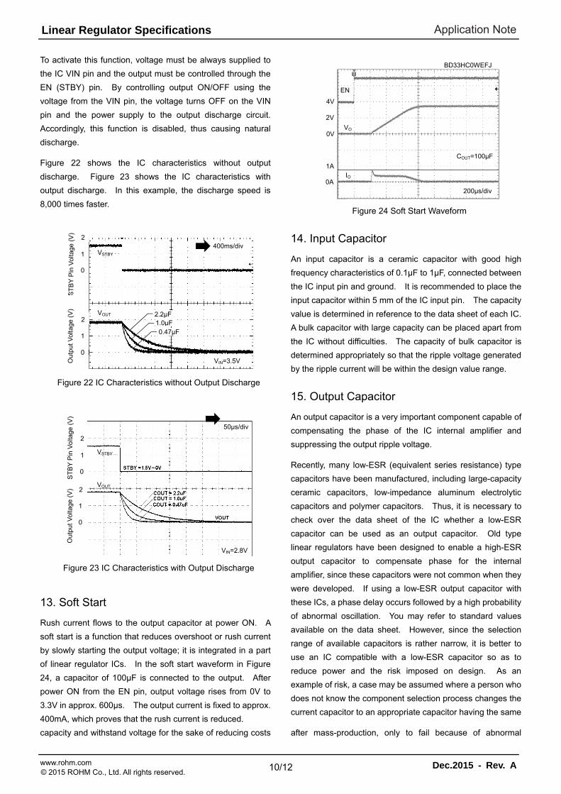
13. Soft Start
Rush current flows to the output capacitor at power ON. A
soft start is a function that reduces overshoot or rush current
by slowly starting the output voltage; it is integrated in a part
of linear regulator ICs. In the soft start waveform in Figure
24, a capacitor of 100μF is connected to the output. After
power ON from the EN pin, output voltage rises from 0V to
3.3V in approx. 600μs. The output current is fixed to approx.
400mA, which proves that the rush current is reduced.
Figure 24 Soft Start Waveform
14. Input Capacitor
An input capacitor is a ceramic capacitor with good high
frequency characteristics of 0.1μF to 1μF, connected between
the IC input pin and ground. It is recommended to place the
input capacitor within 5 mm of the IC input pin. The capacity
value is determined in reference to the data sheet of each IC.
A bulk capacitor with large capacity can be placed apart from
the IC without difficulties. The capacity of bulk capacitor is
determined appropriately so that the ripple voltage generated
by the ripple current will be within the design value range.
15. Output Capacitor
An output capacitor is a very important component capable of
compensating the phase of the IC internal amplifier and
suppressing the output ripple voltage.
Recently, many low-ESR (equivalent series resistance) type
capacitors have been manufactured, including large-capacity
ceramic capacitors, low-impedance aluminum electrolytic
capacitors and polymer capacitors. Thus, it is necessary to
check over the data sheet of the IC whether a low-ESR
capacitor can be used as an output capacitor. Old type
linear regulators have been designed to enable a high-ESR
output capacitor to compensate phase for the internal
amplifier, since these capacitors were not common when they
were developed. If using a low-ESR output capacitor with
these ICs, a phase delay occurs followed by a high probability
of abnormal oscillation. You may refer to standard values
available on the data sheet. However, since the selection
range of available capacitors is rather narrow, it is better to
use an IC compatible with a low-ESR capacitor so as to
reduce power and the risk imposed on design. As an
example of risk, a case may be assumed where a person who
does not know the component selection process changes the
current capacitor to an appropriate capacitor having the same
capacity and withstand voltage for the sake of reducing costs after mass-production, only to fail because of abnormal
ST
BY
Pin
Vol
tage
(V
) O
utpu
t Vol
tage
(V
)
0
1
2
0
1
2 VOUT
VSTBY
2.2μF1.0μF0.47μF
400ms/div
VIN=3.5V
0
1
2
0
1
2
Out
put V
olta
ge (
V)
ST
BY
Pin
Vol
tage
(V
)
VSTBY
VOUT
50μs/div
VIN=2.8V
0A
1A
0V
2V
4V
VO
IO
EN
200μs/div
BD33HC0WEFJ
COUT=100μF
Page 11
Application Note
11/12 www.rohm.com Dec.2015 - Rev. A© 2015 ROHM Co., Ltd. All rights reserved.
Linear Regulator Specifications
oscillation.
If the minimum capacity value is described in the data sheet,
that value is used as a standard. However, when the ripple
current is large or large current flows transiently, the ripple
voltage may not be within the design value range. In this
case, the capacity value should be increased as appropriate,
although power supply rise/fall become slow. When using
the minimum capacity value, due consideration must be given
to temperature characteristics, DC bias characteristics and
deterioration of capacity due to tolerance. Otherwise, the IC
may possibly oscillate. It is necessary to select a capacitor
based on a good understanding of the characteristics of each
capacitor; for example, an electrolytic capacitor is subject to
severer capacity deterioration at low temperature and a
ceramic capacitor is subject to capacity deterioration due to
DC bias.
16. Power Dissipation
As a linear regulator is subject to large power loss under
certain conditions, the package power dissipation is an
important item to judge the applicable range. However, it is
necessary to calculate the power loss from the input/output
voltage difference and output current, and make sure that the
chip temperature will not exceed the absolute maximum
rating of the junction temperature, using the package surface
temperature, in reference to the package thermal
characteristic parameter (thermal resistance).
The specifications may describe various numeric values for
the type of package. This is because the power dissipation
varies by the substrate type (difference in the number of
layers and copper foil area) in the case of surface mounted
packages that radiate heat to the substrate. The chip
temperature is estimated using the power dissipation data
close to that of the substrate to be actually used.
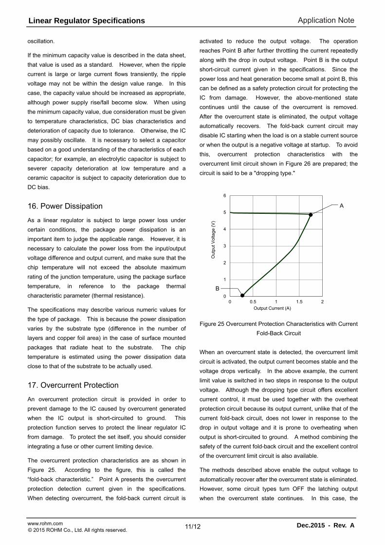
17. Overcurrent Protection
An overcurrent protection circuit is provided in order to
prevent damage to the IC caused by overcurrent generated
when the IC output is short-circuited to ground. This
protection function serves to protect the linear regulator IC
from damage. To protect the set itself, you should consider
integrating a fuse or other current limiting device.
The overcurrent protection characteristics are as shown in
Figure 25. According to the figure, this is called the
“fold-back characteristic.” Point A presents the overcurrent
protection detection current given in the specifications.
When detecting overcurrent, the fold-back current circuit is
activated to reduce the output voltage. The operation
reaches Point B after further throttling the current repeatedly
along with the drop in output voltage. Point B is the output
short-circuit current given in the specifications. Since the
power loss and heat generation become small at point B, this
can be defined as a safety protection circuit for protecting the
IC from damage. However, the above-mentioned state
continues until the cause of the overcurrent is removed.
After the overcurrent state is eliminated, the output voltage
automatically recovers. The fold-back current circuit may
disable IC starting when the load is on a stable current source
or when the output is a negative voltage at startup. To avoid
this, overcurrent protection characteristics with the
overcurrent limit circuit shown in Figure 26 are prepared; the
circuit is said to be a "dropping type."
Figure 25 Overcurrent Protection Characteristics with Current
Fold-Back Circuit
When an overcurrent state is detected, the overcurrent limit
circuit is activated, the output current becomes stable and the
voltage drops vertically. In the above example, the current
limit value is switched in two steps in response to the output
voltage. Although the dropping type circuit offers excellent
current control, it must be used together with the overheat
protection circuit because its output current, unlike that of the
current fold-back circuit, does not lower in response to the
drop in output voltage and it is prone to overheating when
output is short-circuited to ground. A method combining the
safety of the current fold-back circuit and the excellent control
of the overcurrent limit circuit is also available.
The methods described above enable the output voltage to
automatically recover after the overcurrent state is eliminated.
However, some circuit types turn OFF the latching output
when the overcurrent state continues. In this case, the
0
1
2
3
4
5
6
0 0.5 1 1.5 2
Out
put V
olta
ge (
V)
Output Current (A)
A
B
Page 12
Application Note
12/12 www.rohm.com Dec.2015 - Rev. A© 2015 ROHM Co., Ltd. All rights reserved.
Linear Regulator Specifications
output stays OFF after the overcurrent state is eliminated and
does not recover until the IC power is turned ON again.
Thus, it is necessary to check whether your IC is of
auto-recovery type or latch type on the data sheet.
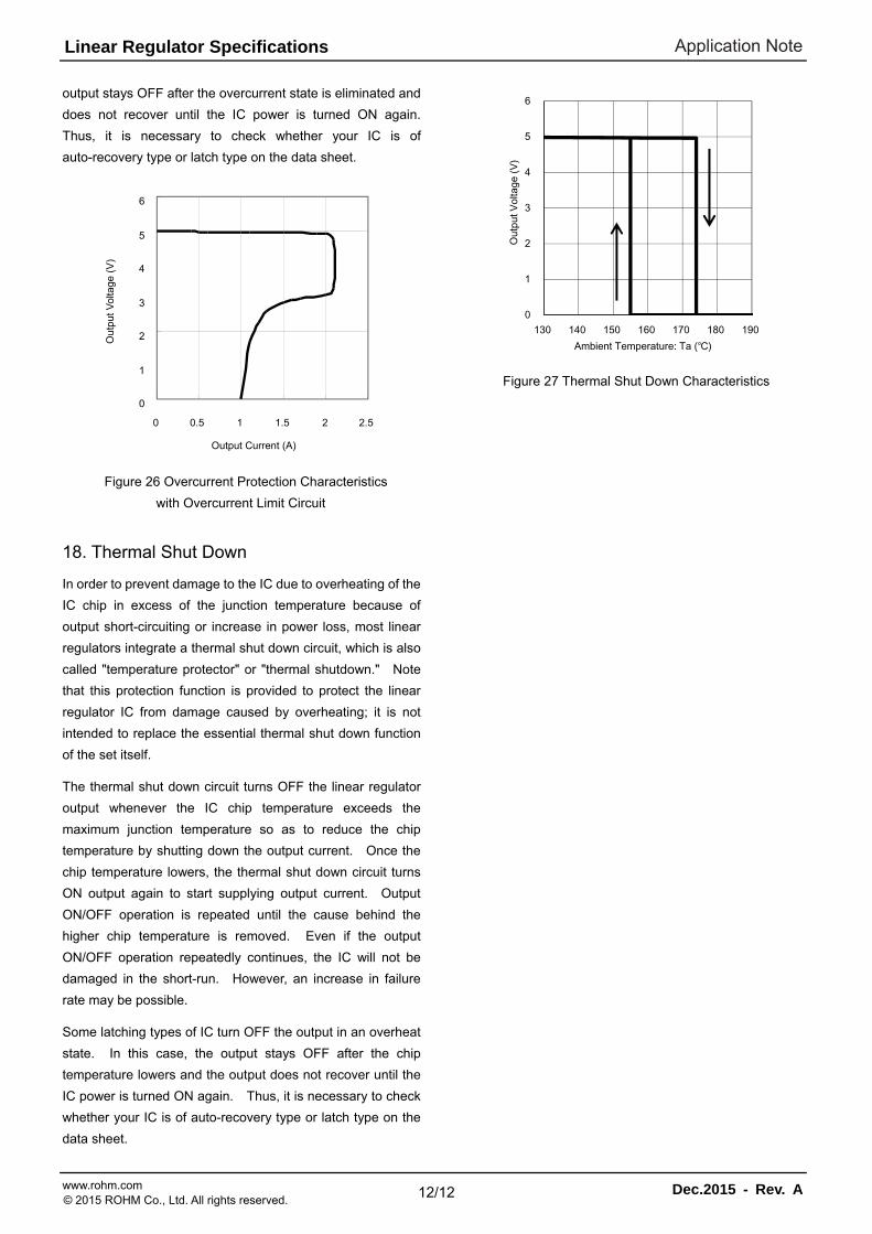
18. Thermal Shut Down
In order to prevent damage to the IC due to overheating of the
IC chip in excess of the junction temperature because of
output short-circuiting or increase in power loss, most linear
regulators integrate a thermal shut down circuit, which is also
called "temperature protector" or "thermal shutdown." Note
that this protection function is provided to protect the linear
regulator IC from damage caused by overheating; it is not
intended to replace the essential thermal shut down function
of the set itself.
The thermal shut down circuit turns OFF the linear regulator
output whenever the IC chip temperature exceeds the
maximum junction temperature so as to reduce the chip
temperature by shutting down the output current. Once the
chip temperature lowers, the thermal shut down circuit turns
ON output again to start supplying output current. Output
ON/OFF operation is repeated until the cause behind the
higher chip temperature is removed. Even if the output
ON/OFF operation repeatedly continues, the IC will not be
damaged in the short-run. However, an increase in failure
rate may be possible.
Some latching types of IC turn OFF the output in an overheat
state. In this case, the output stays OFF after the chip
temperature lowers and the output does not recover until the
IC power is turned ON again. Thus, it is necessary to check
whether your IC is of auto-recovery type or latch type on the
data sheet.
Figure 27 Thermal Shut Down Characteristics
0
1
2
3
4
5
6
130 140 150 160 170 180 190
Out
put V
olta
ge (V
)
Ambient Temperature: Ta ()
0
1
2
3
4
5
6
0 0.5 1 1.5 2 2.5
Output Current (A)
Out
put V
olta
ge (
V)
Figure 26 Overcurrent Protection Characteristics
with Overcurrent Limit Circuit
Page 13
R1102Awww.rohm.com© 2015 ROHM Co., Ltd. All rights reserved.
Notice
ROHM Customer Support System http://www.rohm.com/contact/
Thank you for your accessing to ROHM product informations. More detail product informations and catalogs are available, please contact us.
N o t e s
The information contained herein is subject to change without notice.
Before you use our Products, please contact our sales representative and verify the latest specifica-tions :
Although ROHM is continuously working to improve product reliability and quality, semicon-ductors can break down and malfunction due to various factors.Therefore, in order to prevent personal injury or fire arising from failure, please take safety measures such as complying with the derating characteristics, implementing redundant and fire prevention designs, and utilizing backups and fail-safe procedures. ROHM shall have no responsibility for any damages arising out of the use of our Poducts beyond the rating specified by ROHM.
Examples of application circuits, circuit constants and any other information contained herein are provided only to illustrate the standard usage and operations of the Products. The peripheral conditions must be taken into account when designing circuits for mass production.
The technical information specified herein is intended only to show the typical functions of and examples of application circuits for the Products. ROHM does not grant you, explicitly or implicitly, any license to use or exercise intellectual property or other rights held by ROHM or any other parties. ROHM shall have no responsibility whatsoever for any dispute arising out of the use of such technical information.
The Products are intended for use in general electronic equipment (i.e. AV/OA devices, communi-cation, consumer systems, gaming/entertainment sets) as well as the applications indicated in this document.
The Products specified in this document are not designed to be radiation tolerant.
For use of our Products in applications requiring a high degree of reliability (as exemplified below), please contact and consult with a ROHM representative : transportation equipment (i.e. cars, ships, trains), primary communication equipment, traffic lights, fire/crime prevention, safety equipment, medical systems, servers, solar cells, and power transmission systems.
Do not use our Products in applications requiring extremely high reliability, such as aerospace equipment, nuclear power control systems, and submarine repeaters.
ROHM shall have no responsibility for any damages or injury arising from non-compliance with the recommended usage conditions and specifications contained herein.
ROHM has used reasonable care to ensur the accuracy of the information contained in this document. However, ROHM does not warrants that such information is error-free, and ROHM shall have no responsibility for any damages arising from any inaccuracy or misprint of such information.
Please use the Products in accordance with any applicable environmental laws and regulations, such as the RoHS Directive. For more details, including RoHS compatibility, please contact a ROHM sales office. ROHM shall have no responsibility for any damages or losses resulting non-compliance with any applicable laws or regulations.
When providing our Products and technologies contained in this document to other countries, you must abide by the procedures and provisions stipulated in all applicable export laws and regulations, including without limitation the US Export Administration Regulations and the Foreign Exchange and Foreign Trade Act.
This document, in part or in whole, may not be reprinted or reproduced without prior consent of ROHM.
1)
2)
3)
4)
5)
6)
7)
8)
9)
10)
11)
12)
13)
14)