76
Linearization Techniques for CMOS LNAs: A Tutorial Edgar Sánchez-Sinencio Analog and Mixed Signal Center
Linearization Techniques for CMOS LNAs: A Tutorial
Edgar Sánchez-Sinencio
Analog and Mixed Signal Center

2
Outline
• Motivation
• Linearization Techniques
• New Issues for Wideband Applications
• LNA Linearization in Deep Submicron Process
• Remarks for High Linearity LNA Design
3
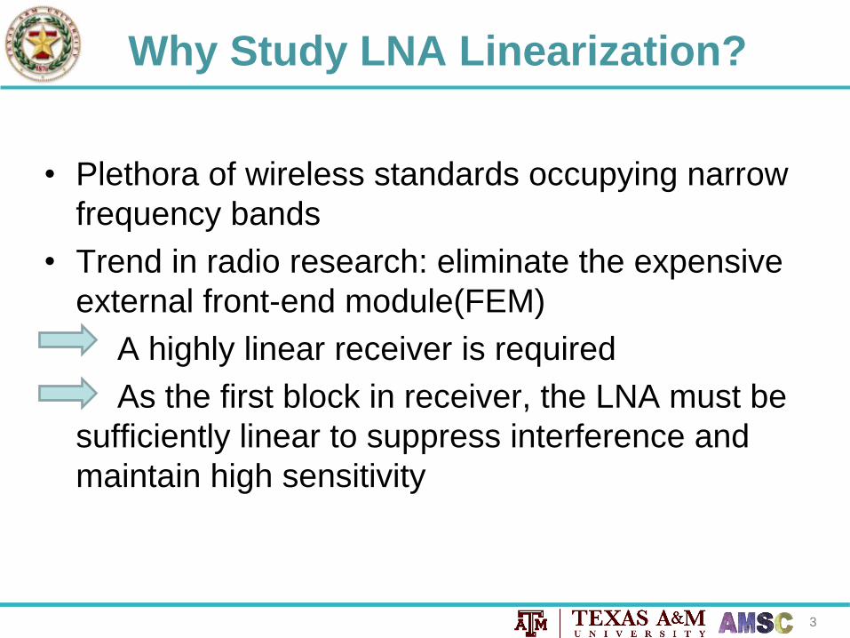
Why Study LNA Linearization?
• Plethora of wireless standards occupying narrow
frequency bands
• Trend in radio research: eliminate the expensive
external front-end module(FEM)
A highly linear receiver is required
As the first block in receiver, the LNA must be
sufficiently linear to suppress interference and
maintain high sensitivity
4
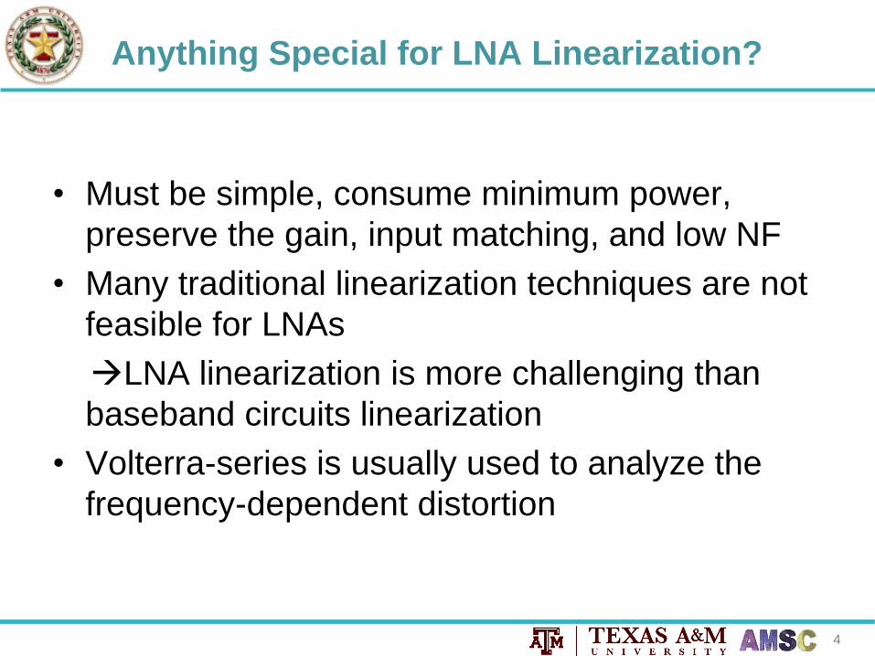
Anything Special for LNA Linearization?
• Must be simple, consume minimum power,
preserve the gain, input matching, and low NF
• Many traditional linearization techniques are not
feasible for LNAs
LNA linearization is more challenging than
baseband circuits linearization
• Volterra-series is usually used to analyze the
frequency-dependent distortion

5
LNA Linearization Techniques
• A weakly nonlinear amplifier is characterized by:
• Goal of linearization: make g2,3 small
enough to be negligible, hence
• Two distortion sources for LNA:
– Nonlinear transconductance gm , “input limited”
– Nonlinear output conductance gds , “output limited”
2 3
1 2 3Y g X g X g X
X: input; Y:output; g1,2,3 : linear gain/second/third-order nonlinearity coefficients
1Y g X
6
Outline
• Motivation
• Linearization Techniques
• New Issues for Wideband Applications
• LNA Linearization in Deep Submicron Process
• Remarks for High Linearity LNA Design
7
LNA Linearization Techniques
• Eight categories for the sake of discussion:
– a) Feedback
– b) Harmonic termination
– c) Optimum biasing
– d) Feedforward
– e) Derivative superposition(DS)
– f) IM2 injection
– g) Noise/distortion cancellation
– h) Post-distortion

8
Distortion Sources & Corresponding
Linearization Methods
Distortion
Sources
Linearization
Methods
gm gds
Intrinsic
2nd-order
Intrinsic
3rd-order
2nd-order
interaction
Intrinsic
Higher order
Feedback √ √ √ √
Harmonic termination √ √
Optimal biasing √
Feedforward √ √ √
Derivative
superposition(DS)
√
Complementary DS √ √
Differential DS √ √
Modified DS √ √
IM2 injection √ √
Noise/distortion
cancellation
√ √ √
Post-distortion √ √

9
LNA Linearization Techniques
• Eight categories:
– a) Feedback
– b) Harmonic termination
– c) Optimum biasing
– d) Feedforward
– e) Derivative superposition(DS)
– f) IM2 injection
– g) Noise/distortion cancellation
– h) Post-distortion
10
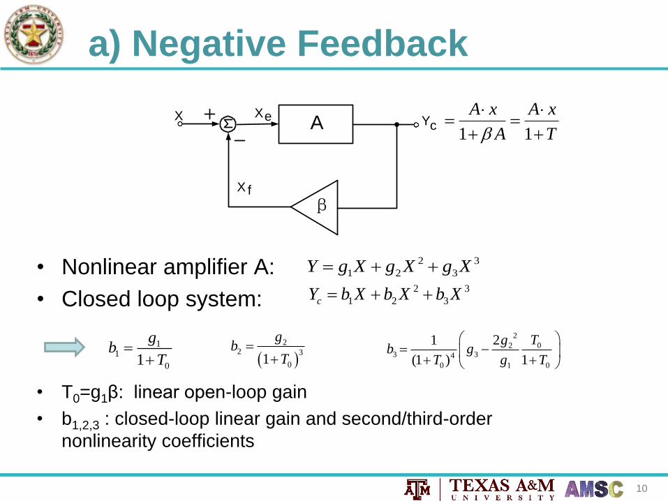
a) Negative Feedback
• Nonlinear amplifier A:
• Closed loop system:
• T0=g1β: linear open-loop gain
• b1,2,3 : closed-loop linear gain and second/third-order
nonlinearity coefficients
AXeX Y
βX f
c
2 3
1 2 3Y g X g X g X
2 3
1 2 3cY b X b X b X
11
01
gb
T
2
2 3
01
gb
T
2
023 34
0 1 0
21
(1 ) 1
Tgb g
T g T
1 1
A x A x
A T

11
a) Negative Feedback
• IIP2 of the open-loop amplifier A:
• IIP2 of the closed-loop system:
• IIP3 of the open-loop amplifier A:
• IIP3 of the closed-loop system:
• Negative feedback improves AIIP2 by a factor of (1+T0); improves AIIP3
by a factor of (1+T0)3/2 when g2 ≈ 0;
• Nonzero g2 degrades IIP3 when g1 and g3 have opposite signs
“2nd-order interaction”
12,
2
IIP amplifier
gA
g
21 1
2,
2 2
1IIP closeloop o
b gA T
b g
13,
3
4
3IIP amplifier
gA
g
3
1 13, 2
3 3 2
1 3
14 4
3 3 21
1
o
IIP closeloop
o
o
Tb gA
b g Tg
g g T

12
a) Negative Feedback: Example
g1vgs
G
Cgs
S
D
g2vgs2
2 1
1 2
1 22 ,2
Y = id
ß = Ls
Xf = Vs
X = Vin
+
-
Xe = Vgs
g3vgs3
1 2,
Ls : frequency-dependent feedback element; β=ωLs feedback path between id & vin.
Inductively source-degenerated LNA:
2 3
1 2 3d in s in s in si g v v g v v g v v
vs ≠ 0, and contains components 2ω1, 2ω2, and ω1 + ω2 due to the 2nd-order distortion
the product term -2g2vinvs from g2(vin-vs)2 generates IM3 terms 2ω1+ω2 and 2ω2+ω1.
the intrinsic 2nd-order nonlinearity contributes to 3rd-order intermodulation, IM3, when a
feedback mechanism is employed.
13
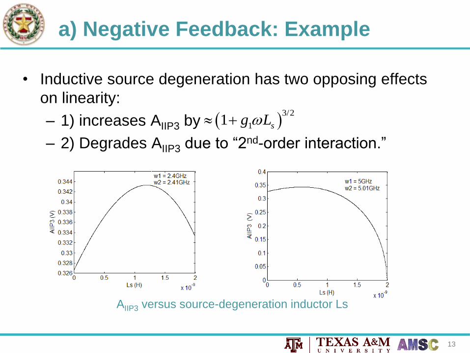
a) Negative Feedback: Example
• Inductive source degeneration has two opposing effects
on linearity:
– 1) increases AIIP3 by
– 2) Degrades AIIP3 due to “2nd-order interaction.”
3/2
11 sg L
AIIP3 versus source-degeneration inductor Ls

14
a) Negative Feedback: Limitations
• Two sources for the 3rd-order nonlinearity of an
amplifier in feedback: – intrinsic amplifier 3rd-order nonlinearity.
– “2nd-order interaction” (from intrinsic 2nd-order nonlinearity
combined with feedback).
• Feedback for LNAs is not as effective as for
baseband circuits because: – the open loop gain T0 cannot be large due to stringent LNA gain,
noise, and power requirement.
– the 2nd-order nonlinearity contributes to the IM3 indirectly
through “2nd-order interaction.”

15
LNA Linearization Techniques
• Eight categories:
– a) Feedback
– b) Harmonic termination
– c) Optimum biasing
– d) Feedforward
– e) Derivative superposition(DS)
– f) IM2 injection
– g) Noise/distortion cancellation
– h) Post-distortion
16
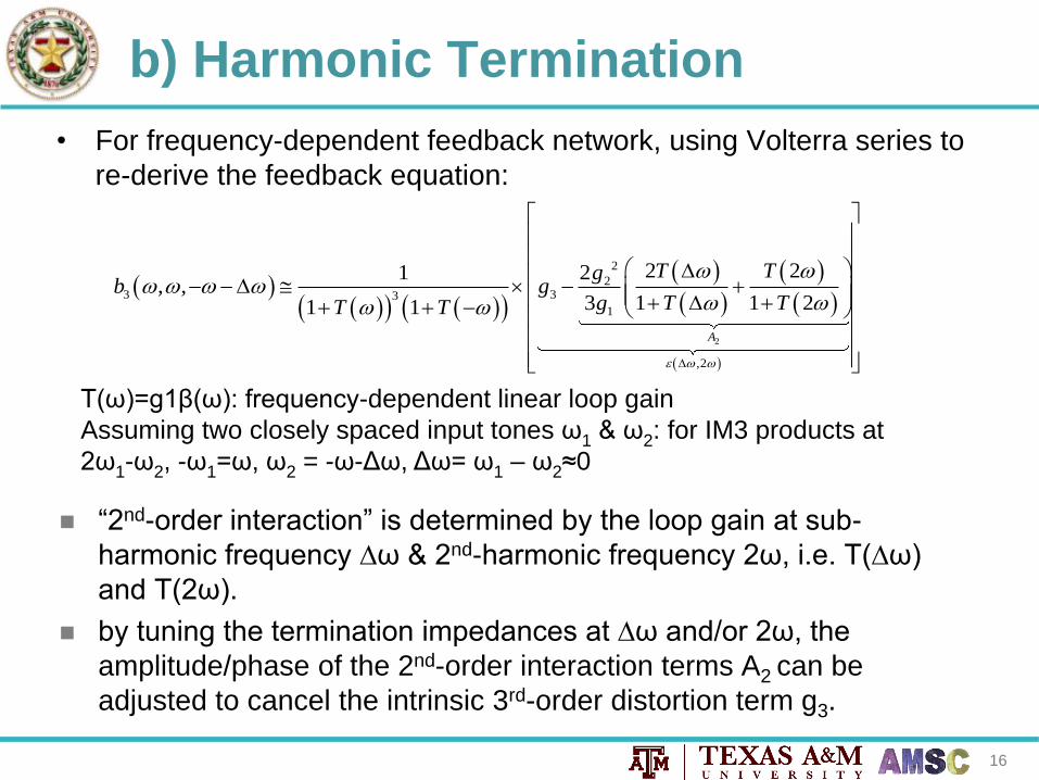
b) Harmonic Termination
• For frequency-dependent feedback network, using Volterra series to
re-derive the feedback equation:
T(ω)=g1β(ω): frequency-dependent linear loop gain
Assuming two closely spaced input tones ω1 & ω2: for IM3 products at
2ω1-ω2, -ω1=ω, ω2 = -ω-Δω, Δω= ω1 – ω2≈0
2
2
23 33
1
,2
2 221, ,
3 1 1 21 1
A
T Tgb g
g T TT T
“2nd-order interaction” is determined by the loop gain at sub-
harmonic frequency ∆ω & 2nd-harmonic frequency 2ω, i.e. T(∆ω)
and T(2ω).
by tuning the termination impedances at ∆ω and/or 2ω, the
amplitude/phase of the 2nd-order interaction terms A2 can be
adjusted to cancel the intrinsic 3rd-order distortion term g3.
17
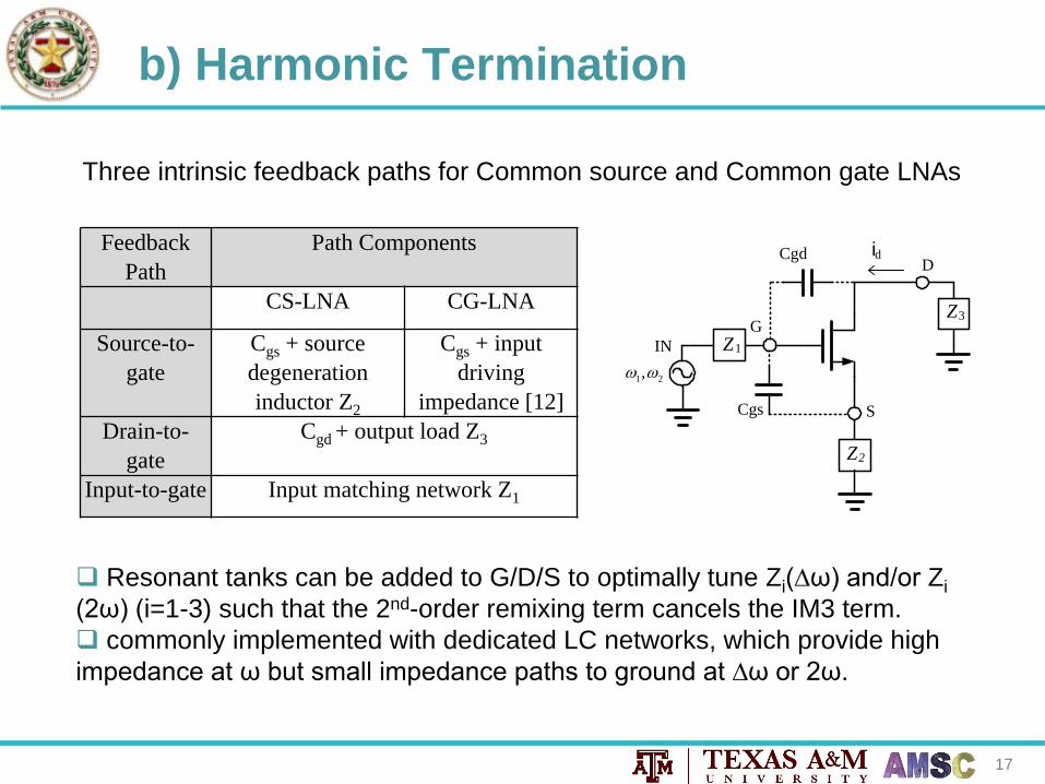
b) Harmonic Termination
Feedback
Path
Path Components
CS-LNA CG-LNA
Source-to-
gate
Cgs + source
degeneration
inductor Z2
Cgs + input
driving
impedance [12]
Drain-to-
gate
Cgd + output load Z3
Input-to-gate Input matching network Z1
Z1
G
S
Did
Z3
Z2
1 2,
Cgs
Cgd
IN
Three intrinsic feedback paths for Common source and Common gate LNAs
Resonant tanks can be added to G/D/S to optimally tune Zi(∆ω) and/or Zi
(2ω) (i=1-3) such that the 2nd-order remixing term cancels the IM3 term.
commonly implemented with dedicated LC networks, which provide high
impedance at ω but small impedance paths to ground at ∆ω or 2ω.
18
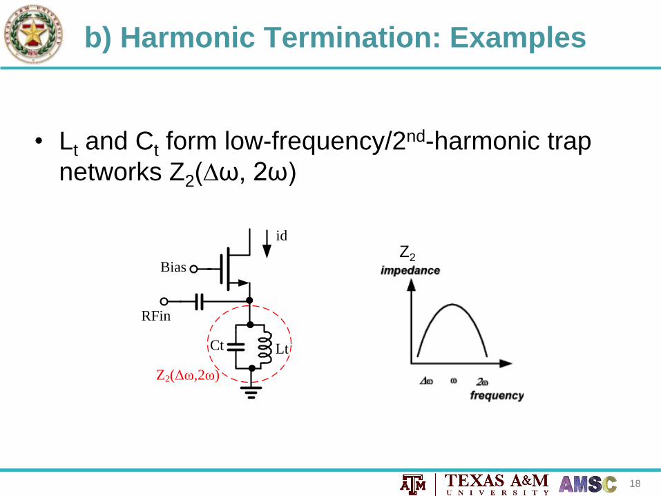
b) Harmonic Termination: Examples
• Lt and Ct form low-frequency/2nd-harmonic trap
networks Z2(∆ω, 2ω)
Bias
RFin
LtCt
id
Z2(Δω,2ω)
Z2

19
b) Harmonic Termination: Limitations
• Harmonic termination only works well in
narrowband systems because the tuning
network is optimized at Δω and 2ω
• only works for a narrow range of two
tone spacing/center frequencies [9].
• For wideband applications, Δω and 2ω vary
considerablydifficult to tune out the termination
impedance.

20
LNA Linearization Techniques
• Eight categories:
– a) Feedback
– b) Harmonic termination
– c) Optimum biasing
– d) Feedforward
– e) Derivative superposition(DS)
– f) IM2 injection
– g) Noise/distortion cancellation
– h) Post-distortion

21
c) Optimal Biasing
• To characterize the single-transistor nonlinearity, we fixed its Vds,
swept the Vgs, and then took the first three derivatives of Ids with
respect to Vgs at every DC bias point to obtain these plots:
NMOS transconductance characteristics
(UMC 90nm CMOS process, W/L = 20/0.08μm, Vds = 1V).
22
c) Optimal Biasing: Limitations
• Sensitive to PVT
• limited input-signal amplitude range for effective distortion
cancellation.
• A single transistor characteristic and only signifies optimum
intrinsic 3rd-order gm nonlinearity; “sweet spot” is
frequency-dependent, and the IIP3 peak decreases due to
parasitic effects
• Biasing the transistor at g3 = 0 restricts the input-stage
transconductance, lowering gain and increasing NF.
• Only works for fixed-gain LNAs(no AGC involved)
23
LNA Linearization Techniques
• Eight categories:
– a) Feedback
– b) Harmonic termination
– c) Optimum biasing
– d) Feedforward
– e) Derivative superposition(DS)
– f) IM2 injection
– g) Noise/distortion cancellation
– h) Post-distortion

24
d) Feedforward
• Cancellation of g2 and/or g3 with minimum effects
on g1 requires more degrees of freedom.
• generating additional nonlinear currents/voltages,
and subsequently summing (subtracting) them
accomplishes such cancellation.
• an auxiliary path includes a replica amplifier &
signal-scaling factors b &1/bn to replicate the
distortion in the main path.

25
d) Feedforward: example
Auxiliary
Amplifier
Main
Amplifier
X Y
main
Yauxiliary
b b
Y
Auxiliary Path
n
2 3
1 2 3mainY g X g X g X
2 3
1 2 3
1auxiliary n
Y g bX g bX g bXb
2 3
1 2 31 2 3
Residue Distortion
1 1 11 1 1main auxiliary n n n
Y Y Y g X g X g Xb b b
• gain-attenuation factor:
(1-1/bn-1), thus gain is
reduced by 2.5dB with
b = 2 and n = 3.
• only cancel one type of
harmonic at a time; to
reduce both 2nd- & 3rd-order
distortion simultaneously,
an additional degree of
freedom is required
two auxiliary paths

26
d) Feedforward: Limitations
• Accurate, noiseless, and highly linear scaling
factors are often not feasible.
• Additional active components introduce more noise.
• Highly sensitive to mismatch between the main and
auxiliary gain stages.
• Large power overhead due to the auxiliary
amplifier. In worst case, the auxiliary amplifier is an
exact copy of the main amplifierdouble the power
27
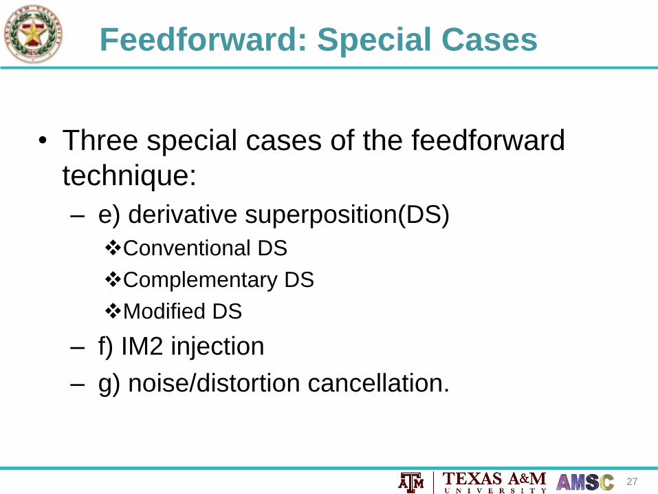
Feedforward: Special Cases
• Three special cases of the feedforward
technique:
– e) derivative superposition(DS)
Conventional DS
Complementary DS
Modified DS
– f) IM2 injection
– g) noise/distortion cancellation.
28
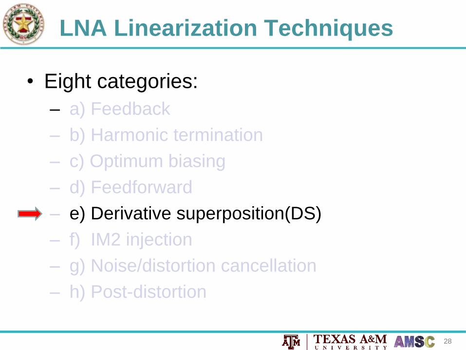
LNA Linearization Techniques
• Eight categories:
– a) Feedback
– b) Harmonic termination
– c) Optimum biasing
– d) Feedforward
– e) Derivative superposition(DS)
– f) IM2 injection
– g) Noise/distortion cancellation
– h) Post-distortion

29
e) Derivative Superposition (DS)
• A special case of the feedforward
technique: obtained when b=1 and the
main/auxiliary amplifiers are implemented
with transistors in different regions or types
• It adds the 3rd derivatives (g3) of drain
current from the main and auxiliary
transistors to cancel distortion.

30
e) Conventional DS
• Linearity is improved within a finite bias-voltage
range instead of just a point
MA
MB
ioutVaux
Vmain
IN Aux
transistor
31
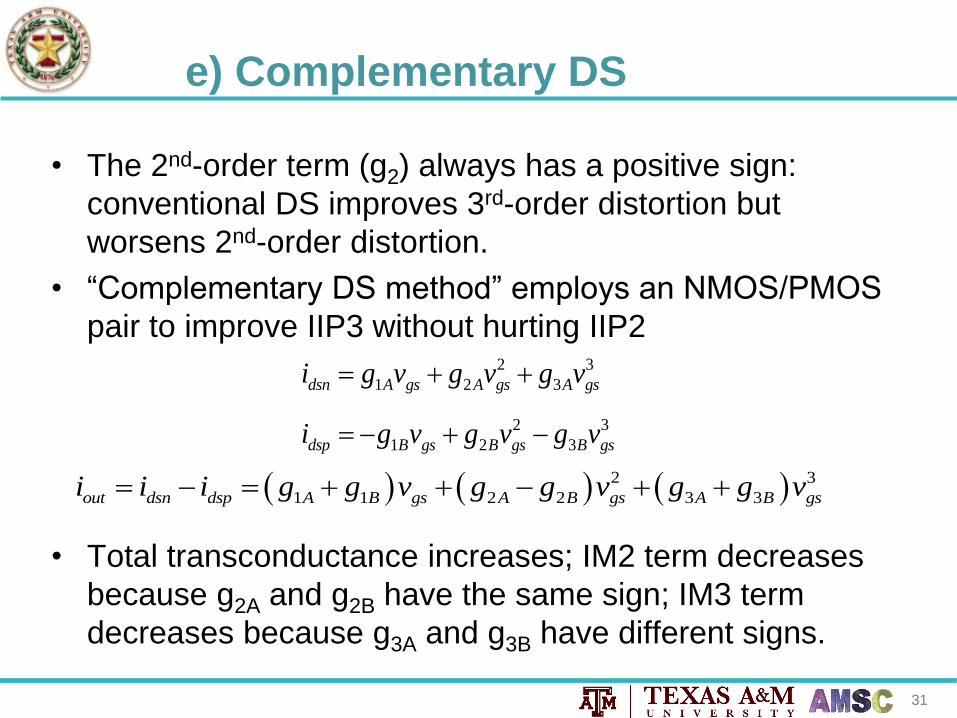
e) Complementary DS
• The 2nd-order term (g2) always has a positive sign:
conventional DS improves 3rd-order distortion but
worsens 2nd-order distortion.
• “Complementary DS method” employs an NMOS/PMOS
pair to improve IIP3 without hurting IIP2
• Total transconductance increases; IM2 term decreases
because g2A and g2B have the same sign; IM3 term
decreases because g3A and g3B have different signs.
2 3
1 2 3dsn A gs A gs A gsi g v g v g v
2 3
1 2 3dsp B gs B gs B gsi g v g v g v
2 3
1 1 2 2 3 3out dsn dsp A B gs A B gs A B gsi i i g g v g g v g g v

32
e) Complementary DS: Examples
Common-source configuration
MA
MB
idsn
Vaux
Vmain
INAux
transistor
VDD
idsp
iout
MA
MB
idsnVmain
IN
Aux
transistor
VDD
idsp
Vout
Vaux
AC
Current
Combiner
x
y
x
y
x
y
VDD
iout
Common-gate configuration

33
e) Complementary DS vs. Conventional DS
• g2 is maximized for conventional DS & minimized for complementary DS.
• the g3 cancellation window is narrower and less flat for complementary
DS since PMOS and NMOS devices have different linearity
characteristics.
Comparison of conventional (dual-NMOS) DS and complementary
(PMOS/NMOS) DS: (a) g2 vs. Vgs (b) g3 vs. Vgs (UMC 90nm CMOS process, Vds = 1V).

34
e) Modified DS
• Motivation: the “2nd-order interaction” ultimately
limits the IIP3 at higher frequencies, after the
intrinsic g3-induced 3rd-order distortion is
cancelled by the DS method.
• Three feedback paths exist for “2nd-order
interaction”: source-to-gate, drain-to-gate, and
input-to-gate.
• The modified DS methods minimize the source-
to-gate feedback reducing 2nd-order
interaction
35
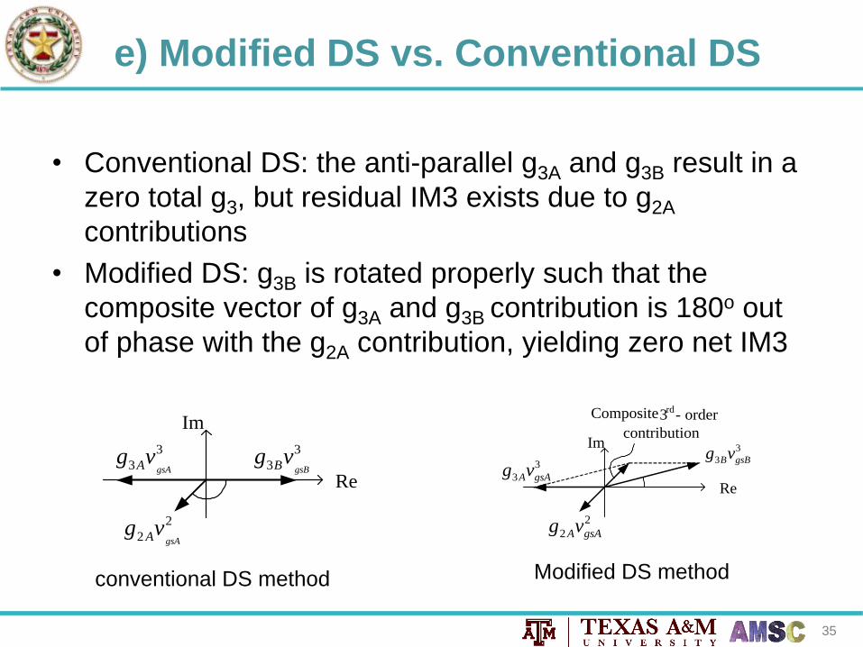
e) Modified DS vs. Conventional DS
• Conventional DS: the anti-parallel g3A and g3B result in a
zero total g3, but residual IM3 exists due to g2A
contributions
• Modified DS: g3B is rotated properly such that the
composite vector of g3A and g3B contribution is 180o out
of phase with the g2A contribution, yielding zero net IM3
Re
Im
3
3 gsAAg v 3
3 gsBBg v
2
2 gsAAg v
Re
Im
Composite 3rd
- order
contribution
3
3A gsAg v
3
3B gsBg v
2
2 A gsAg v
conventional DS method Modified DS method
36
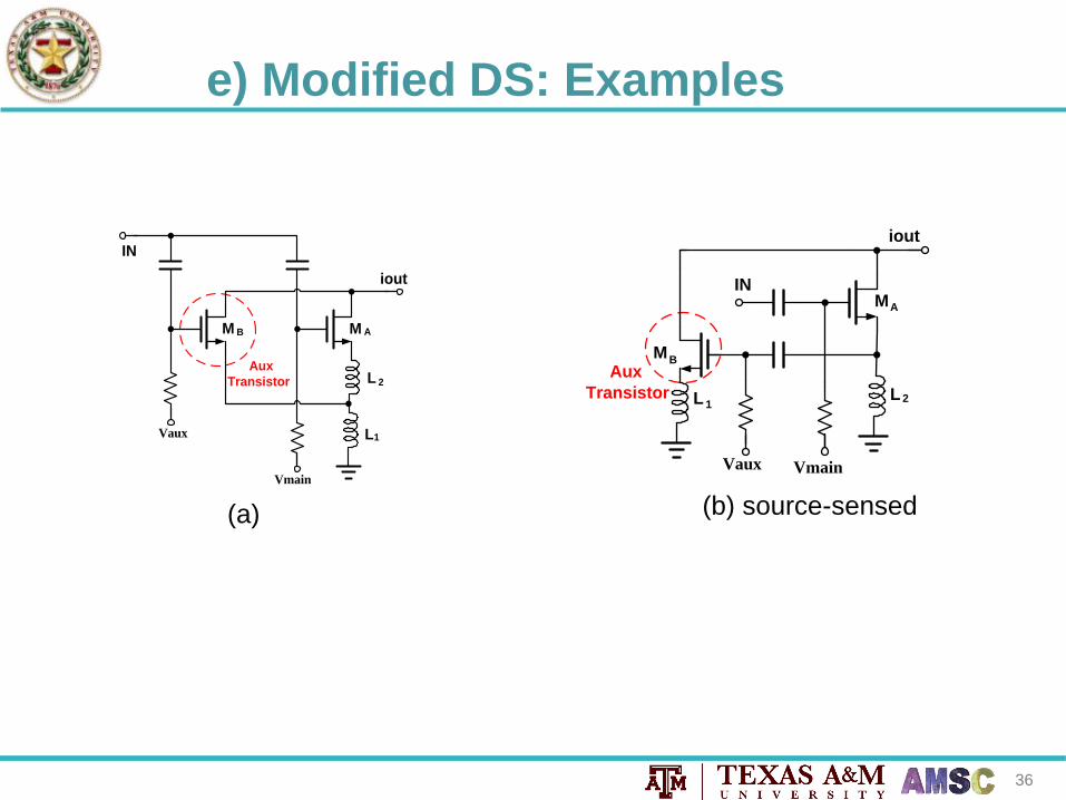
e) Modified DS: Examples
M B M A
iout
IN
L 2
L1
Aux
Transistor
Vaux
Vmain
MB
MA
iout
IN
L 2L 1
Aux
Transistor
Vaux Vmain
(a) (b) source-sensed

37
e) Modified DS: Limitations
• The weak-inversion transistor may not
operate at very high frequency; cannot
handle large signals or it will be turned off,
very limited distortion-cancellation
range.
• Weak-inversion transistor models are
generally not accurate discrepancy
between simulation & measurement.
• Matching transistors working in different
regions is difficult a linearity
improvement sensitive to PVT variations.
Measured IIP3 with/without DS method

38
LNA Linearization Techniques
• Eight categories:
– a) Feedback
– b) Harmonic termination
– c) Optimum biasing
– d) Feedforward
– e) Derivative superposition(DS)
– f) IM2 injection
– g) Noise/distortion cancellation
– h) Post-distortion

39
f) IM2 Injection
• Eliminates the explicit auxiliary path by merging
it with the main path to reuse the active devices
and the DC current
• Externally generates and injects a low-frequency
IM2 component into the circuit.
• Key idea: tune the amplitude & phase of the
injected IM2 current for optimal distortion
cancellation

40
f) IM2 Injection: Implementation
• M4, M5, R, and C compose
a squaring circuit to
generate a low-frequency
IM2 current at ω2 –ω1,
which is then injected
through M3 into the
common source node vs
• Design equation:
1 3 2 2 1, 3 2, 1
Main Circuit Squaring Circuit
(2 4 ) 3 2 2M Mg g g g g g R
41
f) IM2 Injection: Limitations
• NMOS/PMOS transistors and resistors have independent PVT
variations difficult to satisfy the IM3 cancellation criteria robustly.
• R and C in the IM2 generator introduce extra phase shift, two tone
spacing must be smaller than the RC-filter cutoff frequency for
negligible phase mismatch. Cancellation performance degrades as
tone spacing increases.
• Frequency components at ω2 +ω1 and 2ω1,2 injected by the IM2
generator may fall into signal band and degrade the IIP2.
• Noise from the IM2 generator is negligible only for differential LNAs,
• In short, IM2 injection applies chiefly to narrowband, differential
systems with small two-tone spacing.
42
LNA Linearization Techniques
• Eight categories:
– a) Feedback
– b) Harmonic termination
– c) Optimum biasing
– d) Feedforward
– e) Derivative superposition(DS)
– f) IM2 injection
– g) Noise/distortion cancellation
– h) Post-distortion

43
g) Noise/Distortion Cancellation
• Design equations:
1, 1,A BM A M Bg R g R 1 21, 1,B BM s M Ag R g R
(a) Differential output (b) Single-ended output

44
g) Noise/Distortion Cancellation
• Requirement: the two paths through MA and MB are
balanced for the noise/distortion current
• can cancel all intrinsic distortion generated by MA,
including both gm and gds nonlinearity
• Limitation: after cancelling the distortion from MA, MB’s
distortion dominates the residual nonlinearity, which
comprises two terms: 1) MB’s intrinsic 3rd-order distortion
and 2) 2nd-order interaction originating from the CG-CS
cascade.

45
LNA Linearization Techniques
• Eight categories:
– a) Feedback
– b) Harmonic termination
– c) Optimum biasing
– d) Feedforward
– e) Derivative superposition(DS)
– f) IM2 injection
– g) Noise/distortion cancellation
– h) Post-distortion
46
h) Post-Distortion(PD)
• Similar to the DS method, the PD method also uses
an auxiliary transistor’s nonlinearity to cancel that of
the main device, but it is more advanced in two
aspects:
– The auxiliary transistor is connected to the output of main
device, minimizing the impact on input matching.
– All transistors operate in saturation, resulting in more
robust distortion cancellation.
47
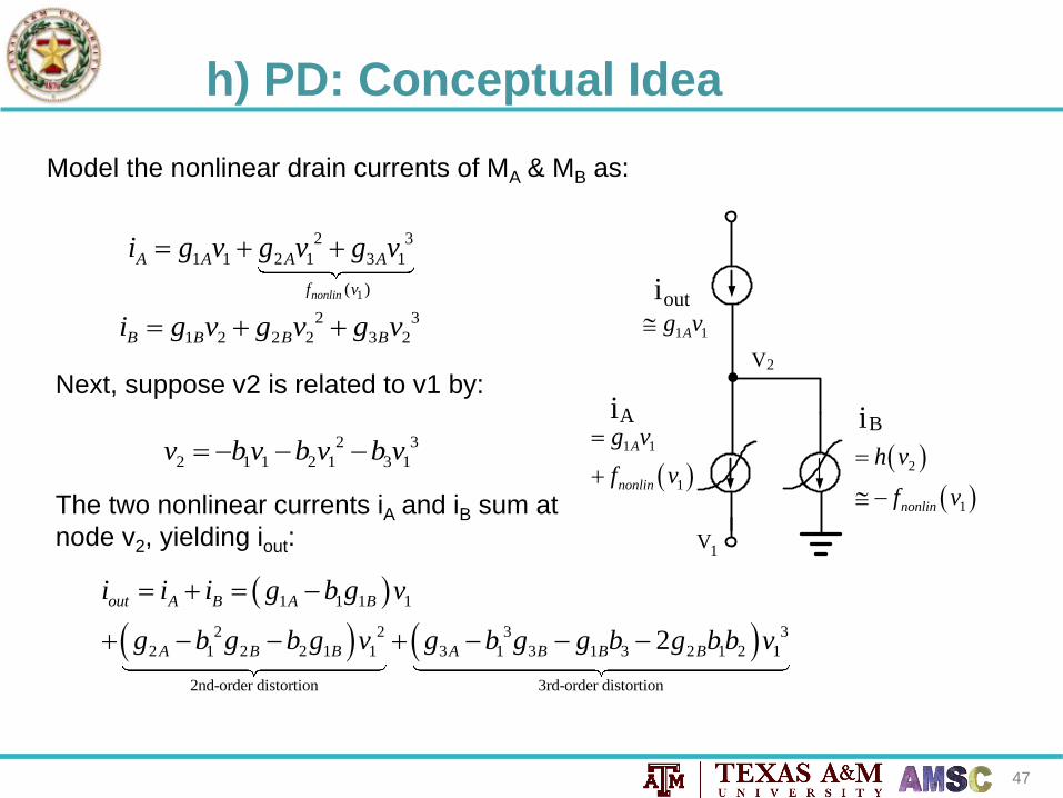
h) PD: Conceptual Idea
iA
iout
iB
V1
V2
1 1
1
A
nonlin
g v
f v
2
1nonlin
h v
f v
1 1Ag v
1
2 3
1 1 2 1 3 1
( )nonlin
A A A A
f v
i g v g v g v
2 3
1 2 2 2 3 2B B B Bi g v g v g v
Model the nonlinear drain currents of MA & MB as:
Next, suppose v2 is related to v1 by:
2 3
2 1 1 2 1 3 1v b v b v b v
1 1 1 1
2 2 3 3
2 1 2 2 1 1 3 1 3 1 3 2 1 2 1
2nd-order distortion 3rd-order distortion
2
out A B A B
A B B A B B B
i i i g b g v
g b g b g v g b g g b g b b v
The two nonlinear currents iA and iB sum at
node v2, yielding iout:
48
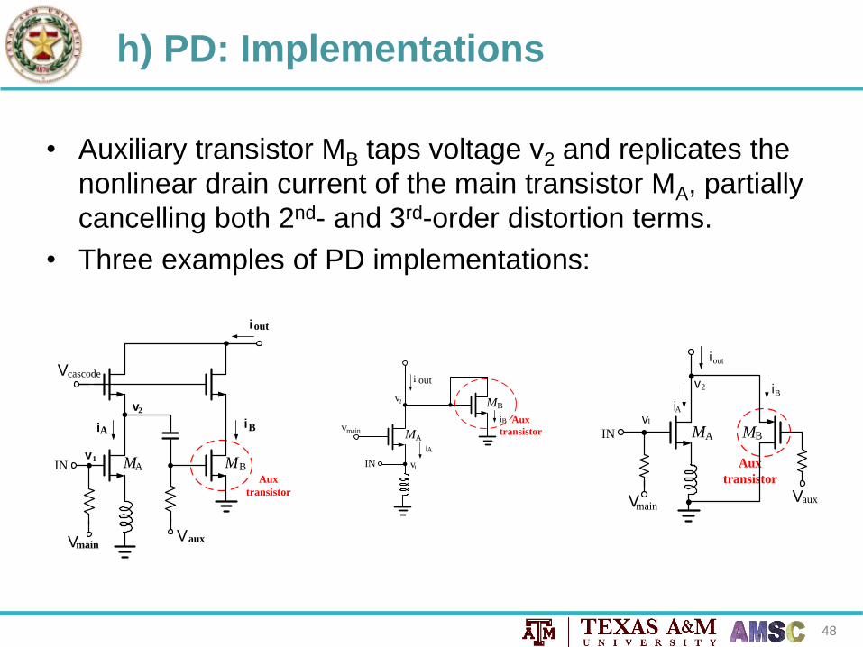
h) PD: Implementations
• Auxiliary transistor MB taps voltage v2 and replicates the
nonlinear drain current of the main transistor MA, partially
cancelling both 2nd- and 3rd-order distortion terms.
• Three examples of PD implementations:
MAIN
Vcascode
iAiB
iout
v1
v2
Aux
transistor
MB
VmainVaux
IN
Vmain
iA
iB
iout
v1
Vaux
v2
MA MB
Aux
transistor
mainV
iA
i out
Bi
v2
v1
MA
MB
IN
Aux
transistor

49
Distortion Sources & Corresponding
Linearization Methods
Distortion
Sources
Linearization
Methods
gm gds
Intrinsic
2nd-order
Intrinsic
3rd-order
2nd-order
interaction
Higher
order
Feedback √ √ √ √
Harmonic termination √ √
Optimal biasing √
Feedforward √ √ √
Derivative
superposition(DS)
√
Complementary DS √ √
Differential DS √ √
Modified DS √ √
IM2 injection √ √
Noise/distortion
cancellation
√ √ √
Post-distortion √ √
50
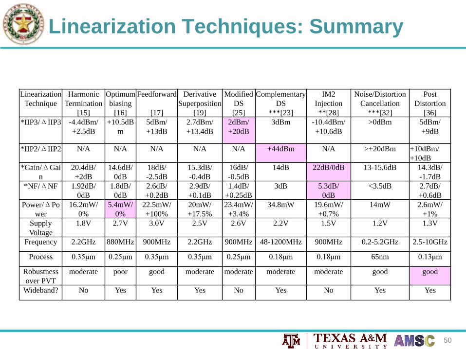
Linearization Techniques: Summary
Linearization
Technique
Harmonic
Termination
[15]
Optimum
biasing
[16]
Feedforward
[17]
Derivative
Superposition
[19]
Modified
DS
[25]
Complementary
DS
***[23]
IM2
Injection
**[28]
Noise/Distortion
Cancellation
***[32]
Post
Distortion
[36]
*IIP3/ΔIIP3 -4.4dBm/
+2.5dB
+10.5dB
m
5dBm/
+13dB
2.7dBm/
+13.4dB
2dBm/
+20dB
3dBm -10.4dBm/
+10.6dB
>0dBm 5dBm/
+9dB
*IIP2/ΔIIP2 N/A N/A N/A N/A N/A +44dBm N/A >+20dBm +10dBm/
+10dB
*Gain/ΔGai
n
20.4dB/
+2dB
14.6dB/
0dB
18dB/
-2.5dB
15.3dB/
-0.4dB
16dB/
-0.5dB
14dB 22dB/0dB 13-15.6dB 14.3dB/
-1.7dB
*NF/ΔNF 1.92dB/
0dB
1.8dB/
0dB
2.6dB/
+0.2dB
2.9dB/
+0.1dB
1.4dB/
+0.25dB
3dB 5.3dB/
0dB
<3.5dB 2.7dB/
+0.6dB
Power/ΔPo
wer
16.2mW/
0%
5.4mW/
0%
22.5mW/
+100%
20mW/
+17.5%
23.4mW/
+3.4%
34.8mW 19.6mW/
+0.7%
14mW 2.6mW/
+1%
Supply
Voltage
1.8V 2.7V 3.0V 2.5V 2.6V 2.2V 1.5V 1.2V 1.3V
Frequency 2.2GHz 880MHz 900MHz 2.2GHz 900MHz 48-1200MHz 900MHz 0.2-5.2GHz 2.5-10GHz
Process 0.35μm 0.25μm 0.35μm 0.35μm 0.25μm 0.18μm 0.18μm 65nm 0.13μm
Robustness
over PVT
moderate poor good moderate moderate moderate moderate good good
Wideband? No Yes Yes Yes No Yes No Yes Yes

51
Outline
• Motivation
• Linearization Techniques
• New Issues for Wideband Applications
• LNA Linearization in Deep Submicron Process
• Remarks for High Linearity LNA Design
52
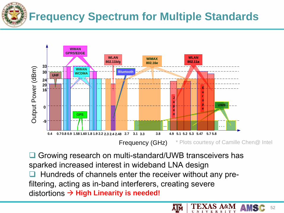
Frequency Spectrum for Multiple Standards
Growing research on multi-standard/UWB transceivers has
sparked increased interest in wideband LNA design
Hundreds of channels enter the receiver without any pre-
filtering, acting as in-band interferers, creating severe
distortions
RF Interference from Frequency Overlap, Out-of-Band Emissions and Receiver Saturation
-9
0
30
20
Output Power (dBm)
24
33
16
3.1 3.3 4.9 5.1 5.2 5.3 5.47 5.7 5.8
Frequency (GHz)
3.8
WiMAX
802.16e
. . .
Y-Axis
...
UWB
0.8 0.9 2.7
GPS
WWAN
WCDMA
1.58 1.60 1.8 1.9 2.2
WLAN
802.11b/g
2.3 2.4 2.48
WWAN
GPRS/EDGE
0.4 0.7
UHF
WLAN
802.11a
Bluetooth
WiMAX
802.16e
WiMAX
802.16e
WLAN
802.11a
E
u
r
o
p
e
J
a
p
a
n
Frequency (GHz)
Ou
tpu
t P
ow
er
(dB
m)
* Plots courtesy of Camille Chen@ Intel
High Linearity is needed!
53
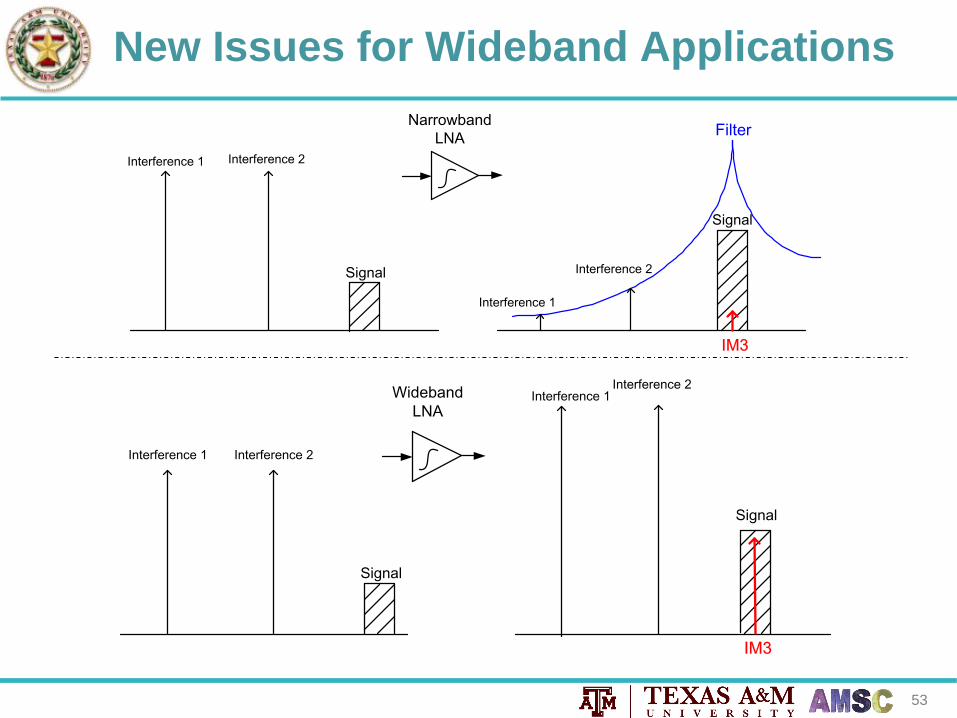
New Issues for Wideband Applications
Interference 1
Signal
Narrowband
LNAFilter
IM3
Interference 2
Interference 1
Interference 2
Signal
Interference 1 Interference 2
Signal
Interference 1Interference 2
Signal
Wideband
LNA
IM3
54
New Issues for Wideband Applications
• Three main concerns:
– IIP2
– P1dB
– IIP2/IIP3 vs. two-tone frequency and spacing
IM3 asymmetry

55
IIP2
• Narrowband system: the 2nd-order nonlinearity
is generally out of band
• Wideband receivers: many channels are
present concurrently and act as in-band
interferences: the IM2 products generated by
certain combination of interferences fall into
the signal band.
• Broadband LNAs should have a good IIP2 as
well as IIP3.
56
IIP2 Improvement Methods
• Fully differential LNA
• Complementary/differential DS method
• Post-distortion
• Biasing a CS-stage at the maximum gain
in deep submicron process
57
1dB Compression Point
• In wideband receivers, LNAs receive the
accumulated power from multiple channels, which
could range from -10 to 0dBm.
• Wideband LNAs are desired to have a high signal-
handling capability, i.e. high P1dB, to prevent
desensitization, gain compression, and clipping.
• IIP2/IIP3-improvement techniques typically only
work over small signal ranges, and do not improve
P1dB because it is a large-signal parameter.

58
P1dB Improvement Methods
• Increasing Vdd above nominal values to maximize the
voltage headroom
• Using low-fT, thick-oxide transistors to handle larger
voltage swings to allow even larger Vdd.
• Cancel higher-order distortion, e.g. IM5 & IM7
• Extend the effective input range of IM2/IM3 cancellation;
• Add source degeneration at the cost of extra noise.
• Dynamic bias/dynamic supply
• Reduce the output voltage swing to relax the limitation
from nonlinear output conductance.

59
IIP2/IIP3 vs. Two-tone Frequency
and Spacing
• Broadband LNAs should have relatively
flat IIP2/IIP3 over the signal band
• IIP2/IIP3 should be examined at various
two-tone-spacing and center frequencies
• Reactive components(e.g. those in the
matching network) causes frequency-
dependence of IIP2/IIP3

60
IIP2/3 dependency on two-tone-spacing
• “2nd-order interaction”
• Large two-tone spacing
• Narrowband IM2 cancellation scheme
• Variations of ∆ω cause the optimum point of the 2nd-order interaction
cancellation to change, resulting in worse linearity.
• “IM3 asymmetry” due to memory effects
Lower IM3 Vector Upper IM3 Vector
H2(2ω1) H
2 (ω2 -ω
1 )
H3(2ω1-ω
2)
H1(ω
1),
H1(-ω
2)
H1(ω
2),
H1(-ω
1)
H3(2ω
2-ω
1)
H2(2ω2)
H2 (ω
2 -ω1 )
Re
Im
Re
Im
61
Outline
• Motivation
• Linearization Techniques
• New Issues for Wideband Applications
• LNA Linearization in Deep Submicron Process
• Remarks for High Linearity LNA Design

62
LNA Linearization in Deep submicron
Technology
• Nonlinearity from output conductance gds
• Impact of Technology Scaling on Linearity

63
Nonlinearity from output conductance gds
• gds nonlinearity becomes more prominent in
scaling down technology
• Current ids is controlled by both Vgs and Vds,
approximated by the two-dimensional Taylor
series:
2 3 2 3
1 2 3 1 2 3
2 2
(1,1) (2,1) (1,2)
,ds gs ds gs gs gs ds ds ds ds ds ds
gs ds gs ds gs ds
i V V g V g V g V g V g V g V
c V V c V V c V V
1
!
i
DSdsi i
DS
Ig
i V
( , )
1
! !
m n
DSm n m n
GS DS
Ic
m n V V

64
gds Nonlinearity Characteristics
• Fix Vgs at 0.5V, sweep the Vds, by taking the first three derivatives of
ids with respect to Vds at every DC bias point, we obtained:
NMOS output conductance nonlinearity characteristics
(UMC 90nm CMOS process, W/L = 20/0.08μm, Vgs = 0.5V, Vth = 0.26V).
gds3 is large when the
transistor operates at
small Vds; it decreases
for large Vds values
gds contributes less
nonlinearity when
device operates
deeper into saturation
region.

65
Impact of Technology Scaling
• gds is more nonlinear for shorter channel length
• Reduced supplydevice biased closer to the triode-saturation
boundary, worsens gds nonlinearity.
• “sweet spot” systematically shift to higher bias-current density
Ids/W requires larger power to preserve linearity.
• Oxide thickness decreases, poly-gate depletion increases,
nonlinear gate capacitance develops strong 2nd-order derivatives
with respect to Vgs significant 3rd-order distortion
• Key challenge: deliver high linearity with core transistors
and with a low supply voltage in the DSM processes.
66
Outline
• Motivation
• Linearization Techniques
• New Issues for Wideband Applications
• LNA Linearization in Deep Submicron Process
• Remarks for High Linearity LNA Design

67
To reduce gds-induced distortion
• Increasing supply voltage mitigates the gds effect, allows
larger output swing and hence improves P1dB.
• with sufficient voltage headroom, adding cascode device
allows gds << RLoad ,yielding a more linear output load.
• bias the cascode transistor at smaller Vgs (i.e. lower
overdrive voltage) to tolerate a larger swing at the drain.
• Reducing the load resistance of the LNA(which may
affect the design of other building blocks in the receiver)

68
Other Tips
• For inductively degenerated CS-LNAs: reduce Q
to mitigate the “Q boosting” effect, provided
enough margin in NF and gain. Add external
capacitor in parallel with Cgs to allow more
freedom for input transistor sizing.
• CG-LNAs generally provide better linearity than
CS-LNAs
• Use cascode transistors whenever possible to:
– reduce 2nd-order interaction through Cgd
– reduce the voltage swing across each active device,
improving reliability for DSM devices.

69
Conclusions
• Reviewed eight categories of CMOS LNA
linearization techniques and discussed the
tradeoffs among linearity, power, and PVT
variations.
• Discussed wideband LNA-linearization issues for
the emerging broadband transceivers
• Examined issues in deep submicron processes
• Presented general design guidelines for high-
linearity LNAs.
70
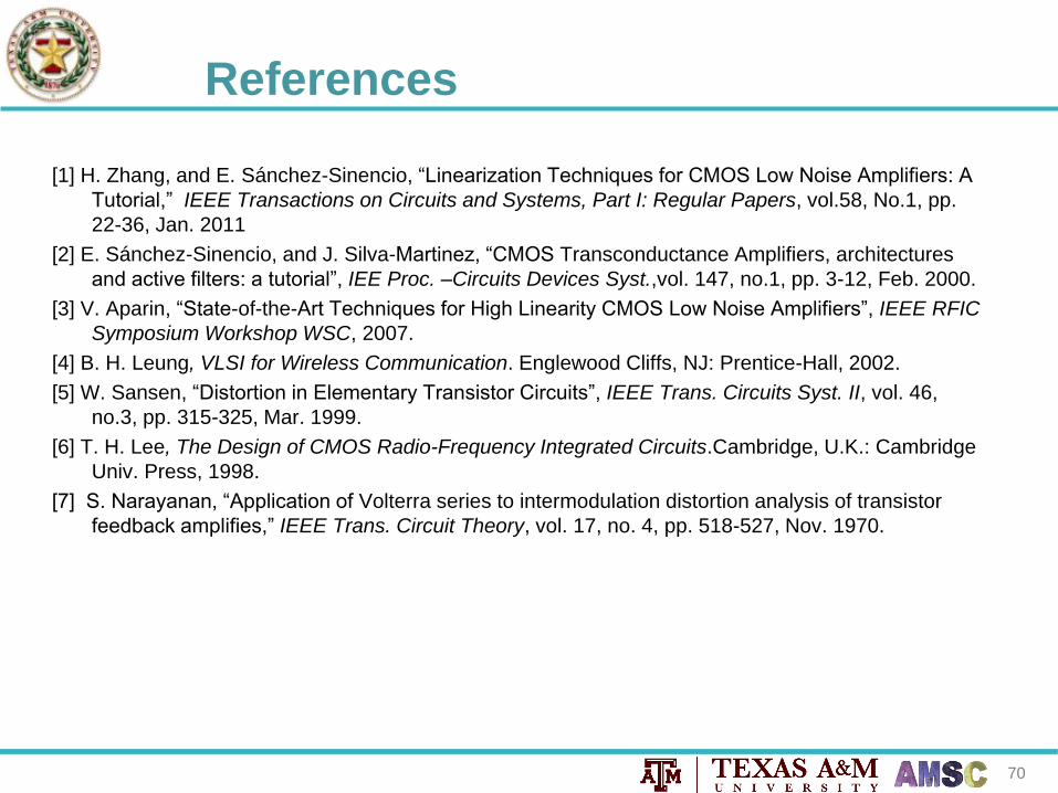
References
[1] H. Zhang, and E. Sánchez-Sinencio, “Linearization Techniques for CMOS Low Noise Amplifiers: A
Tutorial,” IEEE Transactions on Circuits and Systems, Part I: Regular Papers, vol.58, No.1, pp.
22-36, Jan. 2011
[2] E. Sánchez-Sinencio, and J. Silva-Martinez, “CMOS Transconductance Amplifiers, architectures
and active filters: a tutorial”, IEE Proc. –Circuits Devices Syst.,vol. 147, no.1, pp. 3-12, Feb. 2000.
[3] V. Aparin, “State-of-the-Art Techniques for High Linearity CMOS Low Noise Amplifiers”, IEEE RFIC
Symposium Workshop WSC, 2007.
[4] B. H. Leung, VLSI for Wireless Communication. Englewood Cliffs, NJ: Prentice-Hall, 2002.
[5] W. Sansen, “Distortion in Elementary Transistor Circuits”, IEEE Trans. Circuits Syst. II, vol. 46,
no.3, pp. 315-325, Mar. 1999.
[6] T. H. Lee, The Design of CMOS Radio-Frequency Integrated Circuits.Cambridge, U.K.: Cambridge
Univ. Press, 1998.
[7] S. Narayanan, “Application of Volterra series to intermodulation distortion analysis of transistor
feedback amplifies,” IEEE Trans. Circuit Theory, vol. 17, no. 4, pp. 518-527, Nov. 1970.
71
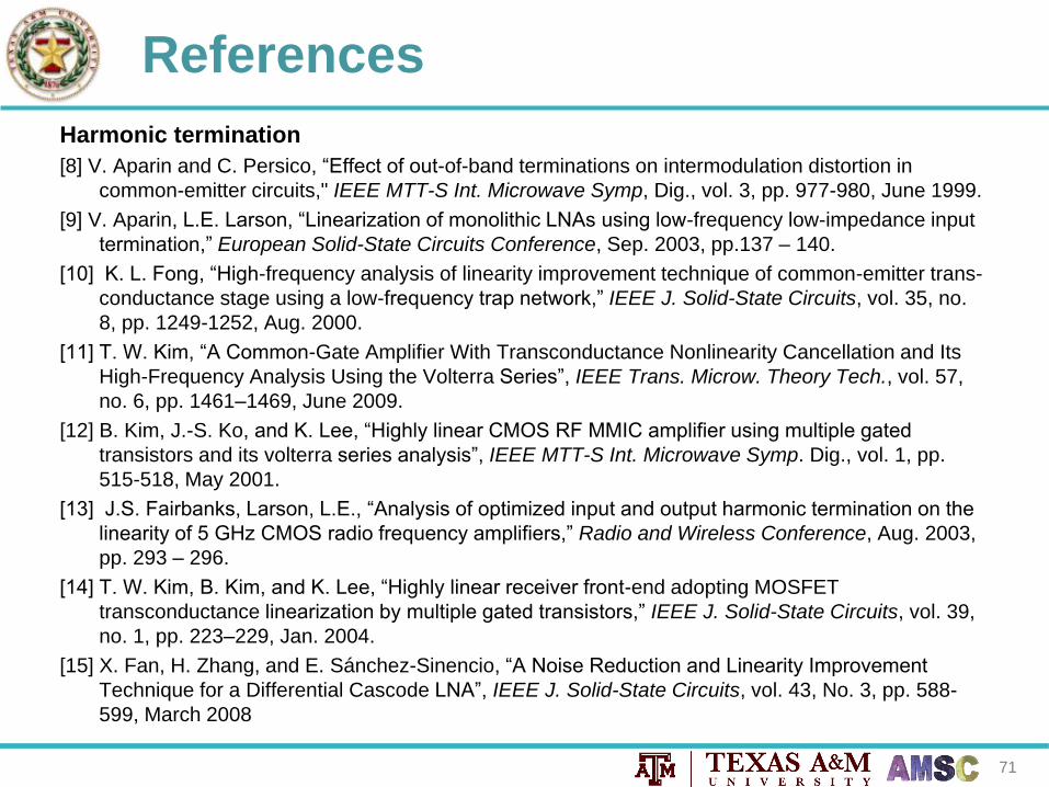
References
Harmonic termination
[8] V. Aparin and C. Persico, “Effect of out-of-band terminations on intermodulation distortion in
common-emitter circuits," IEEE MTT-S Int. Microwave Symp, Dig., vol. 3, pp. 977-980, June 1999.
[9] V. Aparin, L.E. Larson, “Linearization of monolithic LNAs using low-frequency low-impedance input
termination,” European Solid-State Circuits Conference, Sep. 2003, pp.137 – 140.
[10] K. L. Fong, “High-frequency analysis of linearity improvement technique of common-emitter trans-
conductance stage using a low-frequency trap network,” IEEE J. Solid-State Circuits, vol. 35, no.
8, pp. 1249-1252, Aug. 2000.
[11] T. W. Kim, “A Common-Gate Amplifier With Transconductance Nonlinearity Cancellation and Its
High-Frequency Analysis Using the Volterra Series”, IEEE Trans. Microw. Theory Tech., vol. 57,
no. 6, pp. 1461–1469, June 2009.
[12] B. Kim, J.-S. Ko, and K. Lee, “Highly linear CMOS RF MMIC amplifier using multiple gated
transistors and its volterra series analysis”, IEEE MTT-S Int. Microwave Symp. Dig., vol. 1, pp.
515-518, May 2001.
[13] J.S. Fairbanks, Larson, L.E., “Analysis of optimized input and output harmonic termination on the
linearity of 5 GHz CMOS radio frequency amplifiers,” Radio and Wireless Conference, Aug. 2003,
pp. 293 – 296.
[14] T. W. Kim, B. Kim, and K. Lee, “Highly linear receiver front-end adopting MOSFET
transconductance linearization by multiple gated transistors,” IEEE J. Solid-State Circuits, vol. 39,
no. 1, pp. 223–229, Jan. 2004.
[15] X. Fan, H. Zhang, and E. Sánchez-Sinencio, “A Noise Reduction and Linearity Improvement
Technique for a Differential Cascode LNA”, IEEE J. Solid-State Circuits, vol. 43, No. 3, pp. 588-
599, March 2008
72
References Optimum biasing
[16] V. Aparin, G. Brown, and L. E. Larson, “Linearization of CMOS LNAs via optimum gate biasing,”
in IEEE Int. Circuits Syst. Symp., Vancouver, BC, Canada, vol. IV, pp. 748–751, May 2004.
Feedforward
[17] Y. Ding, and R. Harjani, “A +18 dBm IIP3 LNA in 0.35μm CMOS,” in IEEE Int. Solid-State Circuits
Conf. (ISSCC) Dig. Tech. Papers, Feb. 2001, pp. 162–163.
[18] E. Keehr, and A. Hajimiri, “Equalization of IM3 Products in Wideband Direct-Conversion
Receivers,” in IEEE Int. Solid-State Circuits Conf. (ISSCC) Dig. Tech. Papers, Feb. 2008, pp.
204–205.
Derivative Superposition (DS)
[19] Y. S. Youn, J. H. Chang, K. J. Koh, Y. J. Lee, and H. K. Yu, “A 2 GHz 16 dBm IIP3 low noise
amplifier in 0.25 μm CMOS technology,” IEEE Int. Solid-State Circuits Conf. (ISSCC) Dig. Tech.
Papers, Feb. 2003, pp. 452–453.
[20] C. Xin and E. Sánchez-Sinencio, “A linearization technique for RF low noise amplifier,” in IEEE
Int. Circuits Syst. Symp., Vancouver, BC, Canada, vol. IV, pp. 313–316, May 2004.
[21] H.M. Geddada, J.W. Park and J. Silva-Martinez, “Robust derivative superposition method for
linearizing broadband LNAs”, IEE Electronics Letters, vol. 45 no. 9, pp.435-436, April 2009.
[22] T.H. Jin, and T. W. Kim, “A 6.75 mW +12.45 dBm IIP3 1.76 dB NF 0.9 GHz CMOS LNA
Employing Multiple Gated Transistors With Bulk-Bias Control”, IEEE Microw. Wireless Compon.
Lett., vol.21, no.11, pp.616-618, Nov. 2011
73
References
Complementary DS
[23] D. Im, I. Nam, H. Kim, and K. Lee, “A Wideband CMOS Low Noise Amplifier Employing Noise and
IM2 Distortion Cancellation for a Digital TV Tuner”, IEEE J. Solid-State Circuits, vol. 44, No. 3, pp.
686-698, March 2009.
Differential DS
[24] T. W. Kim, and B. Kim, “A 13-dB IIP3 Improved Low-Power CMOS RF Programmable Gain
Amplifier Using Differential Circuit Transconductance Linearization for Various Terrestrial Mobile
D-TV Applications”, IEEE J. Solid-State Circuits, vol. 41, No. 4, pp. 945-953, April 2006.
Modified DS
[25] V. Aparin and L. E. Larson, “Modified derivative superposition method for linearizing FET low-
noise amplifiers,” IEEE Trans. Microw. Theory Tech., vol. 53, no. 2, pp. 571–581, Feb. 2005.
[26] S. Ganesan, E. Sánchez-Sinencio, and J. Silva-Martinez, “A highly linear low noise amplifier”,
IEEE Trans. Microw. Theory Tech., vol. 54, no. 12, pp. 4079-4085, Dec. 2006.
[27] W.Li, J. Tsai, H. Yang, W. Chou, S. Gea, H. Lu, and T. Huang, “Parasitic-Insensitive Linearization
Methods for 60-GHz 90-nm CMOS LNAs” , IEEE Trans. Microw. Theory Tech., vol. 60, no. 8, pp.
2512–2523, Aug. 2012.
IM2 injection
[28] S. Lou and H. C. Luong, “A Linearization Technique for RF Receiver Front-End Using Second-
Order-Intermodulation Injection”, IEEE J. Solid-State Circuits, vol. 43, No. 11, pp. 2404-2412, Nov.
2008.

74
References Noise/Distortion Cancellation
[29] F. Bruccoleri, E. A. M. Klumperink, and B. Nauta, “Wide-band CMOS low-noise amplifier exploiting thermal noise
canceling,” IEEE J. Solid-State Circuits, vol. 39, no. 2, pp. 275–282, Feb. 2004.
[30] J. Jussila, and P. Sivonen, “A 1.2-V Highly Linear Balanced Noise-Cancelling LNA in 0.13-µm CMOS”, IEEE J.
Solid-State Circuits, vol. 43, No. 3, pp. 579-587, Mar. 2008.
[31] W.Chen, G.Liu, B.Zdravko, and A.M. Niknejad, “A Highly Linear Broadband CMOS LNA Employing Noise and
Distortion Cancellation”, IEEE J. Solid-State Circuits, vol. 43, No. 5, pp. 1164-1176, May 2008.
[32] S. C. Blaakmeer, E. A. M. Klumperink, D. M. W. Leenaerts, and B. Nauta, “Wideband Balun-LNA with
Simultaneous Output Balancing, Noise-Canceling and Distortion-Canceling”, IEEE J. Solid-State Circuits, vol. 43,
No. 6, pp. 1341-1350, June 2008.
[33] W. Cheng, A. Annema, G.J.M. Wienk, and B. Nauta, “A Wideband IM3 Cancellation Technique using Negative
Impedance for LNAs with Cascode Topology”, in IEEE RFIC Symp. Dig., Montreal, Canada, 2012, pp. 13–16.
Post-distortion
[34] N. Kim, V. Aparin, K. Barnett, and C. Persico, “A cellular-band CDMA CMOS LNA linearized using active post-
distortion,” IEEE J. Solid-State Circuits, vol. 41, no. 7, pp. 1530–1534, Jul. 2006.
[35] T.-S. Kim and B.-S. Kim, “Post-linearization of cascode CMOS LNA using folded PMOS IMD sinker,” IEEE Microw.
Wireless Comp. Lett., vol. 16, no. 4, pp. 182–184, Apr. 2006.
[36] H. Zhang, X. Fan, and E. Sánchez-Sinencio, “A low-power, linearized, ultra-wideband LNA design technique,”
IEEE J. Solid-State Circuits, vol. 44, no. 2, pp. 320–330, Feb. 2009.
[37] W.Li, J. Tsai, H. Yang, W. Chou, S. Gea, H. Lu, and T. Huang, “Parasitic-Insensitive Linearization Methods for 60-
GHz 90-nm CMOS LNAs” , IEEE Trans. Microw. Theory Tech., vol. 60, no. 8, pp. 2512–2523, Aug. 2012. (*
appear in both the DS method and post-distortion category because it talks about both methods)
75
References
IIP2 calibration
[38] D. Kaczman, M. Shah, M. Alam, M. Rachedine, D. Cashen, L. Han, and A. Raghavan, “A Single-
Chip 10-Band WCDMA/HSDPA 4-Band GSM/EDGE SAW-less CMOS Receiver With DigRF 3G
Interface and +90 dBm IIP2,” IEEE J. Solid-State Circuits, vol. 44, no. 3, pp. 718-739, March 2009.
[39] M. Hotti, J. Ryynanen, K. Kivekas, and K. Halonen, “An IIP2 Calibration Technique for Direct
Conversion Receivers”, in IEEE Int. Circuits Syst. Symp., Vancouver, BC, Canada, vol. IV, pp. 257–
260, May 2004.
[40] W. Kim, S. Yang, Y. Moon, J. Yu, H. Shin, W. Choo, and B. Park, “IP2 calibrator Using Common
Mode Feedback Circuitry”, European Solid-State Circuits Conference, 2005, pp.231 – 234.
[41] H. Darabi, H. Kim, J. Chiu, B. Ibrahim, and L. Serrano, “An IP2 Improvement Technique for Zero-IF
Down-Converters”, in IEEE Int. Solid-State Circuits Conf. (ISSCC) Dig. Tech. Papers, Feb. 2006.
IIP2/IIP3 dependence on two tone spacing
[42] W. Bosch and G. Gatti, “Measurement and simulation of memory effects in predistortion
linearizers,” IEEE Trans. Microwave Theory Tech., vol. 37, pp. 1885–1890, Dec. 1989.
[43] J. F. Sevic, K. L. Burguer, and M. B. Steer, “A novel envelope-termination load–pull methods for
ACPR optimization of RF/microwave power amplifiers,” in IEEE MTT-S Int. Microwave Symp. Dig.,
Baltimore, MD, 1998, pp. 601–605.
[44] N. Borges de Carvalho and J. C. Pedro, “Two-tone IMD asymmetry in microwave power amplifiers,”
in IEEE MTT-S Int. Microwave Symp. Dig., Boston, MA, 2000, pp. 445–448.
[45] N. Carvalho, and J. Pedro, “A Comprehensive Explanation of Distortion Sideband Asymmetries”,
IEEE Trans. Microw. Theory Tech., vol. 50, no. 9, pp. 2090-2101, Sep. 2002.

76
References
Others
[46] N. Cowley, and R. Hanrahan. (2005, Nov. 10). ATSC compliance and tuner design implications.
Video/Imaging Design Line [Online]. Available:
http://www.videsignline.com/showArticle.jhtml?articleID=173601582
[47] S. S. Taylor, and J. S. Duster, “High-linearity low noise amplifier and method,” U. S. Patent 0 278
220, Nov. 13, 2008.
LNA linearization in deep submicron technology
[48] S. Kang, B. Choi, and B. Kim, “Linearity Analysis of CMOS for RF Application,” IEEE Trans.
Microw. Theory Tech., vol. 51, no. 3, pp. 972-977, Mar. 2003.
[49] B. Toole, C. Plett, and M. Cloutier, “RF Circuit Implications of Moderate Inversion Enhanced
Linear Region in MOSFETs,” IEEE Trans. Circuits Syst. I, Reg. Papers, vol. 51, no. 2, pp. 319–
328, Feb. 2[45] R. A. Baki, T. K. K. Tsang, and M. N. El-Gamal, “Distortion in RF CMOS Short-
Channel Low-Noise Amplifiers,” IEEE Trans. Microw. Theory Tech., vol. 54, no. 1, pp. 46-56, Jan.
2006.
[50] C. H. Choi, Z. Yu, and R. W. Dutton, “Impact of poly-gate depletion on MOS RF linearity,” IEEE
Electron Device Lett., vol. 24, no. 5, pp. 330–332, May 2003.
[51] R. van Langevelde, L. F. Tiemeijer, R. J. Havens, M. J. Knitel, R. F. M. Ores, P. H.Woerlee, and
D. B. M. Klaassen, “RF-distortion in deepsubmicron CMOS technologies,” in IEEE IEDM Tech.
Dig., pp.807–810, 2000.
[52] T. Lee, and Y. Cheng, “High-Frequency Characterization and Modeling of Distortion Behavior of
MOSFETs for RF IC Design”, IEEE J. Solid-State Circuits, vol. 39, no.9, pp. 1407-1414, Sep.
2004.


