Active-matrix liquid-crystal-display ~LCD! projec-tion systems have been available for years. Be-cause of their relatively low cost, compact size, lightweight, high resolution, and compatibility withcomputers and various multimedia equipment,their market share is growing rapidly.1 In manyapplications, these systems have replaced CRT-based or light-valve-based projection systems.However, one disadvantage of the LCD projectionsystems is the pixel structure shown on the projec-tion screen. In an active-matrix LCD panel, athin-film transistor is deposited in each pixel andelectric connections are led to all transistors. Theareas corresponding to these transistors and elec-tric connections are opaque and are known as adead space or a dead zone. The fill factor is definedas the ratio between the active area ~where thetransmitting optical intensity is modulated! andthe nominal pixel size ~determined by the center-
X. Yang and N. Li are with the Department of Electrical Engi-neering, University of New Orleans, New Orleans, Louisiana70148; S. Jutamulia is with Photonics Research, Inc., 38730 Lex-ington Street, Fremont, California 94536.Received 17 January 1996; revised manuscript received 15 April
to-center distance of pixels!. Typically, the fill fac-tor of a LCD panel is between 45% and 65%.When the LCD is projected onto the screen, the
dead spaces generate a two-dimensional ~2-D! darkscreen over the projected image that causes an un-comfortable scene to viewers. Several techniqueshave been proposed to remove the pixel structurefrom the projected images,2–6 and a review of thesetechniques can be found in Ref. 2. In this Note wepresent, to our knowledge, the first experimentaldemonstration of a phase-scrambling method for theremoval of LCD pixel structures. This method re-quires only a transparent mask with different thick-nesses at the locations corresponding to the variousdiffraction orders. The difference in thickness be-tween any pair of subareas causes an optical pathdifference longer than the coherence length of thelight source. Because the white light sources usedin most of LCD’s cover the whole visible range, theyhave a very short coherence length, usually less thana micrometer. After passing through such a trans-parent mask, the phase among different spatial spec-tra is scrambled, and the images originating fromeach of them superimpose incoherently on the projec-tion screen. The dark lines of the dead zone, whichis the result of the interference of all spatial spectralcomponents, disappear, and the projected image re-mains sharp and focused. The principle of this ap-proach and preliminary experimental results arepresented in the following sections.
10 August 1996 y Vol. 35, No. 23 y APPLIED OPTICS 4577
2. Depixelization by Use of a Phase-Scrambling Filter
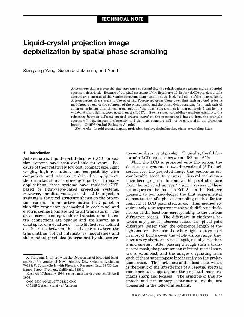
The pixel structure of a LCD panel generates multi-ple Fourier spectra. Each single spectrum containsall the information to form the image. When theimages originating from different spatial spectra su-perimpose at the projection-image plane, however,the phase relation among these spectra produces theinterference that is the image of dead zones. If thephase relation between these spectra is scrambled,the images will be incoherently superimposed, andthe dead-zone image can be removed.Figure 1 schematically illustrates an LCD projec-
tion system. Light from the light source S is pro-jected ~preferably collimated! by lens L1 to the LCDpanel. Mirror M reflects a portion of the optical en-ergy back to the aperture of L1 to improve the lightefficiency. An input scene is fed into the LCD panel,which is imaged onto the projection screen by theimaging lens L2.LCD’s are two dimensional in nature; however, for
simplicity and yet without a loss of generality, thediscussion in this section is limited to the 1-D case.The transmission function of a LCD panel with 2M 11 pixels can be characterized as
t~x! 5 (m52M
M
rectSx 2 mDxX D , (1)
where rect~. . .! denotes the rectangle function, Dx isthe center-to-center distance of pixels, and X is thewidth of the pixel active area. An input signal dis-played in such a LCD, s~x!, is sampled by LCD pixels.To abbreviate the tedious mathematical representa-tion and yet model the sampling nature of each pixel,we can model the transmission function with a sim-plified representation as
t~x! 5 (m52`
`
d~x 2 mDx!. (2)
To represent the LCD with Eq. ~2!, we have assumeda large number of pixels, a uniform pixel structure,and slow variance of the input signal over the LCDpanel, which properties are generally true in practice.Assume that the LCD is illuminated by a colli-
mated white light beam, then the optical field behind
Fig. 1. Schematic diagram of a LCD projection system.
4578 APPLIED OPTICS y Vol. 35, No. 23 y 10 August 1996
the LCD panel can be written as
l~x! 5 s~x!t~x! 5 s~x! (m52`
`
d~x 2 mDx!. (3)
The Fourier spectrum is obtained at the back focalplane of the image lens as7
L~m, l! 5 S~m, l! ^ (n52`
`
d~m 2 mDm, l!
5 (m52`
`
S~m 2 mDm, l!, (4)
where S~m, l! is the Fourier transform of the inputsignal, the cross within the circle denotes the convo-lution operator, and Dm 5 1yDx is the distance be-tween adjacent spectral orders, which is determinedby the pixel pitch of the LCD. It should be notedthat the Fourier spectrum is wavelength dependent:The shorter the wavelength, the closer the spectrumis to the center of the spectral plane. As the opticalwave propagates from the back focal plane to theimage plane, the inverse Fourier transform is accom-plished naturally,7 and the amplitude of the image isgiven by
l~x! 5 s~x! (m52`
`
d~x 2 mDx!, (5)
which is identical to Eq. ~3!, and the pixel structure,represented by • d~x 2 mDx!, is preserved.For removing the pixel structure, a transparent,
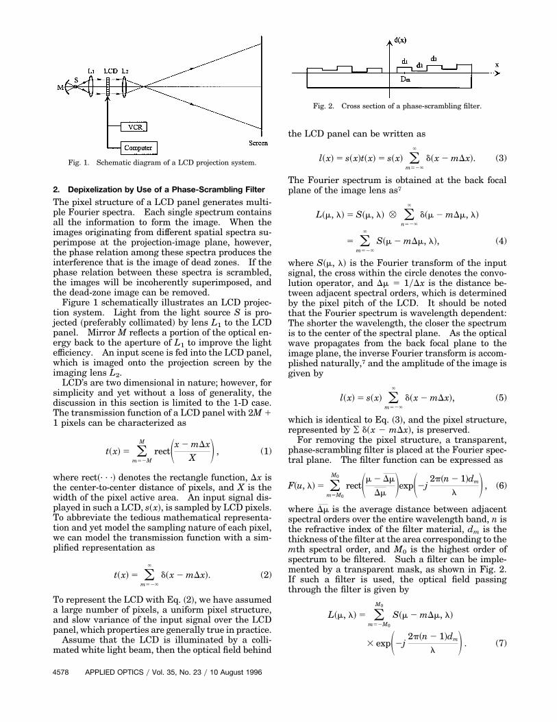
phase-scrambling filter is placed at the Fourier spec-tral plane. The filter function can be expressed as
F~u, l! 5 (m5M0
M0
rectSm 2 Dm
Dm DexpS2j 2p~n2 1!dml D , (6)
where Dm is the average distance between adjacentspectral orders over the entire wavelength band, n isthe refractive index of the filter material, dm is thethickness of the filter at the area corresponding to themth spectral order, and M0 is the highest order ofspectrum to be filtered. Such a filter can be imple-mented by a transparent mask, as shown in Fig. 2.If such a filter is used, the optical field passingthrough the filter is given by
L~m, l! 5 (m52M0
M0
S~m 2 mDm, l!
3 expS2j2p~n 2 1!dm
l D . (7)
Fig. 2. Cross section of a phase-scrambling filter.
Again, the inverse Fourier transform is obtained atthe image plane, which can be written as
L~x! 5 (m52M0
M0
s~x!expS2j2pxDx D
3 expF2j2p~n 2 1!dm
l G . (8)
The third term is caused by the filter. It disturbs thephase relation between the images originating fromdifferent spectral orders such that the interferencebetween these images does not clearly generate theregular pixel structure ~i.e., image of the dead zones!.In particular, if the optical path difference betweeneach pair of subareas in the phase mask is longerthan the coherent length of the light source, the re-constructed images from multiple spectra will super-impose incoherently. Then the intensity of thesuperimposed image is given by
O~x! 5 (m52M0
M0 Us~x!expS2j 2pxDx DexpF2j 2p~n2 1!dm
l GU25 ~2M0 1 1!us~x!u2. (9)
A sharp, continuous-tone image is observed, with thepixel structure removed.It should be noted that the finite aperture of the
LCD panel is not considered in the above discussion@that following Eq. ~2!#. The finite aperture causesthe limited number of diffraction orders. In prac-tice, the three or five lowest diffraction orders ~i.e.,the 0, 61, and 62 orders! contain most of lightenergy. Therefore only a limited number of subar-eas is required for a phase-scrambling filter. Therest of the areas corresponding to higher diffractionorders can be either opaque, with a modest loss inlight efficiency, or transparent, with a slightly re-duced depixelization effect. The difference in thethickness of the filter subarea is required by
di 2 dj . Ddmin 5Dl
~n 2 1!, i Þ j, (10)
where Dl 5 l2yDl is the coherence length of the lightsource. For most of the white light sources coveringthe whole visible and near-infrared range, the coher-ence length is approximately 0.5 mm and Ddmin is ofthe order of 1mm. In color LCD projectors, the whitelight passes through dichroic mirrors and illuminatesthree LCD panels, corresponding to components R, G,and B ~red, green, and blue, respectively!. If thewavelength bandwidth of each color is approximately0.1 mm, the corresponding coherence length is be-tween 2 and 3.5 mm, which requires a Ddmin rangingfrom 4 to 7 mm. Filters with such specifications canreadily be fabricated with various techniques, such asdry etching or lithography.
3. Experimental Demonstration
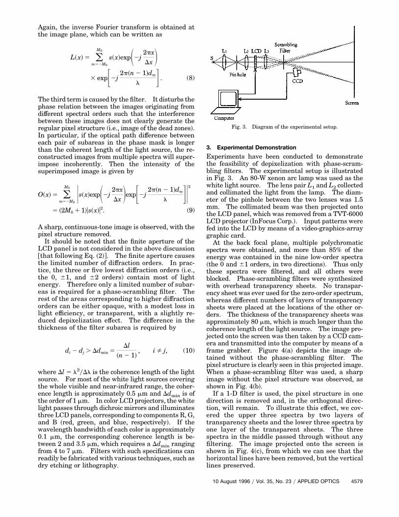
Experiments have been conducted to demonstratethe feasibility of depixelization with phase-scram-bling filters. The experimental setup is illustratedin Fig. 3. An 80-W xenon arc lamp was used as thewhite light source. The lens pair L1 and L2 collectedand collimated the light from the lamp. The diam-eter of the pinhole between the two lenses was 1.5mm. The collimated beam was then projected ontothe LCD panel, which was removed from a TVT-6000LCD projector ~InFocus Corp.!. Input patterns werefed into the LCD by means of a video-graphics-arraygraphic card.At the back focal plane, multiple polychromatic
spectra were obtained, and more than 85% of theenergy was contained in the nine low-order spectra~the 0 and 61 orders, in two directions!. Thus onlythese spectra were filtered, and all others wereblocked. Phase-scrambling filters were synthesizedwith overhead transparency sheets. No transpar-ency sheet was ever used for the zero-order spectrum,whereas different numbers of layers of transparencysheets were placed at the locations of the other or-ders. The thickness of the transparency sheets wasapproximately 80 mm, which is much longer than thecoherence length of the light source. The image pro-jected onto the screen was then taken by a CCD cam-era and transmitted into the computer by means of aframe grabber. Figure 4~a! depicts the image ob-tained without the phase-scrambling filter. Thepixel structure is clearly seen in this projected image.When a phase-scrambling filter was used, a sharpimage without the pixel structure was observed, asshown in Fig. 4~b!.If a 1-D filter is used, the pixel structure in one
direction is removed and, in the orthogonal direc-tion, will remain. To illustrate this effect, we cov-ered the upper three spectra by two layers oftransparency sheets and the lower three spectra byone layer of the transparent sheets. The threespectra in the middle passed through without anyfiltering. The image projected onto the screen isshown in Fig. 4~c!, from which we can see that thehorizontal lines have been removed, but the verticallines preserved.
Fig. 3. Diagram of the experimental setup.
10 August 1996 y Vol. 35, No. 23 y APPLIED OPTICS 4579
Fig. 4. Experimental results: ~a! image obtained without filter-ing, ~b! image obtained with 2-D filtering, and ~c! image obtainedwith 1-D filtering.
4580 APPLIED OPTICS y Vol. 35, No. 23 y 10 August 1996
4. Conclusions
The pixel structure in LCD’s causes an uncomfort-able scene to viewers. The pixel structure can beremoved by random scrambling of the relativephase among the multiple spatial spectra. Aphase-scrambling filter is virtually a transparentmask with different thicknesses at subareas corre-sponding to the multiple Fourier spectral orders.Because most of the light energy is contained in afew low-order spectra, only a limited number ofthickness values are needed. Such a filter has theadvantages of robustness, a small size, a low cost,and a light weight. It can easily be integrated intocurrent LCD projection systems. The feasibilityand effectiveness of a phase-scrambling filter havebeen experimentally demonstrated. The integra-tion of this technique into current LCD systems ispresently under investigation.
References1. J. C. Fan, “Flat-panel displays: the next technology gold rush,”
Photon. Spectra January 122–123 ~1995!.2. S. Jutamulia, S. Toyota, and Y. Ichihashi, “Removal of pixel
structure in liquid crystal projection display,” Proc. SPIE 2407,168–176 ~1994!.
3. S. Kelly, “Removing the pixel structure from projected imagesusing a transparent filter,” Proc. SPIE 1664, 153–159 ~1992!.
4. E. Dolgoff, “New optical designs for large screen, 2- and 3-di-mensional video projection with enhanced brightness and novisible pixel or line structure,” Proc. SPIE 2407, 104–118~1994!.
5. H.-K. Liu, “Large area projection liquid-crystal video displaysystem with inherent grid pattern optically removed,” U.S.patent 5,161,027 ~NASA Jet Propulsion Laboratory, 4800 OakGrove Drive, Pasadena, Calif. 91109, 1992!.
6. E. N. Hogert and N. Gaggioli, “Incoherent 2-D spatial filteringof screen images,” Appl. Opt. 29, 2564–2568 ~1990!.
7. J. W. Goodman, Introduction to Fourier Optics ~McGraw-Hill,New York, 1968!.