Liquid-crystal-tunable metal–insulator–metal plasmonic waveguides and Bragg resonators This article has been downloaded from IOPscience. Please scroll down to see the full text article. 2013 J. Opt. 15 055009 (http://iopscience.iop.org/2040-8986/15/5/055009) Download details: IP Address: 138.73.1.36 The article was downloaded on 03/09/2013 at 07:30 Please note that terms and conditions apply. View the table of contents for this issue, or go to the journal homepage for more Home Search Collections Journals About Contact us My IOPscience
Transcript
Liquid-crystal-tunable metal–insulator–metal plasmonic waveguides and Bragg resonators
This article has been downloaded from IOPscience. Please scroll down to see the full text article.
2013 J. Opt. 15 055009
(http://iopscience.iop.org/2040-8986/15/5/055009)
Download details:
IP Address: 138.73.1.36
The article was downloaded on 03/09/2013 at 07:30
Please note that terms and conditions apply.
View the table of contents for this issue, or go to the journal homepage for more
Home Search Collections Journals About Contact us My IOPscience
Received 24 January 2013, accepted for publication 20 March 2013Published 11 April 2013Online at stacks.iop.org/JOpt/15/055009
AbstractThe dispersive properties of liquid-crystal-tunable metal–insulator–metal plasmonicwaveguides are theoretically investigated as a function of the applied control voltage. The LCreorientation study is rigorously coupled to the optical studies via a multiphysicsfinite-element analysis. A Bragg grating resonator is designed based on the proposedwaveguide, which shows an extensive tuning efficiency of more than 100 nm V−1 for lowoperating voltages up to 2 V.
(Some figures may appear in colour only in the online journal)
1. Introduction
The scientific field of plasmonics, which deals with theproperties of surface localized or propagating optical fieldsat metal/dielectric interfaces, has lately been attracting arapidly growing research interest that spans over a broadrange of disciplines and paves the way for unprecedentedapplications [1]. Among these, plasmonics are envisaged asa platform for future integrated photonic architectures, owingto their unique capability of providing sub-wavelength lightconfinement [2–5]. One of the most widely explored designapproaches towards nanoscale plasmonic integrated circuitryis based on the metal–insulator–metal (MIM) waveguide,which is formed by a dielectric sandwiched between twometal slabs, typically silver or gold [6, 7]. Starting from thegeneric MIM structure, a series of key components in photoniccircuitry have been demonstrated, such as stub-filters [8],linear [9] or non-linear [10] resonators, as well as Braggwaveguide filters and resonators [11–14].
Apart from passive components, such as filters, powersplitters or junctions, the functionalities required for reallight routing and switching applications also demand circuit
elements that can be externally tuned via a controlmechanism, such as the thermo-, electro-optic or non-lineareffects. Among these possibilities, a family of tunablephotonic devices has thus far been based on the use of nematicliquid crystals (LC), inherently anisotropic materials, whoseproperties can be controlled by applying an electric field [15].Their high optical anisotropy and their extremely low powerconsumption have favored their use in numerous photonicplatforms [16], such as tunable resonators [17], gratings [18,19], photonic crystals [20–22], or phase-shifters [23], whilethey are also currently being explored as an efficient meansof controlling nanoplasmonic resonant structures [24]. In thecontext of guided-wave plasmonics, LC-tunable waveguidesof various designs have been proposed as the core elementof low-power variable attenuators [25], phase-shifters [26],switches [27, 28], filters [29], tunable lenses [30], beamsteerers [31, 32], or modulators [33, 34].
In this work we investigate the dispersive properties ofmetal–liquid-crystal–metal (MLCM) waveguides and reportthe design of a novel LC-tunable Bragg grating filterand resonator, based on experimentally demonstrated MIMstructures [14]. In contrast to previous designs of MLCM
J. Opt. 15 (2013) 055009 D C Zografopoulos and R Beccherelli
plasmonic components [29, 31, 32], the LC orientationproblem is rigorously studied by solving for the underlyingmultiphysics elastic/electrostatic problem for realistic LC-driving conditions. We demonstrate that, by infiltrating a100 nm gold MIM waveguide with the common nematicmaterial E7, the Bragg resonant wavelength can be efficientlytuned over 100 nm by varying the applied control voltagebetween 1 and 2 V, by exploiting the large LC electro-opticeffect. Such tunable plasmonic components may be usedin ultra-low-consumption, highly tunable components insub-wavelength integrated photonic circuitry.
2. Metal–liquid-crystal–metal waveguides
The proposed plasmonic/liquid-crystal waveguide is derivedfrom the MIM template by substituting the isotropic insulatormaterial with a nematic liquid crystal, as shown in the layoutfigure 1(a). The well-known commercial nematic mixture E7is infiltrated between two gold slabs separated by a distanced = 100 nm. Such a configuration allows for the efficientapplication of the control voltage VLC across the nematicLC layer. The LC local molecular orientation is, in general,described by the director, a unit vector that can be defined viatwo angles, tilt and twist, as in figure 1(b). Layers of rubbedpolyimide are most commonly used to promote alignmentof the director in LC devices. However, photo-alignmenttechniques [35] are less harmful to soft thin gold layers andsuitable for photonic applications [36]. They are also effectiveeven when as thin as 3 nm, thus negligibly impacting theoptical properties [37].
In a first approximation, where the LC is in-plane oriented(φ = π/2) along a fixed direction given by a constant angleθ , the dispersive properties of the MLCM waveguide can beanalytically calculated [38, 39]. Such structures have beenproposed as the elements of liquid-crystal based plasmonicbeam steerers [31, 32]. Under more realistic conditions, theLC angles are spatially dependent and may be calculatedby solving the coupled elastic/electrostatic multiphysicsproblem, which minimizes the total energy stored in the LCbulk [40, 26]. In the MLCM waveguide under study, forstrong homogeneous [41] anchoring along the z-axis for theLC molecules at the Au/LC interfaces, the nematic directoris a function of the tilt angle θ(y) only and can be calculatedby solving the set of non-linear equations, which describe aFreedericksz transition problem,
(K11 cos2θ + K33 sin2θ)θ + ((K33 − K11)θ2
+ ε01εV2) sin(θ) cos(θ) = 0 (1)
1ε sin(2θ)θ V + (εo +1ε sin2θ)V = 0, (2)
where single and double dots denote first and secondderivatives over y, respectively. The constants Kii refer tothe LC elastic constants, while εo and εe are the LCordinary and extraordinary low-frequency relative dielectricpermittivities, respectively, with 1ε = εe − εo. The selectednematic material (E7) is characterized by εo = 5.3, εe = 18.6and elastic constants K11 = 10.3 pN,K22 = 7.4 pN,K33 =
16.48 pN [42].
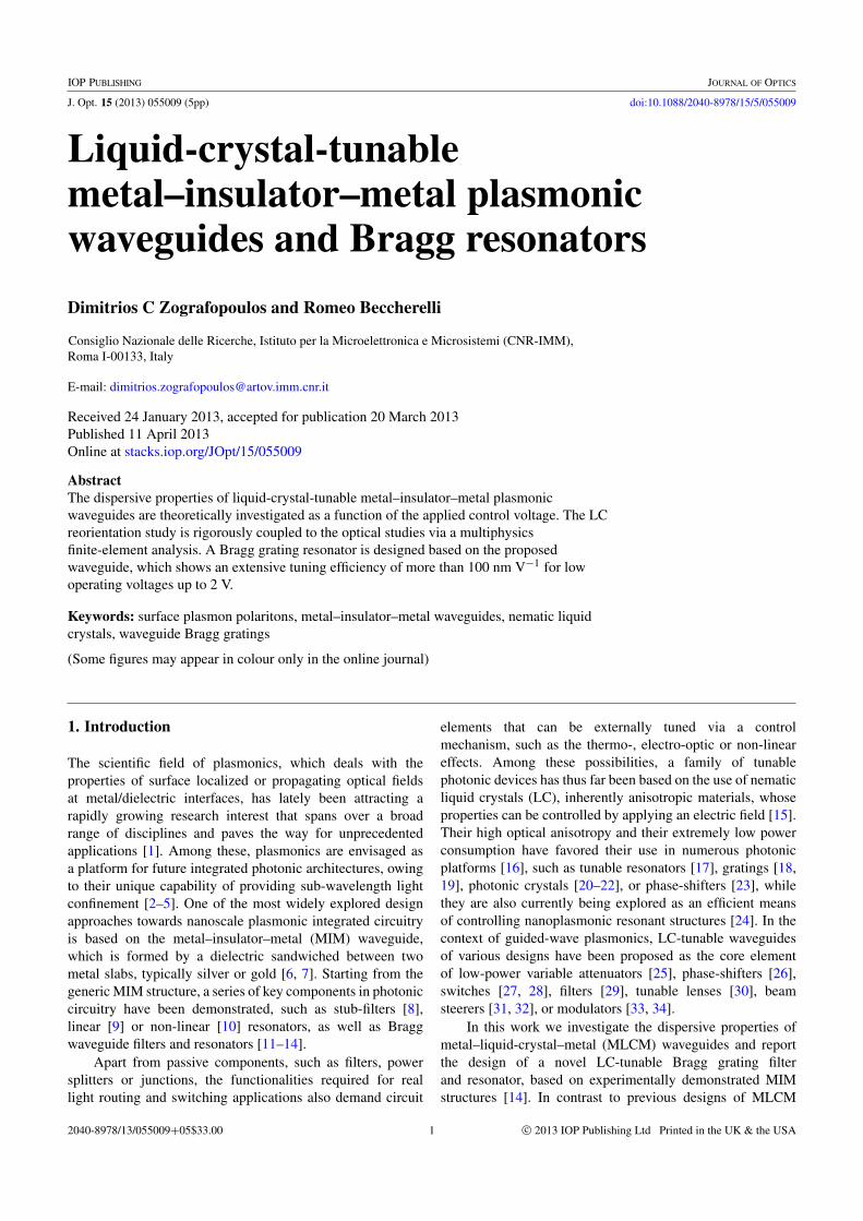
Figure 1. (a) Schematic layout of the MLCM waveguide understudy. The spacing between two infinite gold slabs is infiltrated witha nematic LC. A voltage is applied between the two slabs, whichreorientates the LC molecules. (b) Definition of the tilt and twistangles that describe the nematic director. The SPP mode propagatesalong the x-axis. (c) Tilt angle profile across a 100 nmgold–LC–gold waveguide, infiltrated with the nematic mixture E7,with respect to the applied voltage VLC. Results shown for voltagesranging from 1 to 5 V, in steps of 0.25 V.
Figure 1(c) shows the tilt angle profiles across the LClayer as a function of the applied voltage. The thresholdvoltage for the Freedericksz transition was found equal toVc = 0.93 V. As the applied voltage takes higher values,further tilting close to the LC/Au interfaces is inhibited bythe anchoring boundary conditions. The tilting of the LCmolecules directly influences the dispersive properties, i.e.,the effective index of the plasmonic waveguide mode. Sincethe latter is TM-polarized [7], light primarily senses the nyycomponent of the optical refractive index tensor, which is
given by nyy =
√n2
o + (n2e − n2
o)sin2θ , where no and ne arethe LC ordinary and extraordinary indices, respectively. Thus,increased tilt angle values lead to higher effective indices ofthe fundamental MLCM mode. The modal dispersion curveswith respect to the applied voltage are shown in figure 2.All calculations have been performed via a fully anisotropicfrequency-domain finite-element method [43], by using thetilt and twist angle profiles, as these were derived by the LCswitching studies, for the definition of the optical anisotropytensor. Material dispersion is provided via the Cauchy modelfor E7 [44] and the Drude-critical points model for Au [45].
In order to facilitate comparison, we have includedtwo limit cases, i.e., for an application of zero and infinitevoltage values, which correspond to perfect alignment of
2
J. Opt. 15 (2013) 055009 D C Zografopoulos and R Beccherelli
Figure 2. Effective index of the fundamental TM-polarizedplasmonic mode supported by the MLCM waveguide under study asa function of the applied voltage. Zero and infinite voltage valuescorrespond to perfect alignment of the LC molecules along the z-and y-axis, respectively.
the LC molecules along the z- and y-axis, respectively.Consistent with the tilt profiles calculated in figure 1(c),it can be observed that the tuning of the dispersion curvebecomes progressively hindered for higher voltage values,owing to the anchoring conditions. In particular, these definethe effective index sensed by TM-polarized light near theAu/LC interfaces, where it is known that the optical fieldobtains its maximum values [7]. Nevertheless, results clearlydemonstrate that extensive tuning is possible within smallintervals of applied voltage values.
3. Metal–liquid-crystal–metal Bragg resonators
In this section we present a liquid-crystal-tunable plasmonicresonator based on the MLCM Bragg grating designshown in figure 3(a). This design is compatible withrecently reported experimental studies of MIM Bragg gratingwaveguides fabricated by electron beam lithography/dryetching techniques [14]. The corrugation of the upper goldslab forms a Bragg grating with period d = 2d1 = 2d2 =
380 nm, which is interrupted by a defect cavity of lengthdc = d. The waveguide’s width is w = 100 nm and theetching depth is ed. The filter’s response as a function ofthe etching depth is studied in figure 3(b), for VLC = 0. Asexpected, lower values of ed lead to smoother modulationand a more flattened response of the transmission spectrum.Furthermore, for higher values of ed a red-shift of the bandgapand resonances is observed, as the effective modal index israised in the regions with waveguide width equal to g, whichin turns leads to higher Bragg wavelengths [14]. In addition,deeper etching also enhances the reflectivity of the Braggmirrors, resulting in higher quality factors for the cavity, albeitat the expense of reduced transmission.
The voltage-tunable response of the structure isinvestigated in the results shown in figure 4 for an etchingdepth ed = 30 nm. Results can be directly juxtaposed with
Figure 3. (a) Schematic layout of the proposed MLCM Bragggrating resonator with the definition of material and structuralparameters. (b) Transmission of the MLCM Bragg grating resonatorfor VLC = 0 as a function of the etching depth ed = w− g. Otherparameters: d1 = d2 = 190 nm, dc = 380 nm, and L = 3.8 µm.
Figure 4. Transmission of the MLCM Bragg grating resonator offigure 3 for ed = 30 nm as a function of the applied voltage VLC.
those of figure 2 in order to elucidate the impact of tuningthe modal effective index of the basic MLCM waveguideon the properties of the resonating Bragg grating understudy. The application of the control voltage increases therefractive index sensed by TM-polarized light, leading toa red-shift of the bandgap and the resonating wavelength.The reference cases, namely zero and infinite voltage value,show the ultimate tuning limits of the structure. In-between,the LC is partially switched, as demonstrated in figure 5,which shows the spatial distributions of the electrostaticpotential and the tilt and twist angles for an applied voltageof 1.5 V zoomed in the region around the defect cavity. The
3
J. Opt. 15 (2013) 055009 D C Zografopoulos and R Beccherelli
Figure 5. Electrostatic potential, tilt, and twist angle distribution inthe region around the defect cavity for an applied voltageVLC = 1.5 V.
corrugation creates a slight modulation of the potential and tiltangles, while twist angle lobes are formed around the edges ofthe grating’s teeth, owing to the non-negligible x-componentof the electrostatic field at those regions. However, in terms ofthe structure’s optical properties the twist angle does not havea major impact, since the SPP propagating mode is purelyTM-polarized.
Results indicate that an application of a voltage of up to5 V is sufficient to cover almost the entire available tuningrange. Apart from the anchoring conditions, the achievabletuning range is also limited by dielectric breakdown of theLC material at a certain high voltage threshold. According toexperimentally measured values for nematic materials [46],the maximum applied VLC in the structure under study canbe approximated at ∼2.5 V, taking into account the closestdistance between the two gold electrodes, namely g = 70 nm.Nevertheless, in an experimentally demonstrated LC-tunablesilicon phase shifter [23], a voltage of 5 V was applied overa nematic LC infiltrated in a 100 nm slot, showing thatcontrolling LCs in such confined geometries can be efficientin practice.
Figure 6 compares the electric field profile calculated atλ0 = 1534 nm, which is the Bragg resonant wavelength foran applied voltage of 1.5 V, with two off-resonant cases forVLC = 0 and 3 V. As expected, the electric field is maximizedin the cavity region at the resonant wavelength. The zoomedregions show the SPP modal profile in the absence of anapplied voltage and for VLC = 3 V. When a voltage abovetransition is applied, the tilt profile across the waveguide, asin figure 2, translates into a modulation of the refractive indexnyy, which is mainly sensed by TM-polarized light, whichobtains higher values towards the center of the waveguide.Since higher refractive indices imply shorter wavelengths inthe dielectric medium, this index modulation is also reflectedin the modal profile, as shown in the zoomed electric fieldprofile for VLC = 3 V. It is stressed that, although theoptical properties of the grating are mostly influenced by theεyy element of the anisotropy tensor, all results have beencalculated by using the full LC orientation profiles, as the onesshown in figure 5.
Finally, the tuning efficiency of the proposed MLCMBragg resonator is summarized in figure 7, which showsthe Bragg resonant wavelength as a function of the applied
Figure 6. Electric field profile calculated at λ0 = 1534 nm for anapplied voltage of 0, 1.5 and 3 V. In the second case (VLC = 1.5 V),the cavity is resonant at λ0, showing maximum field concentration.Zoom: the tilt profile of the LC molecules under voltage modulatesthe refractive index sensed by the SPP mode across the MLCMwaveguide and distorts the modal phase front.
Figure 7. Resonant wavelength of the proposed MLCM Bragggrating resonator as a function of the applied voltage. Extensivetuning is observed, higher than 100 nm V−1, in the interval between1 and 2 V.
voltage. By taking as an upper safety limit a voltage of 2 V, a104 nm shift is observed, with an almost linear behavior in theinterval between 1 and 2 V. According to the tilt angle profilesof figure 1(c), an applied voltage of 2 V induces an average tiltangle equal to 50.6◦ across the waveguide, which translatesinto an average increase of the nyy refractive index equalto 1n = nV=2
yy − nV=0yy = 0.116, for typical values no = 1.5
and ne = 1.69 for E7 in the infrared [44]. In the proposedMLCM waveguide, the corresponding modal effective indexvariation, as calculated in figure 2, is equal to 1neff =
0.144 at 1550 nm. By way of comparison, thermo-opticallytunable optical liquids or polymers are typically characterizedby a thermo-optic coefficient of −1 × 10⁻⁴ ◦C−1 [47],which implies that for the same refractive index change, andtherefore tuning effect, the required temperature variation isbeyond practical consideration. Furthermore, in contrast tothermo-optic components that involve current injection, theLC-tunable photonic devices rely on capacitive operation,
4
J. Opt. 15 (2013) 055009 D C Zografopoulos and R Beccherelli
thus reducing by several orders of magnitude the overallpower consumption [23].
4. Conclusions
In conclusion, we have investigated the dynamically tunableproperties of a gold–liquid-crystal–gold MIM plasmonicwaveguide, infiltrated with the nematic material E7. Extensivetuning of the modal effective index is demonstrated for lowvalues of applied voltage. Based on the proposed waveguide,a MLCM Bragg grating filter/resonator is designed whosebandgap and resonance can be controlled by adjusting theapplied voltage. A 104 nm shift of the resonating wavelengthis shown for an applied voltage variation between 1 and 2 V.Such plasmonic devices may provide an efficient and lowpower consumption alternative for filtering applications insub-wavelength plasmonic circuitry.
Acknowledgment
This work was supported by the Marie-Curie Intra-European Fellowship ALLOPLASM (FP7-PEOPLE-2010-IEF-273528), within the 7th European Community Frame-work Programme.
References
[1] Atwater H A 2007 Sci. Am. 296 56–63[2] Ebbesen T W, Genet C and Bozhevolnyi S I 2008 Phys. Today
61 44–50[3] Papaioannou S et al 2012 Sci. Rep. 2 652[4] Tsilipakos O et al 2012 IEEE J. Quantum Electron. 48 678–87[5] Hassan K, Weeber J C, Markey L, Dereux A, Tsilipakos O,
Pitilakis A and Kriezis E E 2011 Appl. Phys. Lett.99 241110
[6] Veronis G and Fan S 2005 Appl. Phys. Lett. 87 131102[7] Dionne J A, Sweatlock L A, Atwater H A and Polman A 2006
Phys. Rev. B 73 035407[8] Mirnaziry S R, Setayesh A and Abrishamian M S 2011 J. Opt.
Soc. Am. B 28 1300–7[9] Kuttge M, de Abajo F J G and Polman A 2010 Nano Lett.
10 1537–41[10] Lu H, Liu X, Gong Y, Mao D and Wang L 2011 Appl. Opt.
50 1307–11[11] Hosseini A and Massoud Y 2006 Opt. Express 14 11318–23[12] Han Z, Forsberg E and He S 2007 IEEE Photon. Technol. Lett.
19 91–3[13] Hosseini A, Nejati H and Massoud Y 2008 Opt. Express
16 1475–80[14] Neutens P, Lagae L, Borghs G and Van Dorpe P 2012 Opt.
Express 20 3408–23[15] De Gennes P G and Prost J 1993 The Physics of Liquid
Crystals 2nd edn (Oxford: Clarendon)[16] Zografopoulos D C, Asquini R, Kriezis E E,
d’Alessandro A and Beccherelli R 2012 Lab Chip12 3598–610
[17] Gilardi G, Donisi D, Beccherelli R and Serpenguzel A 2009Opt. Lett. 34 3253–5
[18] d’Alessandro A, Donisi D, De Sio L, Beccherelli R,Asquini R, Caputo R and Umeton C 2008 Opt. Express16 9254–60
[19] Gilardi G, De Sio L, Beccherelli R, Asquini R,d’Alessandro A and Umeton C 2011 Opt. Lett. 36 4755–7
[20] Martz J, Ferrini R, Nuesch F, Zuppiroli L, Wild B,Dunbar L A, Houdre R, Mulot M and Anand S 2006J. Appl. Phys. 99 103105
[21] Zografopoulos D C, Kriezis E E, Bellini B andBeccherelli R 2007 Opt. Express 15 1832–44
[22] Tasolamprou A C, Bellini B, Zografopoulos D C,Kriezis E E and Beccherelli R 2009 J. Eur. Opt. Soc.-RapidPubl. 4 09017
[23] Pfeifle J, Alloatti L, Freude W, Leuthold J and Koos C 2012Opt. Express 20 15359–76
[24] Abdulhalim I 2011 Liq. Cryst. Today 20 44–60[25] Zografopoulos D C and Beccherelli R 2013 Plasmonics
at press doi:10.1007/s11468-012-9440-7[26] Zografopoulos D C, Beccherelli R, Tasolamprou A C and
Kriezis E E 2013 Photon. Nanostruct.: Fundam. Appl.11 73–84
[27] Tasolamprou A C, Zografopoulos D C and Kriezis E E 2011J. Appl. Phys. 110 093102
[28] Zografopoulos D C and Beccherelli R 2013 Appl. Phys. Lett.102 101103
[29] Zhu J H, Huang X G, Tao J, Jin X P, Mei X and Zhu Y J 2011J. Mod. Opt. 58 32–7
[30] Ishii S, Kildishev A V, Shalaev V M and Drachev V 2011Laser Phys. Lett. 8 828–32
[31] Bahramipanah M, Mirtaheri S A and Abrishamian M S 2012Opt. Lett. 37 527–9
[32] Bahramipanah M, Abrishamian M S and Mirtaheri S A 2012J. Opt. 14 105001
[33] Smalley J S T, Zhao Y, Nawaz A A, Hao Q, Ma Y,Khoo I C and Huang T J 2011 Opt. Express 19 15265–74
[34] Cetin A E, Yanik A A, Mertiri A, Erramilli S,Mustecaplıoglu O E and Altug H 2012 Appl. Phys. Lett.101 121113
[35] Chigrinov V, Kozenkov V and Kwok H S 2008Photoalignment of Liquid Crystalline Materials (New York:Wiley)
[36] Beccherelli R, Manolis I G and d’Alessandro A 2005 Mol.Cryst. Liq. Cryst. 429 227–35
[37] Nersisyan S R, Tabiryan N V, Steeves D M, Kimball B R,Chigrinov V G and Kwok H S 2010 Appl. Opt. 49 1720–7
[38] Jacob J, Babua A, Mathew G and Mathewa V 2008 Superlatt.Microstruct. 44 282–90
[39] Rukhlenko I D, Premaratne M and Agrawal G P 2012Nanotechnology 23 444006
[40] Bellini B and Beccherelli R 2009 J. Phys. D: Appl. Phys.42 045111
[41] Sanda P N, Dove D B, Ong H L, Jansen S A andHoffman R 1989 Phys. Rev. A 39 2653–8
[42] Stromer J F, Raynes E P and Brown C V 2006 Appl. Phys.Lett. 88 051915
[43] COMSOL Multiphysics v4.3a (www.comsol.com)[44] Li J, Wu S T, Brugioni S, Meucci R and Faetti S 2005 J. Appl.
Phys. 97 073501[45] Vial A, Laroche T, Dridi M and Le Cunff L 2011 Appl. Phys.
A 103 849–53[46] Dierking I 2001 J. Phys. D: Appl. Phys. 34 806–13[47] Weber M J 2002 Handbook of Optical Materials (Boca Raton,