Liquid Metal Based Test Structures and Reconfigurable Microfluidic Microwave Devices
and Antennas
by
Mersedeh Zandvakili
A thesis submitted in partial fulfillment of the requirements for the degree of
Master of Science
Department of Mechanical Engineering
University of Alberta
© Mersedeh Zandvakili, 2017
ii
Abstract
Electrically reconfiguring communicational devices suffer from a number of
drawbacks: incorporating electrical elements such as varactors in unit cell level to
manipulate the inductance/capacitance of the circuits and maintaining RF/DC
interference isolation in power supply is very challenging. In this thesis, a mechanical
tuning approach for communicational devices is proposed with stretching or curving
these devices. Devices are fabricated based on the gecko-fluidic reversible bonding
technique with EGaIn liquid metal (LM) as their conductor and a new thermoplastic
substrate (SEBS) with a versatile and cost effective manufacturing method. Selective
filling of complex micro-fluidic features is realized with the use of hydrophobic valves
which are optimized based on the measured critical pressure of oxidized EGaIn for filling
SEBS channels. Laplace barriers are used to achieve “auto-filling” of extremely low
aspect ratio channels of LM in SEBS substrate. Furthermore, a technique for making
multiple discrete units of LM features from a monolithic injected LM pattern. As a proof
of concept, mechanically reconfigurable antennas such as a half-wavelength folded
dipole, a multilayer dipole with a soft via, and a micro-strip patch are fabricated and
measured for tuning in their center frequency. A super stretchable beam reconfigurable
FSS is also manufactured which shifts its beam direction by stretching or curving.
iii
Preface
This thesis is an original work by Mersedeh Zandvakili under the supervision of
Dr. Pedram Mousavi and Dr. Dan Sameoto. All the fabrication and measurement
processes were conducted in Polymer Microfabrication Lab, University of Alberta
Nanofab, and Intelligent Wireless Technology Lab. A section of Chapter 4 is published
as a conference article: M. Zandvakili, M.M. Honari, D. Sameoto, and P. Mousavi,
“Microfluidic Liquid Metal Based Mechanically Reconfigurable Antenna Using
Reversible Gecko Adhesive Based Bonding,” Microwave Symposium (IMS), 2016 IEEE
MTT-S International, 22-27 May 2016, and some sections of Chapter 3 and Chapter 4 are
prepared for submission to Advanced Materials as M. Zandvakili, M.M. Honari, P.
Mousavi, and D. Sameoto, “Liquid Metal Based Reconfigurable Microfluidic Microwave
Devices and Antennas”. I was responsible for design, fabrication, measurements, and
manuscript composition and M.M. Honari assisted in measurements and analyzing the
results.
Chapter 5 of this thesis has accepted for publication as H. Moghadas, M.
Zandvakili, D. Sameoto, and P. Mousavi, “Beam Reconfigurable Aperture Antenna by
Stretching or Reshaping of a Flexible Substrate,” IEEE Antennas and Wireless
Propagation Letters, issue 99. I was responsible for structure design and fabrication, and
some parts of manuscript composition. H. Moghadas has assisted in electrical
measurement, analysis, and manuscript composition. A section of Chapter 5 is published
as the conference article: M. Zandvakili, H. Moghadas, D. Sameoto, P. Mousavi,
“Mechanically Tunable Periodic Electromagnetic Surface Using Stretchable Polymer,”
iv
Antenna Technology and Applied Electromagnetics (ANTEM), 2016 17th
International
Symposium, 10-13 July 2016.
Throughout this work, Dr. Dan Sameoto and Dr. Pedram Mousavi have helped
me in concept ideation, development, and manuscript edits.
v
Table of Contents
List of Tables ..................................................................................................................... ix
List of Figures ..................................................................................................................... x
CHAPTER 1: Introduction ................................................................................................. 1
CHAPTER 2: Literature Review ........................................................................................ 4
2.1 Flexible Electronics .................................................................................................. 4
2.2 Selection of Conductor for Flexible Electronics ....................................................... 5
2.2.1 Rigid Metals ....................................................................................................... 5
2.2.2 Conductive Polymers ......................................................................................... 7
2.2.3 Liquid Conductor ............................................................................................... 8
2.2.3.1 Common Liquid Metals .......................................................................... 9
2.3 Ga-based Liquid Metal Characteristics ................................................................... 11
2.3.1 Oxidization ....................................................................................................... 11
2.3.2 Contact Angle and Wetting .............................................................................. 13
2.3.3 Laplace Pressure .............................................................................................. 16
2.4 Handling of Liquid Metal ....................................................................................... 17
2.4.1 Using a Carrying/Lubricating Solution ............................................................ 17
2.4.2 Liquid Metal Oxide Layer Removal ................................................................ 18
2.4.3 Lyophobic Coating of LM Droplets ................................................................ 20
2.4.4 Substrate Surface Modification........................................................................ 20
2.4.4.1 Physical Method.................................................................................... 20
2.4.4.2 Chemical Method .................................................................................. 21
2.5 Methods for Patterning LM .................................................................................... 22
2.5.1 Additive Manufacturing ................................................................................... 22
2.5.1.1 Masked Deposition or Stencil Printing ................................................. 22
vi
2.5.1.2 Micro-contact Printing or Stamp Lithography ...................................... 23
2.5.1.3 Micro-transfer Molding with Selective Surface Wetting...................... 24
2.5.1.4 Direct Writing (2D and 3D Printing) .................................................... 25
2.5.1.5 Injection Molding and Vacuum Assisted Filling .................................. 28
2.5.1.6 Ink Jet Printing or Jetting ...................................................................... 29
2.5.1.7 Tape Transfer Atomization Patterning.................................................. 29
2.5.1.8 Freeze Casting: A Complementary Method in Additive Manufacturing
30
2.5.2 Subtractive Manufacturing ............................................................................... 31
2.5.2.1 Direct Laser Patterning ......................................................................... 31
2.5.2.2 HCl Selective Erasure ........................................................................... 32
2.6 Selection of Substrate in Soft Electronics ............................................................... 33
2.6.1 Important Parameters in Selecting a Substrate for Soft Electronics ................ 33
2.6.2 Common Polymers in Flexible/Stretchable Electronics .................................. 34
2.6.2.1 PDMS .................................................................................................... 34
2.6.2.2 Ecoflex® ............................................................................................... 35
2.6.2.3 SEBS ..................................................................................................... 36
2.7 Bonding Technique ................................................................................................. 37
2.8 Liquid Metal Based Devices ................................................................................... 40
2.8.1 Antennas .......................................................................................................... 41
2.8.1.1 Dipole Antennas.................................................................................... 42
2.8.1.2 Monopole Antennas .............................................................................. 44
2.8.1.3 Other Planar Antennas .......................................................................... 46
2.8.2 Sensors ............................................................................................................. 50
2.8.3 Transmission Lines and Interconnects ............................................................. 51
2.8.4 Electrodes ......................................................................................................... 52
2.8.5 Arrays of Conductors ....................................................................................... 53
2.8.6 Unusual Applications of Liquid Metal Alloys ................................................. 54
2.8.6.1 Speaker and Microphone ...................................................................... 54
vii
2.8.6.2 Soft and Reconfigurable Photo-Mask ................................................... 54
2.8.6.3 Heater .................................................................................................... 54
2.9 Electrical Connection .............................................................................................. 55
2.10 Conclusion ............................................................................................................ 55
CHAPTER 3: Test Structures (Fabrication and Characterization) ................................... 56
3.1 Introduction ............................................................................................................. 56
3.2 Materials and Methods ............................................................................................ 62
3.2.1 Fabrication Method .......................................................................................... 62
3.2.1.1 Fabrication of Gecko-adhesive Based Structures ................................. 62
3.2.1.2 Fabrication Procedure for Structures with Straight Side-walls ............. 65
3.2.2 Filling Characterization ................................................................................... 66
3.3 Result and Discussion ............................................................................................. 70
3.3.1 Pressure Measurement ..................................................................................... 70
3.3.2 Hydrophobic Valves ........................................................................................ 72
3.3.3 Low Aspect Ratio Structures ........................................................................... 75
3.3.4 Isolated Features .............................................................................................. 79
3.4 Conclusion .............................................................................................................. 81
CHAPTER 4: Antennas and Devices ............................................................................... 83
4.1.1 Introduction ...................................................................................................... 83
4.1.2 Devices and Measurement method .................................................................. 85
4.1.2.1 Electrical Properties .............................................................................. 85
4.1.2.2 Devices .................................................................................................. 86
4.1.2.3 Measurement Method ........................................................................... 92
4.1.3 Results and Discussion .................................................................................... 93
4.1.3.1 Folded Dipole........................................................................................ 93
4.1.3.2 Multi-layer Folded Dipole .................................................................... 95
viii
4.1.3.3 Microstrip Patch Antenna ..................................................................... 96
4.1.4 Conclusion ....................................................................................................... 99
CHAPTER 5: Reconfigurable Frequency Selective Surfaces ........................................ 101
5.1.1 Introduction .................................................................................................... 101
5.1.2 Surface Structure and Fabrication Method .................................................... 102
5.1.3 Beam Reconfiguration by Reshaping ............................................................ 106
5.1.4 Conclusion ..................................................................................................... 110
CHAPTER 6: Conclusion ............................................................................................... 112
6.1 Conclusion ............................................................................................................ 112
6.2 Future Works ........................................................................................................ 115
Bibliography ................................................................................................................... 116
Appendices ...................................................................................................................... 139
Appendix A: Mask Designs ........................................................................................ 139
Appendix B: Filling Pressure Measurements ............................................................. 141
ix
List of Tables
Table 1. Comparison of LM Conductors………………………………………..…….10
Table 2. Beam reconfiguration by stretching the surface……………………………106
Table 3. Beam reconfiguration by reshaping the surface……………………………110
x
List of Figures
Fig. 1. Three wavy material structures to enhance stretching of brittle conductors: a:
out of the plane wavy ribbon fully bonded to the elastomeric support, b: Buckled
wavy ribbon bonded to elastomeric support only in specific locations, and c: in plane
meshed ribbon [19]. [Reprinted by permission of John Wiley & Sons, Inc.]............. 6
Fig. 2. Strain distribution in a multi-track conductor design. [Reprinted from [28] with
permission from Elsevier] ........................................................................................... 7
Fig. 3. Contact angle of a liquid droplet on solid surface (a) without and (b) with the
external forces. .......................................................................................................... 14
Fig. 4. LM droplet on (a) smooth surface (Young’s state), (b) on micro-textured
surface where wets the surface completely (Wenzel state), and (c) Dual micro/nano-
textured surface where it cannot penetrate into nanostructures (Cassie-Baxter
state).... ...................................................................................................................... 15
Fig. 5. Water slip layer. [Reprinted from [86], Copyright 2016 American Chemical
Society] ..................................................................................................................... 18
Fig. 6. On chip HCl treatment of galinstan droplets. [Adapted from [90] with
Permission from Royal Society of Chemistry] ......................................................... 19
Fig. 7. (a) Cross section of super lyophobic micro-channel, (b) Galinstan flowing
through the channel. [Reprinted from [94] © 2012 IEEE] ....................................... 21
Fig. 8. PDMS surface after being in contact for 1 min with (a) HF, (b) and (c)
. [Adapted from [78] with permission from Royal Society of Chemistry] .... 22
Fig. 9. (a) Front and (b) back side of copper stencil, and (c) patterned galinstan on
PDMS. [Reprinted from [96] with permission of Royal Society of Chemistry] ...... 23
Fig. 10. Unevenness in LM patterns made with stamp lithography with smooth and
textured PDMS stamps. [Reprinted from [101] Copyright 2013 American Chemical
Society] ..................................................................................................................... 24
Fig. 11. Fabrication process of EGaIn structures in PDMS via Au selective wetting.
[Reprinted from [104] with permission from Elsevier] ............................................ 25
xi
Fig. 12. A roller ball pen filled with GaIn24.5 alloy for direct writing. [Reprinted
from [109] with the permission of AIP Publishing] ................................................. 26
Fig. 13. Fabrication of LM free standing structures with: (a) Extrusion of LM from a
needle to write free standing wires, (b) Expelling metal rapidly with bursts of
pressure, (c), (d), (e), and (f) Stacking of droplets to form tall structures, (g)
Injection molding to PDMS micro channels and etching the channels later on with
tetrabutylammonium fluoride. Reprinted from [106] with permission from John
Wiley & Sons, Inc.. ................................................................................................... 27
Fig. 14. Coaxial nozzle schematic for simultaneous print of conductor and substrate.
[Adapted from [111] with permission of AIP Publishing] ....................................... 27
Fig. 15. Patterning LM structures with Laplace pressure shaping method. (a) The LM
droplet is placed between two elastomer layers. (b) When the vacuum is applied
metal droplet is pushed into trenches. Inspired from [49]. ....................................... 29
Fig. 16. (a) General freeze casting process and (b) freeze casting for tall/complex
structures using patterned substrate and manually aligning pieces. [Reprinted from
[6] with permission form Royal Society of Chemistry]............................................ 31
Fig. 17. Laser patterning fabrication process. (a) LM is sandwiched between PDMS
layers, (b) Bottom PDMS layer is locally heated and vaporized, (c) When the vapour
pressure exceeds the surfaces tension of metal ruptures the oxide layer and (d)
relocated the LM. [Reprinted from [119] with permission of John Wiley & Sons,
Inc.]…. ...................................................................................................................... 32
Fig. 18. Array of closed ring resonators made of LM embedded in micro-fluidic
channels. Two rings have been emptied by HCl selective erasure method. [Reprinted
from [120] with the permission of AIP Publishing] ................................................. 33
Fig. 19. Important properties in choosing an appropriate substrate for flexible
electronics. ................................................................................................................ 34
Fig. 20. Different pillar shapes in dry adhesive design including: (a) flat punch, (b)
spherical tip, (c) concave tip, (d) spatular tip, and (e) mushroom shape tip. Inspired
from [159]. ................................................................................................................ 39
xii
Fig. 21. Stress distribution for a (a) flat punch pillar, (b) mushroom shape pillar with
thin cap, (c)mushroom shaped pillar with thick cap, and (d) mushroom shaped pillar
with optimum thickness of cap. Inspired from [160]. ............................................... 40
Fig. 22. Soft planar dipole antenna made of EGaIn filled channels in PDMS
elastomer. .................................................................................................................. 43
Fig. 23. Hybrid PDMS-Ecoflex® dipole Antenna. [Reprinted from [135] with
permission of John Wiley & Sons, Inc.] ................................................................... 44
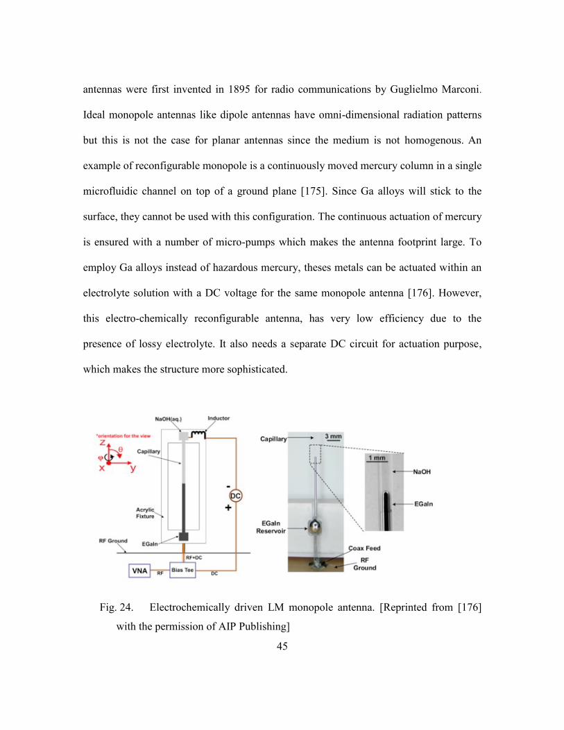
Fig. 24. Electrochemically driven LM monopole antenna. [Reprinted from [176] with
the permission of AIP Publishing] ............................................................................ 45
Fig. 25. Stretchable patch antenna with meshed structure (a) schematic, (b) optical
image of antenna and its transmitter (Reprinted from [178] with permission of John
Wiley & Sons, Inc.), (c) planar inverted cone antenna [Reprinted from [130] © 2009
IEEE] and (d) unbalanced loop antenna [Reprinted from [179] with the permission
of AIP Publishing] .................................................................................................... 48
Fig. 26. Multi-layer patch antenna. [Reprinted from [129] © 2012 IEEE] ................ 49
Fig. 27. (a) Unstretched and (b) stretched microstrip patch antenna. [Reprinted from
[162] © 2011 IEEE] .................................................................................................. 49
Fig. 28. (a) Meandered EGaIn lines used as a strain sensor. (b) Applying strain
changes the resistance of the conductor. (c) the sensor can be stretched up to 100%.
[Reprinted from [110] with permission from John Wiley & Sons, Inc.] .................. 51
Fig. 29. (a) Ideal coaxial transmission line, (b) a simplified configuration of coaxial
wire, (c) Real hand woven configuration of the fabricated coaxial line. [Reprinted
from [140] with permission from John Wiley & Sons, Inc.] .................................... 52
Fig. 30. Hybrid microfluidic LM electrode system. This concept has been used in
micro-coulter counter design [188]. Inspired from [166]. ........................................ 53
Fig. 31. Directing LM to: (A) and (B) one outlet, (C) and (D) two outlets, and (E) and
(F) three outlets with electrorecapillarity. Precise control of LM flow is not possible.
[Reproduced from [200] with permission from Royal Society of Chemistry] ......... 58
xiii
Fig. 32. (a) Fabrication process of LM electrodes with cylindrical posts, and (b) an
optical image of the actual electrode. [Reproduced from [166] with permission of
Royal Society of Chemistry] ..................................................................................... 59
Fig. 33. LM filling of a microstrip patch antenna. Most of the spacing between
PDMS posts are not filled with LM. [Reprinted from [129] © 2012 IEEE] ............ 61
Fig. 34. (a) LM flow stopped at valves’ entrances, and (b) passes through the valves.
Although the pressure has reached its critical value for valves, most of the gaps
between posts are not filled with LM. [Reproduced from [174] with permission of
AIP publishing] ......................................................................................................... 61
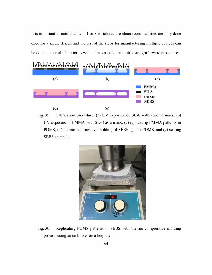
Fig. 35. Fabrication procedure: (a) UV exposure of SU-8 with chrome mask, (b) UV
exposure of PMMA with SU-8 as a mask, (c) replicating PMMA patterns in PDMS,
(d) thermo-compressive molding of SEBS against PDMS, and (e) sealing SEBS
channels..................................................................................................................... 64
Fig. 36. Replicating PDMS patterns in SEBS with thermo-compressive molding
process using an embosser on a hotplate…………………………………………...64
Fig. 37. The pressure measurement test set-up. ......................................................... 67
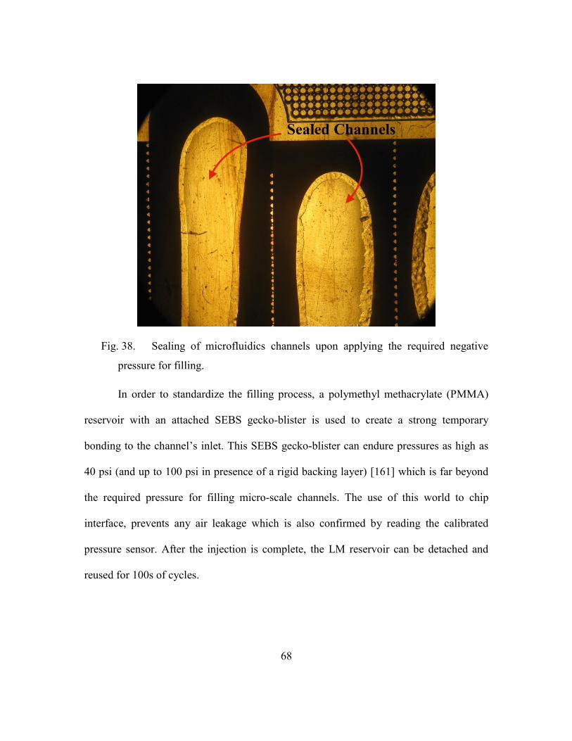
Fig. 38. Sealing of microfluidics channels upon applying the required negative
pressure for filling. .................................................................................................... 68
Fig. 39. (a) Schematic view of the stick-n-play PMMA chip with attached gecko
blister, and (b) filling of a power divider with this temporarily bonded filling chip. 69
Fig. 40. Optical photograph of the microchannels while filling with LM. The flow
merges the LM pinned between the posts in the nearby channel. ............................ 70
Fig. 41. The average critical pressure of EGaIn for filling microchannels made of
SEBS (Kraton® G1657) as a function of channel dimensions……………………..71
Fig. 42. Top-down optical image of EGaIn with SEBS channel walls for determining
the contact angle. ...................................................................................................... 72
Fig. 43. LM filled microstructure consisting of a straight channel and a delay
channel. (a) LM fills the straight channel and stops at the micro-valves, (b) and (c)
xiv
delay channel fills, and (d) fully filled structure and magnified view of micro-
valves……………………………………………………………………………….73
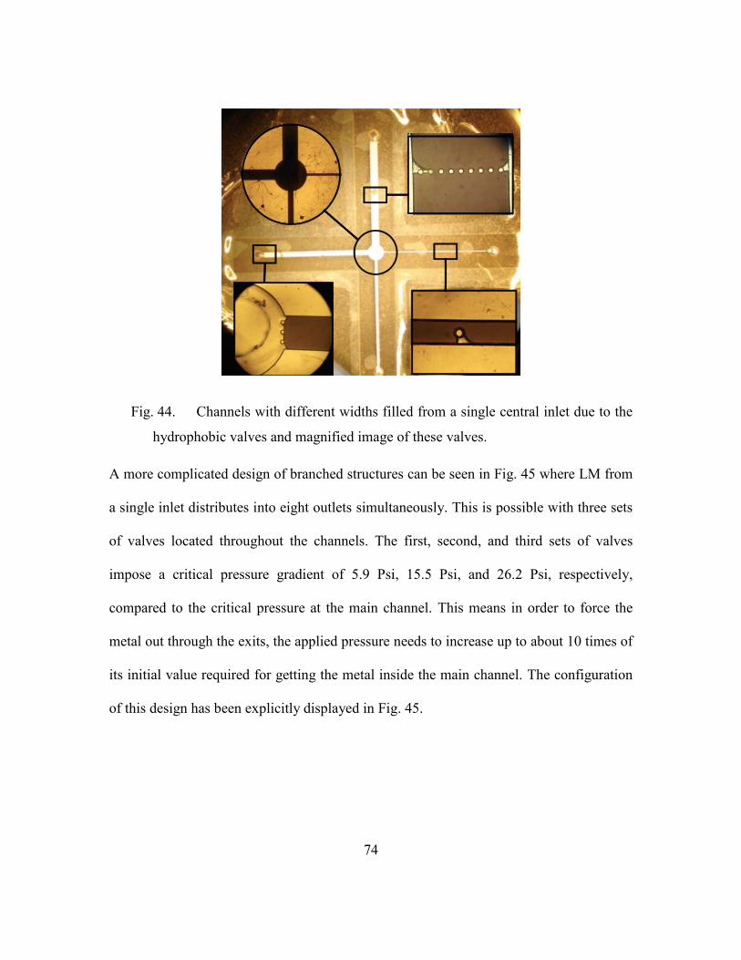
Fig. 44. Channels with different widths filled from a single central inlet due to the
hydrophobic valves and magnified image of these valves. ....................................... 74
Fig. 45. (a) Empty channels, (b) first round of barriers block the flow of LM after
being divided between two arms, (c) LM stops at the second arrangement of
triangular posts, (d) all the eight outlets are filled with EGaIn, (e) magnified photo of
the triangular pillars preventing LM flow, and (f) locating the valves within the
system. ...................................................................................................................... 75
Fig. 46. Filling strategy for low aspect ratio structure divided to narrower traces. W1
is the width between two parallel channels and W2 is the spacing between the
pillars………………………………………………………………………………..78
Fig. 47. Same channel filled in the designed and reverse direction: (a) LM enters the
gap between posts when it is filled in the designed direction, (b) air pockets are
trapped when system is filled in the reverse direction (The channel next to the
narrow part of the gaps is filled first). ....................................................................... 77
Fig. 48. (a) An entirely filled gap, (b) the gap is filled but the air pocket exists
underneath the metal, (c) the gap has not been filled with LM. ............................... 77
Fig. 49. Percentage of the gaps filled with lm versus the pressure difference for filling
the gaps’ space compared to the main channel. ........................................................ 78
Fig. 50. Creating isolated features from a monolithic LM trace with diluted HCl
injected from micro nozzles. (a) the trace before injecting HCl, (b) magnified view
of metal retracting due to the presence of HCl, (c) LM is pinned to the circular post
where further withdrawal of LM is avoided, and (d) final arrangement after 24
hours… ...................................................................................................................... 79
Fig. 51. (a) Bow-tie antenna structure before HCl injection, (b) using HCl and micro
posts, the device has been cut in half to create a bow-tie antenna, and (c) the final
device placed on human’s skin. ................................................................................ 80
xv
Fig. 52. Half bow-tie: (a) with straight guiding posts, and (b) with curved posts to
reduce sharp angles and air escapes. ......................................................................... 81
Fig. 53. (a) Kraton® G1657 pellets and (b) molded SEBS sample for measuring
electrical properties. .................................................................................................. 85
Fig. 54. Top view and side view of the folded dipole antenna. All the dimensions are
in millimetre. [Reprinted from [91] © 2016 IEEE] .................................................. 87
Fig. 55. SEM image of the folded antenna micro-channels along with the magnified
view of the adhesive micro-pillars surrounding the channels’ gasket. [Reprinted
from [91] © 2016 IEEE] ........................................................................................... 87
Fig. 56. (a) Exploded view of the flexible multilayer dipole fabricated with a single
injection step and (b) its dimensions. ........................................................................ 89
Fig. 57. Optical image of the multi-layer folded dipole and magnified images of its
alignment marks, inlet and outlet, and via before lm injection. ................................ 89
Fig. 58. Configuration of the patch antenna, (TS= 0.4mm, TT= 0.1 mm, TM= 0.07
mm, WP= 12 mm, LP= 20 mm, Wf= 0.9 mm, Lf= 10 mm). ...................................... 90
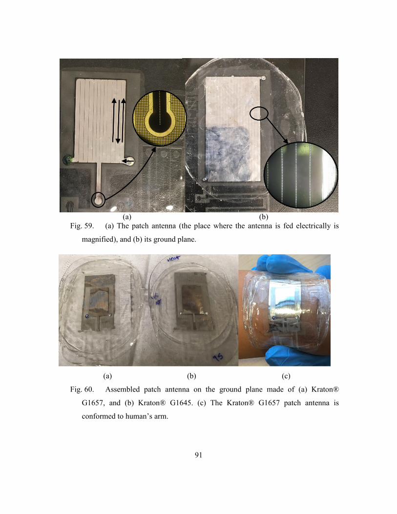
Fig. 59. (a) The patch antenna (the place where the antenna is fed electrically is
magnified), and (b) its ground plane. ........................................................................ 91
Fig. 60. Assembled patch antenna on the ground plane made of (a) Kraton® G1657,
and (b) Kraton® G1645. (c) The Kraton® G1657 patch antenna is conformed to
human’s arm.............................................................................................................. 91
Fig. 61. Releasing lm filled SEBS from glass without using acetone ........................ 92
Fig. 62. (a) Measuring the reflection coefficient on network analyzer, (b) zoomed in
image of the patch response on the screen, and (c) measuring the near field of
radiation pattern. ....................................................................................................... 93
Fig. 63. Simulated reflection response of the antenna for (a) variable length of dipole
axis when the matching axis has a constant length, and (b) variable matching axis
when the dipole axis is stretched to 160% of its original size. [Reprinted from [91] ©
2016 IEEE]................................................................................................................ 93
xvi
Fig. 64. Simulated and measured reflection response for different antenna sizes.
[Reprinted from [91] © 2016 IEEE] ......................................................................... 94
Fig. 65. Measured radiation pattern of the folded dipole at its center frequency
(5.5GHz). [Reprinted from [91] © 2016 IEEE] ........................................................ 95
Fig. 66. Reflection coefficient of dipole for different biaxial strains along the
matching and the dipole axes. ................................................................................... 95
Fig. 67. The measured radiation pattern at the center frequency of 4.875 GHz ........ 96
Fig. 68. Measured reflection coefficients of the stretchable antenna for different
strains.. ...................................................................................................................... 97
Fig. 69. Measured reflection coefficients of the stretchable patch antenna for 110%
stretch and different bending radii (BR). .................................................................. 98
Fig. 70. Simulated and measured co-polarization of E- and H-planes of the patch
antenna at its center frequency (4.8 GHz) ................................................................ 99
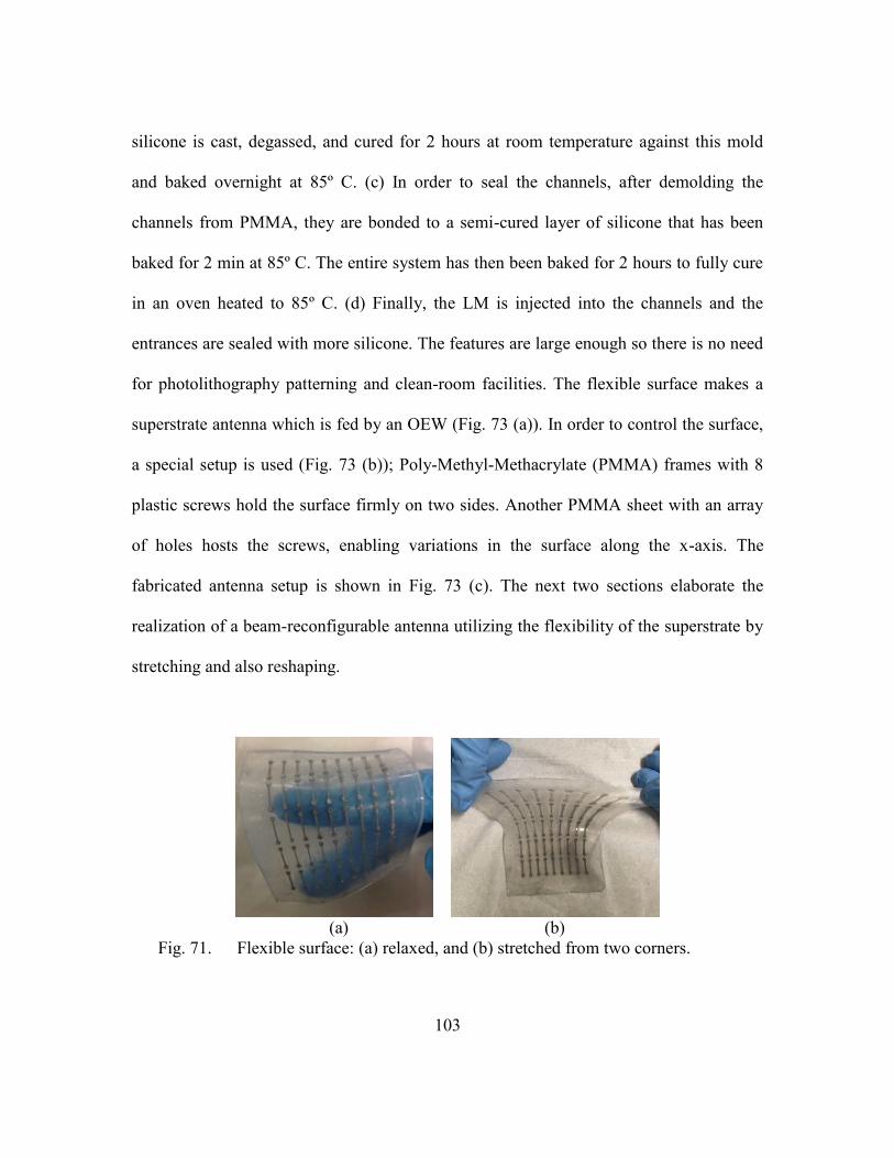
Fig. 71. Flexible surface: (a) relaxed, and (b) stretched from two corners. ............. 103
Fig. 72. Fabrication Process: (a) Fabricating PMMA mold, (b) Casting silicone
against PMMA, curing, and baking, (c) Punching the entrances and bonding the
channels to a semi-cured back layer, (d) filling the structures with LM and sealing
the channels. ............................................................................................................ 104
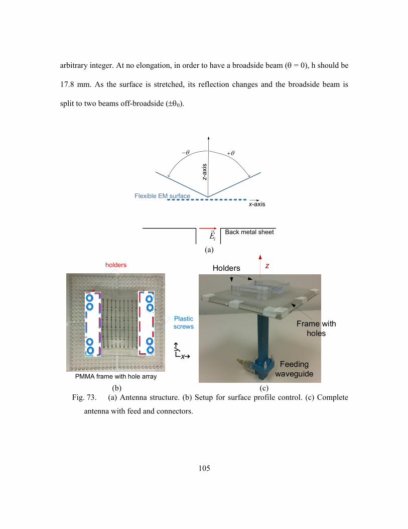
Fig. 73. (a) Antenna structure. (b) Setup for surface profile control. (c) Complete
antenna with feed and connectors. .......................................................................... 105
Fig. 74. Tuning the reflection of surface by elongation along x-axis. (a) Reflection
amplitude. (b) Reflection phase. ............................................................................. 106
Fig. 75. (a) Antenna inside NSI anechoic chamber. (b) Reconfiguration of radiation
pattern by stretching the surface. ............................................................................ 107
Fig. 76. |S11| of the antenna at different states mentioned above. ........................... 107
Fig. 77. (a) Reshaping the surface. (b) Convex state simulation model from side
view. (c) Convex state simulation model from top view. ....................................... 109
Fig. 78. Flexible surface in different reshaped states (a) concave side view; (b)
convex side view; (c) concave top view; (d) convex top view. .............................. 109
xvii
Fig. 79. Reconfiguration of radiation pattern by reshaping the surface at 12.5
GHz….. ................................................................................................................... 110
Fig. 80. L-edit design of the first mask for photolithography process. .................... 139
Fig. 81. L-edit design of the second mask for photolithography process. ............... 140
Fig. 82. The voltage-pressure relationship in calibration of the pressure gauge. ..... 141
Fig. 83. Randomly distributed residual Plot of the linear fit for ciritial pressure versus
(1/W+1/H). .............................................................................................................. 142
1
CHAPTER 1: INTRODUCTION
Microfluidics is the science of manipulation of fluids in micro-channels. Due to
its interesting features such as miniaturized sizes, laminar flow regime, lower costs, and
higher sensitivities, microfluidics has turned into an inseparable research tool in various
fields: molecular analysis, biology, optics, and microelectronics to name a few [1-3]. The
hope of applying silicon microelectronics techniques (such as photolithography) to
microfluidic electronics in order to drop fabrication costs and complexity has been one of
the driving forces in advancement of microfluidic electronics [4].
Flexible/soft electronics includes circuits and elements which can conform to a
desired configuration, different from their original shape. This technology often utilizes
soft and/or thin substrates instead of traditional rigid platforms to gain some degrees of
flexibility for purposes such as enhanced user experience in wearable electronics [5-6].
Stretchable electronics is a division of flexible electronics in which the system can be
elongated along one of the axes with a significant strain. Flexible/stretchable electronics
started mainly with applications in flexible displays [9-11], medical devices [13], body
worn electronics [14-16] [21], energy harvesting [17-18], and wireless power transfer
[23]. In stretchable microfluidic wireless communication devices, by reconfiguring the
physical shape of the elements (stretching, bending, twisting), their electromagnetic
radiation characteristics can be tuned to meet network variations. For this purpose, the
antenna structures are based on an elastic substrate with liquid conductor to provide
2
mechanical freedom that complies with surfaces such as human skin. In microfluidic
electronics, elastomers which are polymers with viscoelastic behavior are good
substitutes to traditional rigid substrates [5]. For the conductor, Eutectic Gallium Indium
(EGaIn) is commonly used in stretchable microfluidic electronics due to its attractive
properties such as decent conductivity and non-toxicity [7]. However, EGaIn is a non-
Newtonian fluid with complex behavior arising from a constantly forming oxide layer on
its surface when it is in contact with low levels of oxygen [8]. This gel-like liquid has
both the elastic (due to its skin) and viscous characteristics which makes it behave
unpredictably in micro-channels. For instance, although EGaIn has non-wetting
characteristics on most of the polymers due to its high surface tension, its skin sticks to
most of the surfaces and makes it stable. EGaIn can start to fill the microfluidic channels
when its pressure exceeds a minimum value where the oxide skin is broken. This pressure
depends on the dimensions and materials used for micro-channels.
Considering aforementioned discussions, the first objective of this thesis is to
characterize the unique properties of oxidized EGaIn LM and use them to enhance the
filling process of microfluidic channels. The goal is to achieve accurate control over the
pressure and sequence of filling in complicated structures such as branched, low aspect
ratio, multi-layered or discontinuous features. As a proof of concept, the second objective
is to design functioning stretchable antennas from simple one layer dipole to antennas
with multiple layers or complex geometrical configurations.
In Chapter 3, a cost effective and potentially mass manufactural fabrication
method based on SEBS thermoplastic elastomer is introduced for manufacturing
3
microfluidic platforms for stretchable communicational devices. This fabrication method
involves manufacturing of the gecko-adhesive pillars which provides a strong reversible
bonding around the micro-channels. In Chapter 4, functioning stretchable antennas are
designed, analyzed with FEM, fabricated, and tested. Chapter 5 describes the
manufacturing of a LM based shape reconfigurable frequency selective surface with
conventional microfluidics methods.
Overall, this thesis aims to provide a reliable, repeatable, and cost effective
solution for fabrication of complex mechanically reconfigurable microfluidic electronic
systems for soft-matter communicational devices.
4
CHAPTER 2: LITERATURE REVIEW
2.1 Flexible Electronics
Integrated circuits (IC) and packaging industry is constantly looking for methods
to shrink component sizes and investigate highly flexible and stretchable circuits that can
easily comply to complex surfaces [5]. In traditional rigid silicon-based electronics, there
is no opportunity for ergonomic design of biomedical electronic systems with excellent
user experience. Elastic substrates and flexible conductors revolutionized electronics in
the last decade. It is being predicted that electronics with flexible substrates will take
33% of the electronics industry market by 2022 [9].
There are three main elements for a flexible electronic device (also known as a
flex circuit [10]). They include the base material, the conductor, and the bonding
adhesive. The base filling material usually dictates the most primary mechanical and
electrical properties. The conductor may be thin films of metal, melted or LM, or
conductive non-metallic solutions. Bonding adhesive is required to assemble layers of
substrate matrix and it is possible to provide adhesion from the modified substrate itself
instead of a separate adhesive [11].
There are a number of unsolved challenges for commercializing flexible
electronics. These include finding a cost-effective and large scale manufacturing method,
exploring new design concepts for fabrication of large and multi-layered structures,
reliable sealing method and bonding improvement, standard and repetitive sub-processes
5
to name a few. In this section, we discuss methods and materials for flexible electronics
devices and applications of soft electronics.
2.2 Selection of Conductor for Flexible Electronics
2.2.1 Rigid Metals
Since the bending strains are a function of thickness, any material which is
sufficiently thin can be used in flexible electronics [12]. Such thin layers of metals can
mostly be bent non-destructively in order to reshape the device but they are not
significantly stretchable [13]. Embedding gold in silicone elastomers was one of the first
efforts to fabricate electronics with resolutions as low as 15 micrometers [14]. However if
the conductor needs to be thicker than a few microns, the high stresses would cause
fractures and ultimately electrical disconnection [15]. Utilizing spring/helical shape wires
in the elastomeric matrix instead of linear structures causes the metallic network to
deflect out of the plane while deformed [16]. This will make the principal stresses smaller
for a constant longitudinal strain. Pre-stretching the substrate prior to metal deposition
has been another technique for fabricating wavy conductors that can handle larger
amounts of strain before failure [17-18]. To achieve out-of-plane stresses for brittle
conductors there are three “wavy” material structures as shown in Fig. 1: out of the plane
wavy ribbon fully bonded to the elastomeric support, buckled wavy ribbon bonded to
elastomeric support only in specific locations, and in plane meshed ribbon [19].
6
Fig. 1. Three wavy material structures to enhance stretching of brittle conductors:
a: out of the plane wavy ribbon fully bonded to the elastomeric support, b:
Buckled wavy ribbon bonded to elastomeric support only in specific locations,
and c: in plane meshed ribbon [19]. [Reprinted by permission of John Wiley &
Sons, Inc.]
Apart from gold, reconfigurable wavy nanomembranes can be made from silicon,
which is inherently a brittle material, in a PDMS substrate [20]. Silicon and thin films of
transparent oxides such as ZnO are being used as semi-conductor in flexible electronic
devices such as transistors as well [21-26]. A stretchable patch antenna with capability of
sustaining 15% strain realized by screen printing silver nanowires in PDMS is another
example of flexible electronics with solid conductors [27]. The maximum strain reached
before failure for solid conductors is only up to 100% in the case of using multiple
parallel narrow traces instead of one single trace as shown in Fig. 2 [13][28]. Such
tortuous traces limit the design of electrical elements to simple transmission lines with
unnecessarily high inductances. Besides, fatigue failure is another disadvantage of these
7
types of conductors for long-term applications under repeated loading and unloading
cycles [29].
Fig. 2. Strain distribution in a multi-track conductor design. [Reprinted from [28]
with permission from Elsevier]
2.2.2 Conductive Polymers
Conductive particles such as metals or carbon embedded in an elastomer as the
filling material can form conductive polymers [30-31]. Several conducting particles such
as carbon black, silver, and nickel nanoparticles have been used in elastomeric matrix
among which single walled carbon nanotubes in a rubber matrix provides better
stretchability and conductivity [10][32-34]. Overall, these conductors have been used
mostly for fabrication of soft connectors, however, their electrical conductivity is very
low compared to their counterparts and their electrical characteristics change
considerably with strain [12][31]. Besides, they are not able to fully conform to the
8
surrounding environment due to the stretchability constraint of conductive polymers and
rigid metals [35-36]. For these reasons, tortuous wires are usually preferred over
conductive polymers for flexible electronics with considerable levels of deformation [13].
2.2.3 Liquid Conductor
Due to the aforementioned drawbacks of solid and particle conductors, fluidic
conductors have become very popular over the last decade. Fluids have nearly zero shear
modulus [37], therefore they can freely deform following the shape of substrate they are
encapsulated in. This along with their generally higher conductivities and the fact that
they have little hysteresis behavior, make them ideal substitutes for solid conductors. The
most common liquid conductor in traditional microfluidics has been electrolyte solutions
[5]. But their insufficient conductivity makes them inappropriate for radio frequency (RF)
systems. Other fluidic conductors such as water have been used for simple monopole
antennas, but they suffer from low conductivity [38] as well as the high evaporation rate
issue [39]. LMs have higher conductivities and are more stable in standard conditions.
Fabricating micro-scale structures with low temperature melting solders have been
practiced to achieve flexible electronic systems. The first attempt for stretchable
electronics originated from a strain sensor made of mercury in rubber tube [40]. Because
of its toxicity, mercury has been replaced in electronic industry by indium, tin and
gallium LM alloys [41-44]. In the following section, some of the most popular LMs and
their unique properties are discussed:
9
2.2.3.1 Common Liquid Metals
Mercury (Hg) is perhaps the most well-known room temperature LM. It was
widely used in the conventional thermometers, barometers, switches, and gauges. Despite
its availability and ease of use, its health threatening toxicity and large surface tension
has lead scientists to look for an alternative liquid conductor [45]. Gallium (Ga) and its
alloys are considered to be a promising replacement for mercury in electronic
applications. Ga is an non-toxic metal with a melting temperature of about 30º and a low
vapor pressure which makes it safe to work with by reducing the risk of inhalation [46].
Also, this low vapor pressure increases the durability in long-term applications due to the
small evaporation rate. This is especially important in micro/nano-scale manufacturing
since the evaporation rate per volume is relatively high in these scales. To further bring
down the melting point, eutectic gallium indium (EGaIn) is realized based on freezing
point depression principle. EGaIn consists of 75% Ga and 25% In by weight and has a
melting point of 15.5 [47]. Its interesting properties such as good electrical conductivity,
low melting temperature, biocompatibility, and mobility makes it a compelling material
for fabrication of flexible electronics. Galinstan is another alloy of gallium and is
composed of gallium, indium and tin. Its melting temperature depends on the mixing
ratio of its components. A typical composition is 68.5% Ga, 21.5% In, 10% Sn and has a
melting temperature of -19° C [10]. By changing the composition to 62.5% Ga, 25% In,
and 12.5% Sn, the melting temperature to shifts to 10° C [48]. Although conductors such
as galinstan and EGaIn have a conductivity of 10 times lower than copper, since the
10
depth of microfluidic channels is higher than the typical thickness of copper sheet, the
overall sheet resistance will be sufficient according to equation 1 [49].
Eq.1
In which is the sheet resistance, is the conductivity, and t is the thickness. The
properties of common LMs have been compared in Table 1.
Table 1: Comparison of LM Conductors
Liquid Metal Gallium EGaIn Galinstan Mercury
Surface Tension (N/m) in
Ambient Conditions
0.680 [45] 0.624 [50] 0.718 [51] 0.428 [52]
Viscosity (cSt) 0.34 [53] 0.32 [8] 0.37 [54] 0.11 [54]
Melting Temperature (ºC) 29.77 [55] 16 [47] -19 [54] -39 [54]
Electrical Conductivity
( S/m)
0.37 [55] 0.34 [56] 0.38 [54] 0.10 [54]
Boiling Temperature (ºC) 2205 [55] >1000 [49] >1300 [57] 357 [54]
Vapor pressure (Torr)
@ 30 ºC [45]
<
@ 300 ºC [58]
<
@500 ºC [57]
0.27
@100 ºC [45]
Density ( ) 6.1 [53] 6.3 [49] 6.4 [54] 13.5 [54]
11
2.3 Ga-based Liquid Metal Characteristics
2.3.1 Oxidization
When gallium and its alloys are exposed to oxygen levels above 1 ppm [41], a
very thin oxide layer forms on their surfaces. X-ray photoelectron spectroscopy shows
that Ga2O3 is the most stable form of Ga on the skin, however the existence of other
forms such as Ga2O is also demonstrated [59-60]. The atomic ratio of In:Ga:O at the
surface is 1:15:17 [8]. This dull looking oxide skin is composed of only a few monolayers
(with a thickness of 1-5 Aº [60-61]) and its thickness does not change over time [62]
since the previously formed oxide layer acts as a barrier to stop oxidization of the
underneath layers [60][63]. However, when the humidity level rises, an increase in the
metal’s viscosity has been observed. This increase in viscosity is correlated with the
oxide skin growth and accumulative amount of oxygen in the metal [63]. Also in humid
conditions unlike dry conditions, the oxide film thickness is dependent on the exposure
time to oxygen[63].
When LM fills into channels made of permeable PDMS, the oxide skin is formed
on the walls of channels as well as the front meniscus and the LM has a laminar flow
within this thin oxide layer [64]. The presence of the oxide shell on the walls is justified
by the fact that LM retracts at a slow pace after removing its meniscus’s oxide skin (with
acid/base/electrical current) rather than an immediate retraction [65].
This oxide layer determines the behavior of Ga alloys and alter some of its
characteristics. Although the LM has a very large surface energy and low viscosity, this
12
passivating skin [66] decreases the surface tension of LM [67] and stabilizes the LM
microstructures [8]. Measurements show that the surface tension of EGaIn changes from
624 (dynes/cm) in ambient environment to 435 (dynes/cm) when the oxide layer is
removed with dilute hydrochloric acid (HCl) [8][56]. Since moldable structures in LM
can be made only in micrometer to millimeter scale, the moldability of LM depends on
the surface area to volume ratio, and is attributed to the oxide layer which has a much
higher surface energy than the bulk LM [8]. This moldability makes the fabrication of
mechanically stable structures using methods such as 3D printing or freeze casting
possible [42][68].
The oxide layer is electrically insulating [69] but due to its small thickness, it does
not influence the conductivity significantly [61]. However, when electrical current goes
through LM, the oxide thickness changes and this results in modification of the electrical
resistance [70]. This phenomenon is used in fabrication of soft matter memristors and
diodes [69].
The visco-elastic behavior of the oxide layer of EGaIn measured with parallel
plates rheometer determines that it has both the viscous and elastic natures (but mainly
elastic) for a wide range of strains. Since both the elastic and viscous moduli dramatically
drop after applying about 0.5 N/m stress, this value is assumed to be the critical surface
stress for yielding the oxide skin of EGaIn [53] and negligible resistance to flow [8].
Sometimes it is essential to get rid of the oxide layer, for instance to switch back
to non-wetting nature of Ga based LMs. The amphoteric oxide layer of gallium can be
13
eliminated in acidic (pH<3) or basic (pH>10) environments [71]. The reaction of gallium
and gallium oxide with NaOH has been shown in equation 2 and 3, respectively [9]:
Eq.2
Eq.3
When galinstan comes close to HCl vapor, Ga2O3 and Ga2O change to GaCl3
and lnCl3 and in this reaction water is released [72]. Another way to get rid of the oxide
layer is by working in a sub-ppm oxygen conditions. However, achieving and
maintaining this low oxygen environment is a complicated and costly process [73].
2.3.2 Contact Angle and Wetting
Contact angle is defined as the angle between solid-liquid, solid-gas, and liquid-
gas at the contact line when these immiscible phases meet and is a function of interfacial
energies among these phases [74]. This thermodynamic property explains the wetting
properties of a liquid on a solid surface. The static contact angle can be expressed with
Young’s equation:
Eq.4
Where LV, SL, and SV are the surface tension of liquid-vapor, solid-liquid, and solid-
vapor interfaces respectively, and is the static contact angle. For the intended LMs, the
surface tension is very high and this results in a contact angle of higher than 90 degrees.
14
This means that mercury and Ga alloys without the oxide skin, have little wetting
characteristics which makes their actuation easier.
(a) (b)
Fig. 3. Contact angle of a liquid droplet on solid surface (a) without and (b) with
the external forces.
In the presence of external forces such as electro-static force or gravity, droplet
will move along a surface and dynamic contact angles are used instead. The dynamic
contact angle includes advancing/receding contact angles and sliding contact angle [75].
The Young’s equation describes the contact angle only on flat surfaces. For a
textured surface, the Wenzel model is used to describe the contact angle [76-77].
Eq.5
In which W is the apparent contact angle, r is a roughness factor (the ratio of actual area
of the surface to equivalent area of a flat surface). However, for a dual-scale surface
(micro/nano) it is maybe possible for the liquid droplet not to penetrate the nanoscale
structures and make the surface fully wet, therefore Wenzel model is not suitable
anymore and it is stated by Cassie state [78]. Cassie-Baxter equation extends the Wenzel
model for a composite surface [79].
Eq.6
15
Where F1 and 1 are the area fraction and contact angle of liquid on the component 1 of
the surface, and F2 and 2 are for the component 2 of the surface, and is the Cassie-
Baxter contact angle. Since for a LM droplet on a dual-scale surface, it may
not penetrate the nanocavities as shown in Fig. 4, the second component of the surface in
which the LM is in contact with is air therefore and the equation 6 changes to [76].
Eq.7
In this equation, Fs is the solid fraction which is in contact with the liquid, and c is the
Cassie-Baxter contact angle. This equation implies by making surfaces with small Fs, it is
practical to have super-lyophobic surfaces that LM does not wet them. This concept has
been used in the following sections for designing anti-wetting surfaces [80-81].
(a) (b) (c)
Fig. 4. LM droplet on (a) smooth surface (Young’s state), (b) on micro-textured
surface where wets the surface completely (Wenzel state), and (c) Dual
micro/nano-textured surface where it cannot penetrate into nanostructures
(Cassie-Baxter state)
Gallium, EGaIn and galinstan which have high non-wetting characteristics (high
contact angles) before oxidation, stick and wet most of the surfaces once oxidized
[67][82]. The very high adherence of Ga based alloys to most of the surfaces is attributed
to the oxide layer on their surfaces [45]. There are two modes of adhesion between the
16
oxide layer and the substrate [83]: 1. if the oxide skin is not ruptured before contacting
the surface a solid to solid contact happens which has a relatively low adhesion, and 2. if
the oxide layer is ruptured and a composite interface of old oxide skin (rough), newly
formed oxide skin (smooth) and bare LM is formed. This smooth new oxide layer
contributes to the increase in the contact adhesion. This high adherence to most of the
materials makes the actuation of LM within channels challenging and leaves residue on
the substrates after retracting the metal [83]. On the other hand, LMs without this sticky
skin such as mercury retract form channels immediately after removing the pressure and
tend to bead up [10].
2.3.3 Laplace Pressure
The pressure difference across the boundary of two immiscible matters or across
the interface of a curved surface is determined with Young-Laplace equation:
(Nm^-2) Eq.8
where n is the unit normal vector pointing out of the surface of interface, H is the mean
curvature, R1 and R2 are the principal radii of curvature, and is the surface tension. For
a rectangular channel we have:
Eq.9
17
In which W is the width and H is the height of channel, and is the contact angle
of liquid on the channel walls. Since the selected LMs have great surface tension values,
the Laplace pressure is high for them. The LM wets a microfluidic channel as soon as the
applied pressure in the upstream surpasses the Laplace pressure imparted by the channel
geometry on the liquid.
2.4 Handling of Liquid Metal
Handling of LM is very challenging due to the presence of its oxide layer which
makes it tricky to manipulate within micro-channels without leaving residue. However,
without a reliable method of manipulation, fabrication of electronic devices with
embedded LM is not feasible [78]. To overcome this problem, there have been a number
of attempts to lower the wetting characteristics of LM by modifying either the
LM/substrate or by preventing their direct contact. In this section, we discuss about
different methods for handing Ga based LMs.
2.4.1 Using a Carrying/Lubricating Solution
To reduce the super-lyophilic nature of oxidized LM on substrates, it is
sometimes manipulated within a lubricating solution. Teflon solution, deoxygenated
silicon oil, polyethylene glycol (PEG), and polyvinyl alcohol (PVA) have been used to
prevent the surface of channels from getting stained with LM residue [7][82-85].
Furthermore, channels prefilled with some liquids like glycerol or water lubricate the
flow of LM by creating a slip layer between the oxide and the channel’s walls. Water
18
brings down the critical yield stress by weakening the oxide layer as well [86-87].
However, manipulating the LM within another solution can interfere with the movement
of LM for some applications and it is not practical all the time. Such issues are discussed
in detail in the following sections.
Fig. 5. Water slip layer. [Reprinted from [86], Copyright 2016 American
Chemical Society]
2.4.2 Liquid Metal Oxide Layer Removal
If the oxide layer of Ga alloys is removed, it behaves like a Newtonian liquid and
therefore its accurate manipulation is feasible in micro-scale. Acids with pH lower than 3
such as diluted hydrochloric acid have been widely used for enhancing LM manipulation
in various applications [56][72][88]. This concept has been used in preparation of
microfluidic channels made of papers that are previously impregnated with HCl for easy
manipulation of oxidized galinstan [89]. PDMS is also extremely permeable to HCl
vapor. This thickness dependent permeability is used for surface reduction of galinstan as
shown in Fig. 6. Two parallel channels, one filled with LM and the other one filled with
19
37% wt HCl, are separated with a 200 µm thick PDMS wall. The HCl vapor diffuses
through the PDMS to react with the oxide layer on the galinstan surface [90]. The high
volatility of HCl, however, can damage the electronic components [78] especially in
highly permeable substrates such as PDMS [78]. Therefore, it may be beneficial to use
less permeable substrates such as styrene-ethylene-butylene-styrene (SEBS) in
applications where microfluidic channels need to be filled with HCl to reduct Ga oxide
layer [91].
Fig. 6. On chip HCl treatment of galinstan droplets. [Adapted from [90] with
Permission from Royal Society of Chemistry]
20
2.4.3 Lyophobic Coating of LM Droplets
Coating LM droplets with nanoparticles such as WO3, TiO2, MoO3, In2O3, teflon
powder, silica, and carbon nanotubes enhances the non-wetting characteristics of LMs
[92]. These LM marbles have very high contact angles on various substrates, however
this method is limited only to LM droplets.
2.4.4 Substrate Surface Modification
Another method to overcome the high adherence of LMs, is to modify the
substrate’s wetting properties. This can be done by physically texturing the substrate with
the use of deposited particles or by using chemicals to micro-machine the surface.
2.4.4.1 Physical Method
Inspired by super-hydrophobic lotus leaves due to their dual scale texture, a
PDMS surface can be modified to improve the non-wetting characteristics of oxidized
LM as well. This is possible by transferring the micro-nano dual scale textures of another
substrate (such as paper) to PDMS walls. By coating these textured channels with
titanium oxide TiO2 nano-particles, the advancing and receding contact angles of
galinstan on PDMS increases from 130° and 9° to 167° and 151°, respectively [78]. The
reason for this high contact angle growth is the transfer of nanoparticles to LM droplets
from the PDMS channel walls which produces LM marbles. Imprinting carbon nanotubes
grown initially on Si on PDMS also generates an anti-wetting surface for oxidized
gallium oxide due to the its mixed micro-nano scale morphology [93].
21
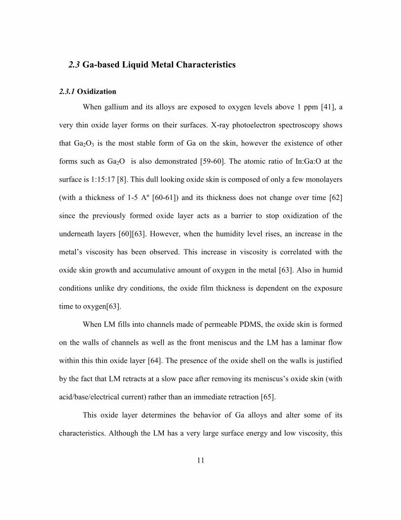
In another study PDMS patterned with an array of micro-pillars is used for
fabricating microfluidic channels as shown in Fig. 7. By changing the pillars pitch
distance, from very large values to small values, the wetting changes from Wenzel state
(completely wetting the surface) to Cassie state (complex air, liquid and solid interface)
[94-95].
Fig. 7. (a) Cross section of super lyophobic micro-channel, (b) Galinstan flowing
through the channel. [Reprinted from [94] © 2012 IEEE]
2.4.4.2 Chemical Method
Strong inorganic acids such as sulfuric acid H2SO4 are used for making dual-scale
structures in PDMS channels by attacking the surface of channels. HF and HNO3 have
also be used to texturize PDMS, H2SO4 however, seems more effective by increasing the
advancing contact angle to 167° and a minimum contact angle hysteresis of 14° [78].
Chemically machining of surfaces is a superior solution for increasing contact angle both
in terms of reliability and contact angle hysteresis [78].
22
Fig. 8. PDMS surface after being in contact for 1 min with (a) HF, (b) HNO3 and
(c) H2SO4. [Adapted from [78] with permission from Royal Society of Chemistry]
2.5 Methods for Patterning LM
In order to make functional devices made of LM, it needs to be patterned in a fast,
reliable, and accurate process. This step is equivalent to chemical etching process of
copper in PCB manufacturing. In this section, different methods for patterning Ga based
LMs, including additive and subtractive techniques, are discussed.
2.5.1 Additive Manufacturing
2.5.1.1 Masked Deposition or Stencil Printing
In this process the LM is deposited on the substrate through a contact mask. Once
the deposition is complete, the mask is removed either by etching or simply peeling off
and the patterned LM is left on the substrate. Afterwards LM needs to be frozen prior to
casting the next elastomer layer so the patterns do not distort in the casting and curing
process. The final substrate is usually semi-cured prior to LM deposition so that it can
bond to the sealing layer later on. The resolution of this method mostly depends on the
stencil’s resolution and has been as low as 50 microns for a copper stencil patterned with
23
ultra violet (UV) lithography, however the surface roughness is still significant as shown
in Fig. 9 [96]
Fig. 9. (a) Front and (b) back side of copper stencil, and (c) patterned galinstan on
PDMS. [Reprinted from [96] with permission of Royal Society of Chemistry]
The stencil can be made with laser machining or 3D printing if there is no need
for accuracy [97]. To have higher resolution and smaller features the stencil is fabricated
with photolithography process [98]. However even in these cases, the actual widths
sometimes differ by 50% due to the aggressive etching of the stencil [99]. Moreover,
there is no means of accurate height control in the existing literature.
2.5.1.2 Micro-contact Printing or Stamp Lithography
Micro-contact printing has been practiced for years as a parallel soft lithography
method [100] but it was not until recently [101] that it was used for printing of LMs. In
this method, a relief pattern on the stamp (made of different materials such as PDMS) is
inked with LM (either by dipping into ink pool or brushing the stamp) and places the LM
on the final substrate. When the pattern is printed entirely, another layer of elastomer is
24
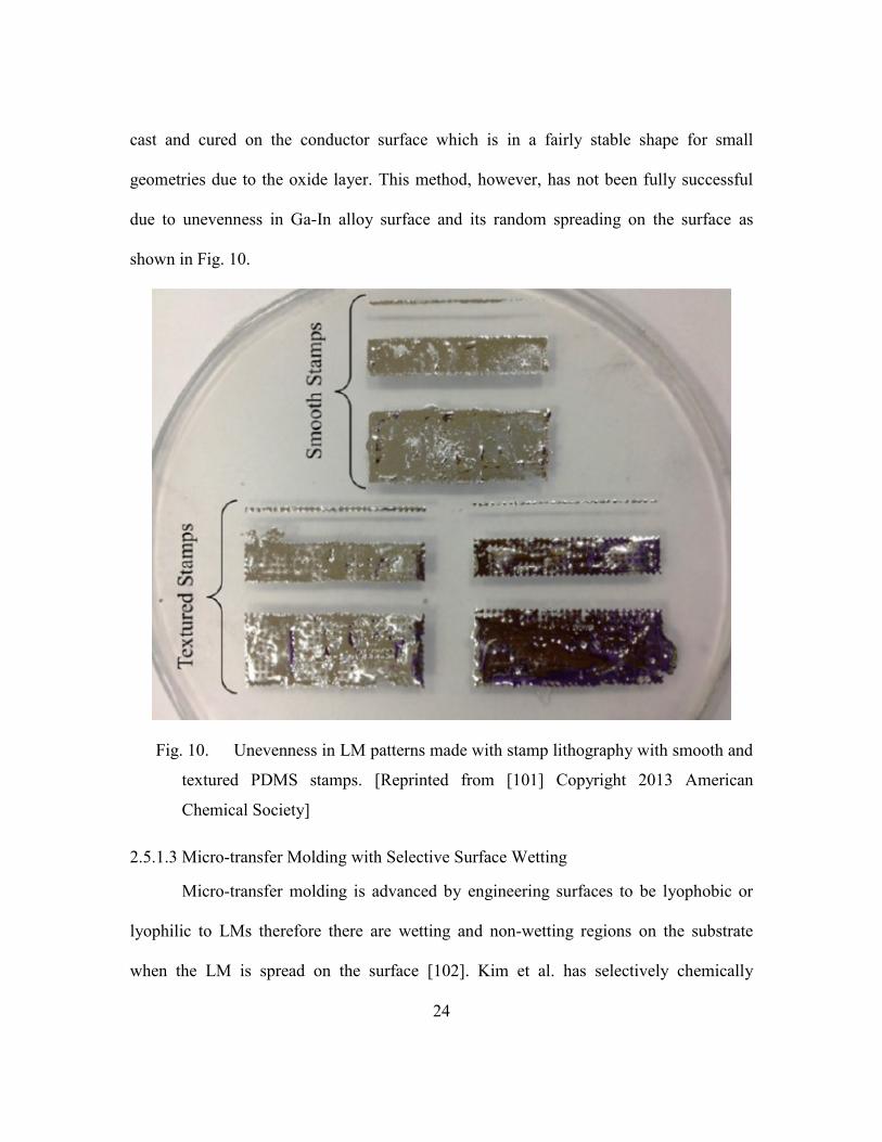
cast and cured on the conductor surface which is in a fairly stable shape for small
geometries due to the oxide layer. This method, however, has not been fully successful
due to unevenness in Ga-In alloy surface and its random spreading on the surface as
shown in Fig. 10.
Fig. 10. Unevenness in LM patterns made with stamp lithography with smooth and
textured PDMS stamps. [Reprinted from [101] Copyright 2013 American
Chemical Society]
2.5.1.3 Micro-transfer Molding with Selective Surface Wetting
Micro-transfer molding is advanced by engineering surfaces to be lyophobic or
lyophilic to LMs therefore there are wetting and non-wetting regions on the substrate
when the LM is spread on the surface [102]. Kim et al. has selectively chemically
25
modified the wetting properties of PDMS with toluene, therefore when the PDMS mold
is pressed against a LM film, the metal on the chemically modified parts can be easily
transferred to a sacrificial layer [103]. Li et al. has discovered that HCl treated galinstan
selectively wets patterned Au layer deposited on PDMS [104]. This approach provides a
good resolution but it needs deposition of Au and Cr layers and pattering them ( Fig. 11).
If the surface is not selectively engineered to enhance or deduct wettability, the LM
outside trenches needs to be cleaned afterwards by some methods such as acid treatment.
This is the underlying principle for imprinting patterning technique [105]
Fig. 11. Fabrication process of EGaIn structures in PDMS via Au selective
wetting. [Reprinted from [104] with permission from Elsevier]
2.5.1.4 Direct Writing (2D and 3D Printing)
LM structures can be directly-written at room temperature with pressures lower
than 5 kPa at micro-scale [106]. This method includes using advanced automatic 3-
dimensional (3D) printers with precise control of the position of nozzle [107] or simply
painting the LM on the substrate with a brush or a pen [108-109].
26
Fig. 12. A roller ball pen filled with GaIn24.5 alloy for direct writing. [Reprinted
from [109] with the permission of AIP Publishing]
Printing 3D free-standing structures (which are not supported by an encapsulating
layer) is more challenging and requires techniques such as piling droplets of LM or
injection molding into an elastomer and etching it later on as explained in Fig. 13 [106].
Otherwise if LM traces need to be encapsulated in an elastomer, they are frozen and
sealed with a curing polymer like in previous methods [110].
Yan et al. have developed a coaxial printing technique that simultaneously prints
the substrate (PDMS) and the LM core [111]. Although this method can be optimized
further for printing multi-dimensional shapes, it opens a new window for facile
fabrication of flexible electronics [111].
27
Fig. 13. Fabrication of LM free standing structures with: (a) Extrusion of LM from
a needle to write free standing wires, (b) Expelling metal rapidly with bursts of
pressure, (c), (d), (e), and (f) Stacking of droplets to form tall structures, (g)
Injection molding to PDMS micro channels and etching the channels later on with
tetrabutylammonium fluoride. Reprinted from [106] with permission from John
Wiley & Sons, Inc..
Fig. 14. Coaxial nozzle schematic for simultaneous print of conductor and
substrate. [Adapted from [111] with permission of AIP Publishing]
Two opposing factors to quality and resolution of direct writing methods are low
viscosity and large surface tension of LMs, however the oxide layer stabilizes the LM
28
structures to some extent if the size of the features are small enough [106]. On the other
hand, there is not any means of robust and accurate control of the dimensions yet and the
fabrication process is tricky [110]. The sizes of features that can be patterned in room
temperature LMs also is in a small range where they are not too small or too large to be
possible to print and to avoid yielding and collapsing [112]. Using additional steps along
with 3D printing such as freezing the printed metals on the fly can facilitate achieving
more stable 3D structures [113]. Furthermore, more research needs to be done on
obtaining reliable nozzle and printing set-up that does not corrode when in contact with
Ga alloys and can be cleaned.
2.5.1.5 Injection Molding and Vacuum Assisted Filling
Due to the very high surface tension of LM it is tricky to shape it in desired forms,
therefore it can be inserted into already-formed arrangements [114]. To force LM into
pre-sealed channels a positive pressure (injection molding) or negative pressure (vacuum
filling) can be used. This pressure should be higher than the critical surface tension of Ga
based alloys to break the oxide skin. For channels with larger widths this is a
straightforward process and can be done with a simple needle. However, when there is a
need for miniaturization of the system and to control the filling parameters (for instance
in measuring filling pressure) a reliable and repeatable chip to world connection should
be used. Despite its simplicity this method has limitations for complex 3 dimensional
structures with multiple inlets and outlets [106].
Laplace pressure shaping is another filling technique that takes advantage of
vacuum for patterning [6]. Cumby et al. fabricated devices by inserting a LM droplet
29
between two sheets of patterned polymer (poly-ethylene terephthalate or polyimide) and
applying vacuum to evacuate the air and pulling the LM into holes [49]. For Ga based
LMs an inert gas like nitrogen, or HCl vapor which reacts with metal oxide needs to be
used to avoid formation of gallium oxide which makes this process less practical [49].
Another drawback is that as soon as the vacuum is released, LM retracts from the
channels if not fixed in the traces by some approaches such as freeze-casting [6].
(a) (b)
Fig. 15. Patterning LM structures with Laplace pressure shaping method. (a) The
LM droplet is placed between two elastomer layers. (b) When the vacuum is
applied metal droplet is pushed into trenches. Inspired from [49].
2.5.1.6 Ink Jet Printing or Jetting
Despite several proposals for inkjet printing of Ga based metals, this patterning
method is not trouble-free for these alloys. Jetting with Ga alloys, if not performed in an
oxygen free environment, leads to accumulation of oxidized LM at the nozzle [101]
[115]. To avoid clogging and oxidizing, the orifice of the printing system (made of
PDMS) can be fabricated from HCl impregnated paper [116] but this method is far from
a long-term and reliable method of patterning.
2.5.1.7 Tape Transfer Atomization Patterning
In this method liquid alloy is atomized and sprayed on a half cured PDMS substrate
through a tape transferred mask and then encapsulated as shown in [117]. Semi-cured
30
PDMS will improve LM wetting on the PDMS surface so that the patterned metal
remains in place when the mask is removed [118]. This method is a potentially large
scale manufacturing method but it lacks resolution and the line roughness is high.
2.5.1.8 Freeze Casting: A Complementary Method in Additive Manufacturing
It is often necessary to maintain LM structures’ shapes before sealing them within
another layer of elastomer in additive manufacturing methods like direct writing, micro-
contact printing, masked deposition, and Laplace pressure shaping. Due to the large area
to volume ratio for micro-scale LM structures, the melting happens faster than usual and
the size discrepancy between the nominal and final sizes is observed [6][99]. The
elastomers that are molded after LM pattering need to be cured at low temperatures to
minimize the distortion of LM patterns. Since curing of most of the polymers such as
PDMS is temperature dependent, these methods work only for structures with low aspect
ratios where the oxide layer can preserve the melted LM’s shape to some extent [6]. For
taller structures in freeze casting and when it is essential to precisely control the height,
the frozen components should be placed manually in patterned molds as shown in Fig. 16
to avoid shape distortion [6]. However, if the structures are small, handling these small
pieces is extremely tough and requires accurate means of alignment. Another solution is
to use UV curable polymers to make the curing process faster while alloys remain solid.
For these reasons the resolution for most of the manufacturing methods that are based on
freeze-casting is as low as 200 micrometers [6].
31
Fig. 16. (a) General freeze casting process and (b) freeze casting for tall/complex
structures using patterned substrate and manually aligning pieces. [Reprinted from
[6] with permission form Royal Society of Chemistry]
2.5.2 Subtractive Manufacturing
2.5.2.1 Direct Laser Patterning
In this method, LM (EGaIn) is encapsulated between two PDMS layers but it is
not patterned until a CO2 laser locally heats PDMS. The heat from the laser vaporizes
PDMS in the bottom layer. This vaporized PDMS punctures the LM surface and
displaces the LM as shown in Fig. 17 [119]. This is a rapid prototyping method in soft
lithography however the resolution is about 150 micrometers, the roughness is
considerable and in cases where the conductor occupies a small ratio of area or where the
size of the device is large it is not efficient.
32
Fig. 17. Laser patterning fabrication process. (a) LM is sandwiched between
PDMS layers, (b) Bottom PDMS layer is locally heated and vaporized, (c) When
the vapour pressure exceeds the surfaces tension of metal ruptures the oxide layer
and (d) relocated the LM. [Reprinted from [119] with permission of John Wiley &
Sons, Inc.]
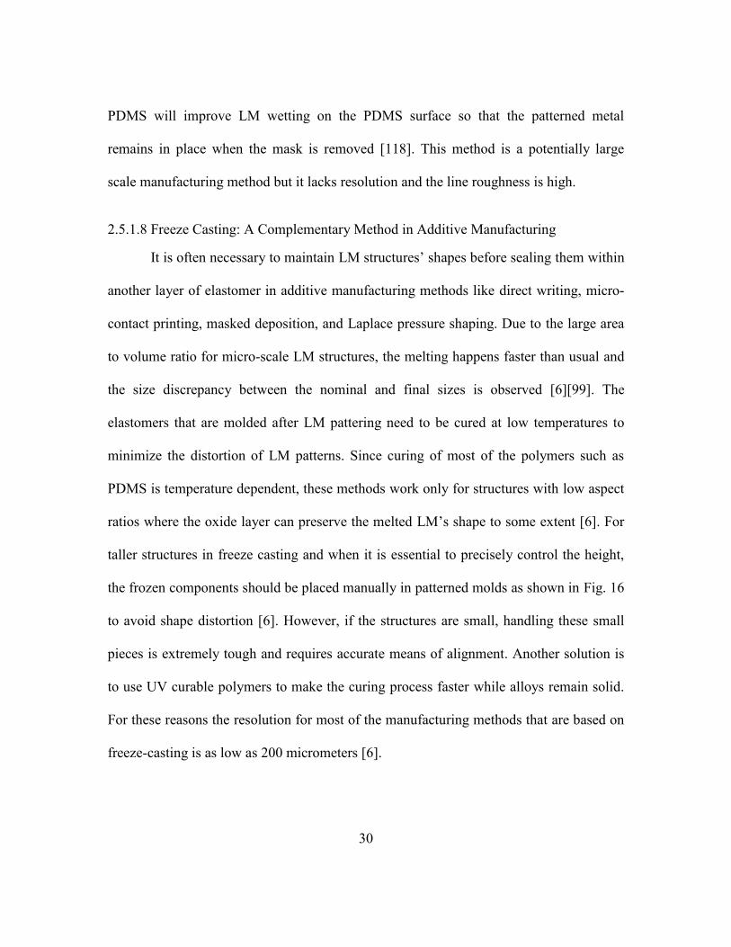
2.5.2.2 HCl Selective Erasure
In this method LM filled PDMS micro-channels are treated by inserting an HCl
droplet on top of the sealing layer. HCl vapor penetrates through top layer and dissolves
the oxide layer which causes LM to bead up and retract [120]. In spite of
reconfigurability arising from the fact that these structures can be filled again with LM,
33
precise control of the LM location is almost impossible and the method is inherently
slow.
Fig. 18. Array of closed ring resonators made of LM embedded in micro-fluidic
channels. Two rings have been emptied by HCl selective erasure method.
[Reprinted from [120] with the permission of AIP Publishing]
2.6 Selection of Substrate in Soft Electronics
A typically insulating substrate is required for encompassing soft conductors and
avoid their contamination. Synthetic and natural rubbers are the most used substrates in
flexible electronics due to their flexibility and low-cost. These flexible substrates serve as
dielectrics in radiating elements or just a packaging material in other applications.
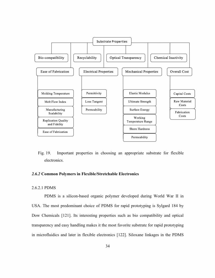
2.6.1 Important Parameters in Selecting a Substrate for Soft Electronics
The most important properties in choosing an appropriate substrate for electronic
devices are mentioned in Fig. 19.
34
Fig. 19. Important properties in choosing an appropriate substrate for flexible
electronics.
2.6.2 Common Polymers in Flexible/Stretchable Electronics
2.6.2.1 PDMS
PDMS is a silicon-based organic polymer developed during World War II in
USA. The most predominant choice of PDMS for rapid prototyping is Sylgard 184 by
Dow Chemicals [121]. Its interesting properties such as bio compatibility and optical
transparency and easy handling makes it the most favorite substrate for rapid prototyping
in microfluidics and later in flexible electronics [122]. Siloxane linkages in the PDMS
35
backbone gives it its great flexibility and stretchability. PDMS however, is a thermoset
polymer which cross-links into a 3-dimensional structure while curing and cannot be
heated to remold after being cured once. This makes it unsuitable for some industrial
mass production manufacturing methods such as hot embossing [123]. Another issue with
PDMS is its low surface energy which makes the bonding of PDMS layers challenging.
In order to seal microfluidic systems made of PDMS, adhesion strength needs to be
improved by some technologies such as oxidizing with oxygen plasma [124]. The
extensibility of PDMS depends on its grade and preparation method [125]. Sylgard 184
for instance has a Young’s modulus of 1.32-2.97 MPa, and an ultimate tensile strength of
3.51-7.65 MPa [126], but most of the devices composed of it fail well below 100% strain
values [127]. There are complex methods to increase this value to about 200% by
fabricating 3D nanonetworks in PDMS proximity field nanopatterning [128]. PDMS has
a dielectric constant in the range of 2.77-3.69 depending on its working frequency [5]. At
100 kHz, its dielectric constant is 2.67 and it changes to 3 at 3.45 GHz [129]. Its loss
tangent is 0.001 at 100 kHz [130] and shifts to 0.05 at 3.45 GHz [129].
2.6.2.2 Ecoflex®
Ecoflex® is a low viscosity bio compatible platinum catalyzed silicone and has
been on market since 1998 [131]. Its elongation at break depends on its grade and is up to
1000% for some classes of ecoflex®. This high level of stretchability and its water
resistivity makes it a fascinating substrate in fabrication of extra soft substrates especially
in epidermal electronics [132]. Ecoflex® comes in a two part formulation (precursors)
that need to be mixed for curing [133]. In spite of its attractive mechanical properties,
36
tough handling, optical opacity, high viscosity after mixing, and difficulty in bonding to
itself, keeps Ecoflex® away from being a commercial substrate in electronics industry
[134]. Ecoflex® has been used in academic labs for fabrication of antennas [135], sensors
[136-137], and circuit elements [101], however there is no record of its electrical
properties.
2.6.2.3 SEBS
Styrene ethylene butylene styrene (SEBS) is a triblock copolymer with high
tensile strength and low modulus [138]. SEBS consists of ethylene-butylene chains with
styrene domains on each end [123]. SEBS is available commercially (at lower costs than
PDMS) with the trade name of Kraton® with different polystyrene content which shifts
its mechanical properties and manufacturing parameters. SEBS is classified in a group of
polymers named thermoplastic elastomers (TPE). Thermoplastic elastomers have the
characteristics of both elastomers and thermoplastics and can be reversibly bonded to
surfaces. In thermoplastics, polymer chains associate with intermolecular forces. These
forces weaken dramatically above their melting temperature resulting viscous
characteristics of thermoplastic. That is why thermoplastics are compatible with mass
production methods such as extrusion or thermo-compressive molding and can be
recycled and reused unlike thermosets. Elastomers have both viscosity and elasticity
characteristics and very weak intermolecular forces which leads generally to low elastic
moduli and high strain before failure. Despite these interesting properties, with PDMS as
the dominating material for soft electronics, SEBS elastomer has been overlooked in this
37
industry. The application of SEBS has been limited to few cases where it is used as the
wire coating for liquid conductor wires [139-140].
2.7 Bonding Technique
A microfluidic channel needs to be bonded to another blank or patterned substrate
in order to keep the fluid/gas inside the chip. In spite of the advancements in
microfluidics manufacturing methods, bonding of microfluidic chips has still remained a
delicate and critical step [141]. Depending on the application, materials used, and desired
mode of failure, various methods of sealing may be utilized. In general, bonding
techniques can be categorized to reversible and irreversible bonding. A reversible
bonding allows multiple assembly and disassembly of the chip without damaging it. This
is beneficial for alignment purposes, temporary bonding applications, and recovering the
valuable fluids. Irreversible bonding techniques on the other hand, usually provide higher
adhesions and therefore can be used in high pressure applications [142]. This bonding
includes indirect bonding techniques such as adhesive bonding [143], or direct bonding
methods such as thermal fusion [144], localized welding [145], solvent bonding [146],
and bonding with surface modification [141]. Surface energy modification methods such
as plasma activated bonding are of the most common methods for bonding PDMS [147].
In plasma bonding, a plasma is created either with gases such as Ar, Ne, CO, He, N2,
NH3, H2O, CO2, and O2 or with air, or vacuum [148-149]. Plasma bonding however, is a
costly and time consuming process [147]. Another widely used bonding method
commonly used in polymeric electronics, is using an uncured or partially cured sealing
38
layer to achieve strong irreversible adhesion between the two layers yet the bonding
results are inconsistent with this method [147].
Elastomers like PDMS or SEBS can be reversibly bonded to themselves or other
materials by Van der Waals forces when they are in close contact. Van der Waals forces
are relatively weak intermolecular forces which arise from interaction of transient or
permanent dipoles. These forces can hold up to 5 psi fluid pressure and about 1 µl/min
flow rate in PDMS microfluidic channels [150-151]. The energy required to separate two
bodies which are in contact is called surface free energy and it depends on the effective
contact perimeter rather than contact area [152]. This can also be seen in the equation for
the pull off force for two elastic spheres in contact [153].
Eq.10
Eq.11
Where P is the pull-off force, is the energy per unit contact area, and R1 and R2 are the
radii of spheres 1 and 2. Since the pull-off force is correlated with the effective contact
perimeter, by splitting the contact surface dispersive adhesion can be increased. This
phenomenon is called the “gecko effect” and is used in designing patterned surfaces with
enhanced adhesion forces [154]. Geckos can adhere strongly to most of the surfaces by
attractive Van der Waals forces due to the spatula shaped setae on their toes [155]. These
hierarchical structures have inspired scientists to design biomimetic dry adhesives by
micro-structuring various thermoplastics and thermosets [156-158]. Campo et al. have
39
tested different shapes of pillars to optimize the adhesion strength including pillars with
flat, spherical, concave, spatular, and mushroom tips shown in Fig. 20 [159]. Their
experiments showed that mushroom shaped and spatular tip pillars attain maximum
levels of adhesion, which is about 30 times higher than the flat punch design [159].
(a) (b) (c) (d) (e)
Fig. 20. Different pillar shapes in dry adhesive design including: (a) flat punch, (b)
spherical tip, (c) concave tip, (d) spatular tip, and (e) mushroom shape tip.
Inspired from [159].
Carbone et al. have suggested that this superior adhesive performance in case of
mushroom shaped pillars is due to the elimination of stress singularity compared to flat
punch design which changes the detachment mechanism. However, when the the pillar
cap is too thin, a large stress concentration is observed, and when the cap thickness is too
high, the stress singularity reappears [160]. The distribution of stress along the cap
surface has been shown in Fig. 21. Wasay et al. used gecko-inspired dry adhesives for
microfluidics application for the first time [161]. A gasket which is a sweep of the
mushroom shaped pillars makes the microfluidics channels walls. Individual mushroom
shaped pillars are surrounding this gasket for enhanced reversible adhesion. For
microfluidic chips made of SEBS with a polystyrene backing layer, this bonding
technique can sustain up to almost 100 psi pressure which is 10 times higher than a
40
standard reversible bonding of PDMS [161]. Developing a reliable and reversible
bonding technique which does not put limit on stretchability of the substrate material, and
can handle great fluid pressures, is critical in reconfigurable microfluidic electronics and
is often the bottleneck point in evolution of super soft microfluidics electronics [162].
(a) (b) (c) (d)
Fig. 21. Stress distribution for a (a) flat punch pillar, (b) mushroom shape pillar
with thin cap, (c)mushroom shaped pillar with thick cap, and (d) mushroom
shaped pillar with optimum thickness of cap. Inspired from [160].
Other methods for reversible bonding of polymers include using vacuum assisted
bonding [163], bonding with magnetic clamping [164], and using external adhesives such
as double sided tape to name a few, however, these methods limit the stretchability and
versatility of the system.
2.8 Liquid Metal Based Devices
Ga-based liquid alloys can potentially be the next generation of conductors in soft
electronics. They have been used in fabrication of reconfigurable communicational
devices [39][130], interconnects [165], electrodes [166], RFID tags [167] and circuit
41
elements [101], to name a few. Soft electronic devices can be categorized to
reconfigurable and non-reconfigurable devices. To attain reconfigurability, three main
techniques are practiced:
Repositioning the liquid conductor with hydraulic or pneumatic manipulation
[168]
Elongating the system axially or biaxially [169]
Flexing and arching the system [170]
Actuating Ga-based liquid conductors in circuits is very challenging due to their
stickiness arising from the oxide layer. Removing the oxide layer with other methods also
causes unnecessary complications in the process. Arching/bending the device brings
nonlinearity and unpredictable results and is not practical for all applications. Therefore,
among the aforementioned reconfiguring methods, axial elongation is often preferred. In
case of non-tunable soft electronics, the flexibility only serves for an enhanced conformal
coating on curved or dynamically deforming surfaces especially in epidermal electronics
[171].
2.8.1 Antennas
Antennas are arrangements of conductors or apertures that provide a platform for
radiating or receiving electromagnetic waves by translating guided waves into free-space
waves. Antennas are categorized to four major groups based on their sizes and their
radiation mode:
42
Electrically small antennas: Operating wavelength is much larger than physical
size of the antenna.
Resonant antennas: Their physical size is in order of half wavelength.
Broadband antennas: Electrically large antennas which are continuously resonant.
Aperture antennas: The radiating wave flows through a physical aperture.
For wireless communications, depending on the application, the antennas need to
have certain properties in terms of distribution of power in space, polarization, impedance
matching, bandwidth, and efficiency. By reconfiguring these properties, a single antenna
can be used in different working points and this makes reconfigurable antennas extremely
vital in compact wireless power transfer systems [172]. This tunability allows the
designers to make multi-band antennas that have lower noise levels due to a better
adaption to communication channel, have better matching, and potentially enable
spectrum reuse [173].
2.8.1.1 Dipole Antennas
Dipole antennas are the simplest and the most widespread antennas in
telecommunications. They consist of two identical conducting arms connected at their
ends to an electromagnetic source. Dipoles are categorized based on the size and
configuration of the conducting elements. Some of the most common types of dipoles
are: Hertzian dipole (ideal dipole), short dipoles, electrically long dipoles, half-wave
dipoles, and folded dipoles. Changing the dimensions of a dipole dramatically alters its
radiation properties. Dickey et al. suggested using LMs for reconfigurable
43
communicational devices for the first time [39]. They fabricated two collinear EGaIn
filled channels separated with PDMS in the middle and showed that by stretching it by
20% strain before it fails, the resonance frequency shifts by 14% Fig. 22.
EGaIn
PDMS
EGaIn
Fig. 22. Soft planar dipole antenna made of EGaIn filled channels in PDMS
elastomer.
To enhance the degree of stretchablility, the integration of two polymers with
different elastic moduli, can be used. Ecoflex which is a softer elastomer compared to
PDMS is used for parts where large deformations are desirable and PDMS is used for in
close proximity of rigid connections ( Fig. 23) [135]. With this method strains up to 120%
are possible. However due to variable stiffness of the substrate, the final shape would be
uneven. This causes discrepancies between simulation and measurement results
especially in other antenna configurations. Another drawback of this method is that there
is not a high resolution consistent manufacturing method with this hybrid structure.
44
Fig. 23. Hybrid PDMS-Ecoflex® dipole Antenna. [Reprinted from [135] with
permission of John Wiley & Sons, Inc.]
Apart from stretching, changing the electrical length of dipole by applying
pressure to push LM through Laplace barriers (which were used to stop the LM flow
previously) has been used as a reconfiguration method [174]. However, this method of
tuning is irreversible and more optimization needs to be done for consistency and
reliability of this method.
2.8.1.2 Monopole Antennas
Monopole antennas consist of a conductor rod which act as an open resonator
over a large ground plane which is ideally a perfect electric conductor. These resonant
45
antennas were first invented in 1895 for radio communications by Guglielmo Marconi.
Ideal monopole antennas like dipole antennas have omni-dimensional radiation patterns
but this is not the case for planar antennas since the medium is not homogenous. An
example of reconfigurable monopole is a continuously moved mercury column in a single
microfluidic channel on top of a ground plane [175]. Since Ga alloys will stick to the
surface, they cannot be used with this configuration. The continuous actuation of mercury
is ensured with a number of micro-pumps which makes the antenna footprint large. To
employ Ga alloys instead of hazardous mercury, theses metals can be actuated within an
electrolyte solution with a DC voltage for the same monopole antenna [176]. However,
this electro-chemically reconfigurable antenna, has very low efficiency due to the
presence of lossy electrolyte. It also needs a separate DC circuit for actuation purpose,
which makes the structure more sophisticated.
Fig. 24. Electrochemically driven LM monopole antenna. [Reprinted from [176]
with the permission of AIP Publishing]
46
Another method of reconfiguration for this monopole antenna is to treat LM with
HCl and actuate it pneumatically instead of using DC bias [177]. On the other hand,
having HCl in close contact of other elements causes problems such as corrosion,
unreliability of device, and environmental hazards.
2.8.1.3 Other Planar Antennas
The plnar patch antenna is the most common microstrip antenna used in
communication devices such as cellphones due to their low profile and simplicity [162].
A microstrip patch is a resonant antenna that can be modeled as a leaky cavity resonator.
Despite their low cost, light weight, simple and low profile, and easy integration with
integrated circuits (IC) and non-planar geometries, these antennas usually have high
quality factors (narrow-band). If there is a method to physically change the patch
dimensions, the antenna can possibly work in different frequencies, basically behaving
like a broadband antenna but with discrete working frequency ranges. Furthermore, by
changing the relative width and length of a patch, its radiating mode and electric field
plane (E plane) and magnetizing field plane (H plane) directions can be shifted.
Reconfigurable soft patch antennas are fabricated by patterning a rectangular LM patch
on a soft substrate on top of a ground plane. This patterning technique involves one or
more of the patterning methods introduced in section 2.5 such as microtransfer molding
and freeze casting. Injecting LM into structures has been one of most accurate and
straightforward fabrication method for one dimensional arrangements (when other
dimensions are relatively negligible). However, when it comes to 2 or 3 dimensional
figures, due to the random filling and trapped air, this filling method is very challenging.
47
For this reason, most of the 2D shapes (for instance patch antennas and ground planes)
are realized by a meshed surface with discrete conductor traces connected at specific
locations. The patch antenna shown in Fig. 25 is made based on this concept. This
antenna is used as a strain sensor with maximum elongation of 15% and has an efficiency
of 3% to 37% in different elongations [178]. Fig. 25 (a) shows a stretchable (40% max.
strain) planar inverted cone antenna [130] and Fig. 25 (b) is a stretchable unbalanced loop
antenna (40% max. strain) [179] with meshed ground planes for frequency tuning in
PDMS. Hayes et al. used photolithography methods to fabricate a mold for a high
resolution continuous microstrip patch antenna [129]. This multi-layer device is fully
flexible with a monolithic conductor structure unlike previous patch antennas but due to
the its high thickness and the substrate material it is not stretchable. Mazlouman et al.
fabricated a super soft (up to 300% strain) microstrip patch antenna from TC5005
silicone ( Fig. 27) [162]. The standard molding process for fabrication of this silicone
does not provide an accurate and homogenous substrate. The deformation of these
polymers is highly dependent on their thickness and therefore, when stretched, the
antenna would be wrinkled ( Fig. 27). To prevent the conductor reservoir from sagging
and blocking prior to LM injection, a plastic isolating layer has been used and LM is
injected while the spacer still exists. For other configurations than a simple patch antenna
using such isolators is not practical. For simplicity and better efficiency, they have also
used a solid copper ground plane and the patch is mounted on that via a middle layer
plastic spacer which compromises the overall flexibility.
48
Fig. 25. Stretchable patch antenna with meshed structure (a) schematic, (b) optical
image of antenna and its transmitter (Reprinted from [178] with permission of
John Wiley & Sons, Inc.), (c) planar inverted cone antenna [Reprinted from [130]
© 2009 IEEE] and (d) unbalanced loop antenna [Reprinted from [179] with the
permission of AIP Publishing]
49
Fig. 26. Multi-layer patch antenna. [Reprinted from [129] © 2012 IEEE]
Fig. 27. (a) Unstretched and (b) stretched microstrip patch antenna. [Reprinted
from [162] © 2011 IEEE]
50
Instead of a single antenna as the final device, antennas can be integrated with
other soft or rigid circuit elements. Cheng et al. integrated rigid active elements
fabricated in flexible substrate (flexfoil) with a stretchable passive RF antenna made of
galinstan in PDMS to create a 900 MHz stretchable radiation sensor [180] which is an
integration of a planar microfluidic antenna with active components.
2.8.2 Sensors
Elastomeric electronics have been widely used in skin sensors since these
substrates are soft enough to conform to human bodies and track their movement. Strain
gauges [87][110][136-137][181], direct curvature sensors [182], normal/shear force
sensors [97][183-184], pressure gauges [97][136][185] are the most common soft sensors
used in microfluidic electronics. These sensors are fabricated from liquid Ga alloys in
PDMS or Ecoflex® substrates. The resistance (R), capacitance (C), and inductance (L) of
a conductor changes when deformed upon application of strain or stress and this concept
has been used in fabrication of such sensors. Based on the desired output signal (AC/DC),
targeted sensitivity of device, and conductors shape (straight line, meandered, spiral) one
or more of these parameters (L, R, C) may be considered for sensing. In simple DC
sensors, measuring R is usually preferred for simplicity. According to resistivity
equation, the resistance of a given material is proportional to its length, and inversely
proportional to its cross-sectional area.
51
Fig. 28. (a) Meandered EGaIn lines used as a strain sensor. (b) Applying strain
changes the resistance of the conductor. (c) the sensor can be stretched up to
100%. [Reprinted from [110] with permission from John Wiley & Sons, Inc.]
2.8.3 Transmission Lines and Interconnects
Transmission lines are interconnects capable of carrying RF AC signals for
connection propose. Some of the most common transmission lines are coaxial cables,
rectangular waveguides, microstrip line, and coplanar waveguides (CPW). In a soft
electronic device, the wiring needs to be stretchable to match other parts’ deformations.
Fabrication of stretchable wires started with rigid metals (like gold) with diamond shape
structure to reduce stresses in soft substrates [165][186]. Using LM as the conductor for
interconnections increases the stretchability of the system greatly. Zhu et al. used SEBS
52
(Kraton® G1643) to extrude ultra-stretchable (700%) hollow fibers later filled with
EGaIn [139] and Mineart et al. fabricated a gel by dissolving SEBS and mineral oil in
toluene to make 600% stretchable fibers with a LM core [127]. For coaxial transmission
lines extruded SEBS (Kraton® G1643) wires filled with LM are woven together as
shown in ( Fig. 25) [140]. If a self-healing polymer is used for interconnects, it can be cut
and reassembled in desired configurations [187].
Fig. 29. (a) Ideal coaxial transmission line, (b) a simplified configuration of
coaxial wire, (c) Real hand woven configuration of the fabricated coaxial line.
[Reprinted from [140] with permission from John Wiley & Sons, Inc.]
2.8.4 Electrodes
LM can be used just as an electrode for the rest of the device instead of traditional
solid electrodes [188-189]. Thanks to the monolithic fabrication process, these electrodes
are “inherently aligned” in the circuit [166]. So et al. investigated their mechanical
stability relationship with flow rate and pressure of nearby fluid, pH range, and bias DC
and AC levels [166].
53
Elastomeric Substrate
Elastomeric SubstrateLM Electrode
LM Electrode
Microfluidic Channel
Laplace Barriers
Fig. 30. Hybrid microfluidic LM electrode system. This concept has been used in
micro-coulter counter design [188]. Inspired from [166].
2.8.5 Arrays of Conductors
Arrangement of periodic multiple unit cells of conductors can function as antenna
arrays, frequency selective surfaces (FSS), or metamaterials. Frequency selective surfaces
(FSS) are designed to block or pass electromagnetic fields depending on their bandwidth.
Li et al. has designed an FSS with embedded galinstan filled Teflon tubes [168]. By
moving the LM droplets in the channels, the equivalent capacitance of FSS changes, and
this shifts the transmission coefficient for different frequencies [168]. Another example
of tunable fluidic FSS, is Yang’s et al. design of a cloaking meta-skin which is made of
LM filled split ring resonators in Ecoflex® substrate and can dynamically change its
resonance frequency by stretching [169]. Metamaterials are engineered structures with
properties which are not normally found in nature such as negative refractive index [190].
Kim et al. has fabricated a wideband metamaterial absorber by injecting LM in PDMS
channels which works in different frequencies with or without the presence of LM [191].
54
2.8.6 Unusual Applications of Liquid Metal Alloys
2.8.6.1 Speaker and Microphone
A neodymium magnet attached to a spiral micro-channel of galinstan in PDMS
has been used for a stretchable acoustic device working as a loudspeaker and microphone
simultaneously [192]. This loudspeaker/microphone remains functional even after
stretching to 30% biaxial strain which is very important in fabricating conformal and
body attachable acoustic devices.
2.8.6.2 Soft and Reconfigurable Photo-Mask
Galinstan, unlike PDMS, is UV opaque. Therefore, PDMS channels filled with
LM can act as a photo-mask for photolithography with a minimum feature size of 5
micrometers [193]. This mask can be stretched to reconfigure the mask pattern however
due to the imperfect contact in this mode, the patterns would be blurry to some extent.
2.8.6.3 Heater
Meandered traces of galinstan in acrylic VHB elastomer substrate has been used
as a flexible Joule heater to heat a nearby embedded Field’s metal or shape memory
polymer [98]. Due to high length of galinstan trace, by applying electrical current to it the
temperature of fields metal or shape memory polymer goes up and this is used for rigidity
tuning of the system.
55
2.9 Electrical Connection
A key downside with gallium is that it attacks most metals aggressively even at
low temperatures and dissolves them [10][45]. Therefore, realizing a reliable interconnect
between the liquid alloy and conventional solid circuits and power sources is challenging
but essential for the fabrication of integrated devices. Ga reacts more aggressively with
some metals such as aluminum, copper, zinc, and platinum but it takes more time to
damage brass, nickel, and gold [10][194-195]. Tungsten, titanium, and graphene are
compatible with LMs [45]. Stainless steel has also tremendous corrosion resistance to Ga
[194]. Galinstan is less chemically reactive compared to gallium to other metals (except
to aluminum and copper) [196]. Ahlberg et al. has used deposited graphene as a diffusion
barrier for aluminum electrodes to prevent direct Ga-Al contact [197].
2.10 Conclusion
In this chapter, the present research in soft electronics and its components
including the conductors, substrates, patterning methods, and bonding techniques have
been reviewed. Although, LM based technology is a promising solution for the next
generation of soft electronics, there are still significant uncertainties and challenges in
designing complex and highly accurate structures, precise control over the LM filling of
microfluidic channels, chip-to-world interconnection, efficient and temporary bonding
techniques, and the scope of potential applications in electronics. These issues will be
addressed in the following chapters.
56
CHAPTER 3: TEST STRUCTURES (FABRICATION
AND CHARACTERIZATION)
3.1 Introduction
Injection molding and vacuum assisted filling of LMs into microchannels is a
crucial step in co-fabrication of high resolution miniaturized microfluidic or microsolidic
electronics [43]. Such co-fabricated circuits have potentially lower fabrication costs and
minimal required equipment [198]. Co-fabrication of a fluidic microelectronic system
contains several steps including: 1) fabrication of the elastomeric channel templates with
basic microfluidic or soft lithographic techniques, 2) sealing of microfluidic channels
with different bonding methods, 3) injection of liquid conductor into the hollow
arrangements, and 4) placing world-to-chip mechanical and electrical inter-connections.
Driving LM into small microsystems with multiple divisions and complex shapes is a
very challenging process [106] and there is a need for extensive research on flow control
of LM in micro-channels due to the complex viscoelastic characteristics of Ga-based
liquid alloys.
The critical pressure for filling a channel is equal to the pressure drop across the
liquid-solid interface and is calculated from Laplace law as shown in equation 8. This
pressure is proportional to the surface tension, contact angle between the liquid and
channel walls, and is inversely proportional to the hydraulic diameter of channels. In
general, the filling of microchannels can occur with capillary action, or active
57
injection/suction. In case of LMs such as Ga alloys and mercury, due to extremely high
interfacial forces, capillary action does not work in favor of filling, therefore an active
positive or negative pressure source is required to surpass their relatively large critical
Laplace pressure. For Ga based metals such as EGaIn specifically, an oxide layer with
elastic characteristics, forms on their surfaces in presence of oxygen and the bulk LM
needs to break through this oxide skin with a critical surface stress to flow. Dickey et al.
tested rheological parameters of oxidized EGaIn with parallel plate rheometer, and
measured its surface tension to be approximately 0.5 N/m [66], however Zrnic et al.
reported this value to be close to 0.63 with the pendant drop method [56]. Dickey et al.
simplified the critical pressure for EGaIn to be injected to PDMS channels [66]:
Eq.12
Where Pc is the critical pressure in Pa and CD is the critical dimension or channel’s cross
section in meters. In spite of this study, design of LM filled electronics have not reached
its full potential due to the practical limitations in the filling process. Quantifying the
filling parameters for different materials provides the opportunity to design microfluidic
components such as phase-guides and valves to control the filling precisely and will be
investigated in this chapter.
Fabrication of large/wide planar structures, and structures with multiple branches
and intersections have been very challenging and sometimes impossible in the past [101]
and that is why most of the previous devices are made of very simple geometries with
only two terminals [6]. One of the solutions practiced in order to entirely fill structures
with multiple outlets and inlets and intersections is electro-recapillarity. In electro-
58
recapillarity the interfacial tension is changed (deduction or deposition of the oxide layer)
by applying a voltage in order to fill or empty a channel in a desired direction [65]. To
guarantee the electrical connection in this method, the channels need to be filled with an
electrolyte solution prior to metal filling or while emptying which is one of the
complications of this method. Also, the location of the flow front and its directional
advancement is not accurate as shown in Fig. 31. Also, in this method and the system will
not stay stable upon disconnecting the biased voltage [199].
Fig. 31. Directing LM to: (A) and (B) one outlet, (C) and (D) two outlets, and (E)
and (F) three outlets with electrorecapillarity. Precise control of LM flow is not
possible. [Reproduced from [200] with permission from Royal Society of
Chemistry]
Another method to control the flow advancement is using hydrophobic valves to
stop the flow progress below a certain level of pressure. These valves work by creating a
pressure gradient as the result of the system geometry that makes the LM stop when it
reaches them. Cylindrical or cubical Laplace barriers have been used for this purpose in
59
forming inherently aligned electrodes in microsystems [166][188], resonators and [201],
and antennas [129][174]. While employing pressure barriers seem to be a promising
method for flow control, more in-depth quantitative research is needed to be able to
develop hydrophobic valves with optimized configurations and dimensions that result in
minimal number of valves in the system, minimum trapped air, and a safe pressure
margin that ensures an efficient and controllable filling.
Fig. 32. (a) Fabrication process of LM electrodes with cylindrical posts, and (b) an
optical image of the actual electrode. [Reproduced from [166] with permission of
Royal Society of Chemistry]
Wide planar arrangements of LM are needed in realization of microstrip antennas,
ground planes, and other coplanar circuit elements. Fabricating large continuous
60
microfluidic structures with very low aspect ratios (height : width) has been extremely
challenging [6][101][129]. The collapse of channels’ back layers which seals the traces is
a common cause of failure. Using a thicker backing layer or a stiffer material would
compromise the flexibility of the final structure. Another difficulty with wide
microchannels is the inconsistent filling towards the outlet which leaves air gaps behind
instead of fully filled LM structures and this affects the electromagnetic performance.
Hayes et al. has used cylindrical PDMS posts for fabrication of a broad-area patch
antenna. In this design, the LM fills a meandering track leaving air bubbles in between
PDMS posts as shown in Fig. 33 and when this process is finished the substrate is pressed
with a finger to increase the pressure for filling the air gaps between the posts with LM
[129]. This innovative filling method however, suffers from a number of uncertainties.
The additional step of manually pressurizing the substrate, is a randomly uneven
procedure that leads to non-uniform pressures in different locations. This can damage the
posts or seal the channels in case of elevated pressures and causes air bubbles to remain
where the pressure is lower than expected. Trapped air between the posts forces the
electrical current to turn around in a spiral path instead of its intended distribution. Such
challenges are critical especially in more delicate and complex designs and therefore, it is
beneficial to avoid this step if possible. Another issue with this tactic is that by pushing
the air bubbles out when the other sections are filled entirely, they most likely cannot get
to the outlet but instead are relocated inside the patch structure. We investigate the
optimization of the shape, size, and distances of Laplace barriers in order to fill the LM in
meandering pathway that pushes away the air bubbles on the fly.
61
Fig. 33. LM filling of a microstrip patch antenna. Most of the spacing between
PDMS posts are not filled with LM. [Reprinted from [129] © 2012 IEEE]
(a) (b)
Fig. 34. (a) LM flow stopped at valves’ entrances, and (b) passes through the
valves. Although the pressure has reached its critical value for valves, most of the
gaps between posts are not filled with LM. [Reproduced from [174] with
permission of AIP publishing]
62
3.2 Materials and Methods
3.2.1 Fabrication Method
3.2.1.1 Fabrication of Gecko-adhesive Based Structures
A versatile, reliable, and repeatable fabrication method is used for manufacturing
micro-structures in SEBS (Kraton® G1657 and Kraton® G1645) which will later be
filled with EGaIn. For biocompatibility purposes, it is crucial to have a reliable bonding
so that the metals do not leak out of the system [202]. Mushroom shaped pillars and
gaskets with undercuts which provide the system with the natural reversible bonding, are
created by uncollimated exposure of 254 nm light to PMMA master mold. In traditional
microfluidics, PDMS forms the final device, but here it is a mold for SEBS and it works
perfectly even after 100s of working cycles [161]. The fabrication process is explained in
the following [91]:
1. A Thin (~2 µm) layer of SU-8 2002 MicroChem® photoresist is spin coated on a
PMMA substrate with an elevated speed up to 3000 rpm.
2. The substrate is soft-baked in a convection oven at 85°C for 2 minutes to evaporate the
solvent in SU-8.
3. The system is exposed to UV light through a chrome coated glass mask (with 450
mJ/cm2 exposure dose and 365 nm wavelength).
4. The system is post exposure baked in a convection oven at 85°C for 3 minutes. At this
point a pale image of patterned SU-8 is visible.
63
5. Unexposed SU-8 is developed in SU-8 developer with mild agitations for one 1
minute, rinsed with IPA, and dried with nitrogen. The substrate is observed under
microscope to make sure every section with un-crosslinked SU-8 is removed. The
process is repeated if necessary (total development time is about 80 seconds).
6. PMMA is patterned with 254 nm wavelength uncollimated UV light for 12 hours with
an intensity of approximately 4.4 mW/cm2 . In this step cross-linked SU-8 works as a
mask for patterning PMMA and the under-cuts are created underneath the SU-8 layer.
7. To release any residual stress the substrate will be baked in oven for 24 hours at 85°C.
This step minimizes future cracks and substrate fracture.
8. Remaining SU-8 and PMMA underneath are developed in SU-8 developer for 1 hour
followed by development in IPA-SU-8 developer solution (1:1) for 4 minutes and 20
seconds to slow down the development process. The height of the features in PMMA are
now measured with an optical profilometer to make sure they are accurate (70 µm). At
the end, the substrate is rinsed with IPA and water and dried with nitrogen.
9. A PDMS master mold (TC-5030 from BJB Enterprises) is molded against PMMA and
the patterns are replicated in this silicone rubber.
10. SEBS is compressed with 150 lb force against the PDMS mold on a hot plate at
220°C so that all the features are replicated in SEBS.
11. The patterned SEBS is put in contact with another flat SEBS layer to bond and seal
the channels.
64
It is important to note that steps 1 to 8 which require clean-room facilities are only done
once for a single design and the rest of the steps for manufacturing multiple devices can
be done in normal laboratories with an inexpensive and fairly straightforward procedure.
(a) (b) (c)
(d) (e)
Fig. 35. Fabrication procedure: (a) UV exposure of SU-8 with chrome mask, (b)
UV exposure of PMMA with SU-8 as a mask, (c) replicating PMMA patterns in
PDMS, (d) thermo-compressive molding of SEBS against PDMS, and (e) sealing
SEBS channels.
Fig. 36. Replicating PDMS patterns in SEBS with thermo-compressive molding
process using an embosser on a hotplate.
65
3.2.1.2 Fabrication Procedure for Structures with Straight Side-walls
When there is no need for reversible bonding, or the mushroom-shaped profile of
the gecko-based gaskets may bring inaccuracy into calculations, a silicon based
photolithographic method is used for making micro-channels. Two methods have been
tried to make high aspect ratio micro-channels which are explained in this section. These
two methods are different from section 3.2.1.1 only in the method of making the master
mold however the steps 9 to 11 in the previous section are repeated once the master mold
is prepared.
In the first method, two layers of SU-8 are coated on silicon in order to get the
desired height in SU-8 (100 µm). After Piranha cleaning of silicon wafer, it is spin coated
with an increasing speed up to 2500 rpm for 30 seconds to create a thin (12 µm) layer of
SU-8 2010. Afterwards, the wafer will be baked on a hot plat at 50ºC for 2 minutes and
then at 80 ºC for 3 minutes. The first spin coated SU-8 acts as an adhesive for the next
layer. Then, SU-8 2050 is spin coated followed by a pre-bake step on a hot plate for 2
minutes at 65 ºC and then for 8 minutes at 95 ºC. The wafer is then exposed to 200
mJ/cm2 dosage of UV light with 365 nm wavelength. The post exposure baking time is 9
minutes at 85 ºC and it is followed by 7 minutes of development with SU-8 developer.
The final height measured with a profilometer is about 101 µm. Releasing PDMS from
the wafer is problematic due to their very high adhesion and can lead to breaking of
silicon wafer. Therefore, the SU-8 covered silicon wafer is silanized in a vacuum
chamber with trichlorosilane to air releasing the PDMS mold later on. Once the PDMS
66
mold is prepared, it is used to make structures in SEBS. For bonding of SEBS channels
made with this method, they are thermally bonded on a hot plate at 85 ºC for 30 minutes.
In the second fabrication method, the final structures are built in silicon wafer
itself. A 3 µm thick SU-8 2002 layer is spin coated on silicon at 1000 rpm for 40 seconds,
prebaked at 95 ºC for 2 minutes, exposed to 80 mJ/cm2 UV light (365 nm), baked again at
95 ºC for 150 seconds, and developed in SU-8 developer for 1 minute. This patterned SU-
8 works as a mask for etching silicon with Inductively Coupled Plasma Reactive Ion
Etching (ICPRIE) process. To get 40 µm depth, 160 cycles of high rate 1 stage modified
Bosch cycles are performed. The SU-8 then is stripped with a plasma barrel etcher and
the remaining silicon is silanized with the same procedure used before.
3.2.2 Filling Characterization
In order to obtain the critical filling pressure for microfluidic channels, a series of
channels with various dimensions are fabricated and their filling pressure is measured.
The channels are made of a class of SEBS polymer (Kraton® G1657) with thermo-
compressive molding and are filled with EGaIn LM. Kraton® G1657 has 750%
elongation at break, 3400 psi tensile strength, a melt index of 22 grams/10min, and its
300% modulus is 350 psi [138]. In order to ensure that the expansion of channels has
minimal influence on the filling pressure, these tests are done with a temporary bonded
rigid backing layer made of polypropylene and SEBS. The measurement set-up consists
of a pressure regulator and a digital pressure sensor (Measurement Specialities-M5100)
placed upstream of the channel’s inlet to measure the air pressure applied to the LM. The
67
pressure sensor is powered with a programmable DC power supply (NI PXI 4110) and
the pressure data is read with a digital multimeter (NI PXI 4070) in volt.
Fig. 37. The pressure measurement test set-up.
Suction of LM into the microchannels with a negative pressure can lead to the
collapsing of the low aspect ratio structures especially in softer SEBS classes such as
Kraton® G1645 ( Fig. 38) which is harder to fill and has lower replication quality
compared to Kraton® G1657 [123]. This is why using a positive pressure is preferred in
most of the cases.
68
Fig. 38. Sealing of microfluidics channels upon applying the required negative
pressure for filling.
In order to standardize the filling process, a polymethyl methacrylate (PMMA)
reservoir with an attached SEBS gecko-blister is used to create a strong temporary
bonding to the channel’s inlet. This SEBS gecko-blister can endure pressures as high as
40 psi (and up to 100 psi in presence of a rigid backing layer) [161] which is far beyond
the required pressure for filling micro-scale channels. The use of this world to chip
interface, prevents any air leakage which is also confirmed by reading the calibrated
pressure sensor. After the injection is complete, the LM reservoir can be detached and
reused for 100s of cycles.
69
(a) (b)
Fig. 39. (a) Schematic view of the stick-n-play PMMA chip with attached gecko
blister, and (b) filling of a power divider with this temporarily bonded filling chip.
For realizing low aspect ratio structures in LM, meandered parallel channels are
separated with posts which have trapezoidal, circular, or rectangular bases with various
entrant angles, various spacing and different sizes. These posts represent the inner
channel’s wall. It is expected when the LM is filling the main channel, it pins to the posts
but does not pass through them. The LM adhered to the pillars, merges with the metal
flow from the following parallel channel and pushes the air out at the same time ( Fig. 40).
The constant creation of the oxide skin due to the existence of oxygen stabilizes the LM
and does not allow it to flow readily through the posts.
70
Fig. 40. Optical photograph of the microchannels while filling with LM. The flow
merges the LM pinned between the posts in the nearby channel.
Another challenge with injection molding is its limitation in fabricating isolated
features. Discrete arrays of conductors are extensively used as antenna arrays, frequency
selective surfaces, and metamaterials and are fabricated either with injecting every unit
cell independently which is a time consuming and costly procedure [169] or by using
other manufacturing techniques such as 3D printing [106] which suffers from drawbacks
such as rough surfaces and encapsulating complications [118]. In this work, we use a
combination of hydrophobic valves and diluted HCl in order to accurately split a
continuous LM trace to smaller isolated features.
3.3 Result and Discussion
3.3.1 Pressure Measurement
Fig. 41 is a plot of air inlet pressure as a function of (D=1/W+1/H) which is
inversely proportional to the hydraulic diameter for a rectangular channel. A regression
line can be fitted to the points in Fig. 41 with a high coefficient of determination
71
(R2=0.998). The randomly distributed residual plot in Appendix B verifies this linear fit.
The line relates pressure to channels dimensions with the following equation.
Eq.13
Where, P is the critical pressure applied to LM at the entrance of channels in Psi, and W
and H are the width and height of the channel’s cross section respectively in micrometers.
Based on equation 9, the slope of this line indicates the product of the surface tension and
contact angle of LM on the channels walls. The contact angle of EGaIn on SEBS surface
can be estimated to be 150˚ as shown in Fig. 42. This will result in a value of ~0.637 N/m
for the surface tension of EGaIn which is very close to the reported value of 0.63 N/m in
[56].
Fig. 41. The average critical pressure of EGaIn for filling microchannels made of
SEBS (Kraton® G1657) as a function of channel dimensions.
72
Fig. 42. Top-down optical image of EGaIn with SEBS channel walls for
determining the contact angle.
3.3.2 Hydrophobic Valves
Based on the relationship between the pressure and the dimensions of the
channels, hydrophobic valves can be optimized to direct the flow in desired directions.
To test the proficiency of these valves, a series of circular and triangular micro-valves are
utilized for directional distributing of LM in complex structures. Fig. 43 shows a SEBS
made microstructure consisting of a straight channel and a delay channel filled entirely
with LM thanks to two sets of Laplace barriers placed near the outlet of the channel.
73
(a) (b) (c)
(d)
Fig. 43. LM filled microstructure consisting of a straight channel and a delay
channel. (a) LM fills the straight channel and stops at the micro-valves, (b) and (c)
delay channel fills, and (d) fully filled structure and magnified view of micro-
valves.
74
Fig. 44. Channels with different widths filled from a single central inlet due to the
hydrophobic valves and magnified image of these valves.
A more complicated design of branched structures can be seen in Fig. 45 where LM from
a single inlet distributes into eight outlets simultaneously. This is possible with three sets
of valves located throughout the channels. The first, second, and third sets of valves
impose a critical pressure gradient of 5.9 Psi, 15.5 Psi, and 26.2 Psi, respectively,
compared to the critical pressure at the main channel. This means in order to force the
metal out through the exits, the applied pressure needs to increase up to about 10 times of
its initial value required for getting the metal inside the main channel. The configuration
of this design has been explicitly displayed in Fig. 45.
75
(a) (b) (c) (d)
(e) (f)
Fig. 45. (a) Empty channels, (b) first round of barriers block the flow of LM after
being divided between two arms, (c) LM stops at the second arrangement of
triangular posts, (d) all the eight outlets are filled with EGaIn, (e) magnified photo
of the triangular pillars preventing LM flow, and (f) locating the valves within the
system.
3.3.3 Low Aspect Ratio Structures
As mentioned before, sheet-like low aspect ratio structures of LM are challenging
to manufacture due to sagging of micro-structures, uneven filling process, and trapped
air. The objective of this section is to design an arrangement where extremely low aspect
ratio structures are split into smaller structures with smaller widths separated by micro-
posts. Such posts direct the LM to go through a meandered path as shown in Fig. 46 as
well as supporting the channels’ sealing layer. The goal is to optimize the distance of the
76
posts so that the LM can easily enter the gap and pin to the posts, but it does not exit until
it joins the flow in the next channel. Ideally, minimizing the number of posts is desirable,
however, if these posts are too far away from each other the sealing layer may sag, or LM
may flow perpendicular to the desired direction. Once LM breaks through its oxide layer
and starts to flow, it is possibly easier to flow in the normal direction as well although the
inlet pressure is kept below the critical pressure for passing through posts at all times.
Therefore, it is beneficial to design a system that will not allow for perpendicular flow
within a safe pressure margin. Trapezoidal posts have shown the most promising results
compared to rectangular and circular based posts since they provide a tapered cross
section where the critical pressure changes along the gap. In Fig. 47 the effect of this
tapered cross section on the LM profile can be observed.
Fig. 46. Filling strategy for low aspect ratio structure divided to narrower traces.
W1 is the width between two parallel channels and W2 is the spacing between the
pillars.
77
(a) (b)
Fig. 47. Same channel filled in the designed and reverse direction: (a) LM enters
the gap between posts when it is filled in the designed direction, (b) air pockets
are trapped when system is filled in the reverse direction (The channel next to the
narrow part of the gaps is filled first).
Three scenarios have been observed while filling these low AR structures: (a) The
gap fills perfectly, (b) there is an air pocket trapped in the gap but it is covered with a
layer of LM, and (c) the gap has not been filled with LM as shown in Fig. 48. For
electrical connection, case (b) can be considered “success” since the skin depth at GHz
frequency range is only a few microns. However, this case looks more like a random
incident rather than an intended auto-filling therefore it is considered as a failure. The
filling percentage is defined as the ratio of the gaps between posts filled with LM
perfectly (scenario a) to the overall number of gaps between posts.
(a) (b) (c)
Fig. 48. (a) An entirely filled gap, (b) the gap is filled but the air pocket exists
underneath the metal, (c) the gap has not been filled with LM.
78
Fig. 49 shows the results for two sets of channels made of pillars with different
entrant angles (30° and 45°). The gap’s spacing is tested at 7 levels which and is identical
for both channel sets. This spacing imposes a higher critical filling pressure in the normal
direction rather than the main channel’s direction. The difference between these two
values is called the pressure gradient and calculated from equation 13. Although pressure
gradients under 3.5 Psi have shown very promising results (filling percentages over
99%), the structures failed 70% of the times due to a normal flow towards outlet which
resulted in incomplete filling of the device. The pressure gradient of 6.4 Psi has shown
the best results in terms of repeatability (no failure) and reliability (low deviation) with an
average filling percentage of 95%.
Fig. 49. Percentage of the gaps filled with lm versus the pressure difference for
filling the gaps’ space compared to the main channel.
79
3.3.4 Isolated Features
The difficulty in fabricating isolated features has been one of the drawbacks of
injection molding for LM based circuits, and that is why researchers have proposed more
complex fabrication methods for manufacturing discrete components [99]. Here, we
propose a method for realizing discrete elements from a continuous injection molded
pattern. In this technique, micro nozzles inject diluted hydrochloric acid (20% wt) into
the interconnections which are separated from the main elements with micro-valves.
These valves prevent further withdrawal of LM when the deoxidizing acid is injected. In
this method, however, the inlets and outlets should be completely closed and the HCl
flow should be limited and controlled otherwise the LM beads up driving out of the
channels.
(a) (b) (c) (d)
Fig. 50. Creating isolated features from a monolithic LM trace with diluted HCl
injected from micro nozzles. (a) the trace before injecting HCl, (b) magnified
view of metal retracting due to the presence of HCl, (c) LM is pinned to the
circular post where further withdrawal of LM is avoided, and (d) final
arrangement after 24 hours.
As a proof of concept, a wideband antenna named a bow-tie antenna is fabricated which
consists of two metal portions shaped like butterfly wings. These wings are fabricated
80
with a single step injection and are later separated using the procedure explained in this
section.
(a) (b) (c)
Fig. 51. (a) Bow-tie antenna structure before HCl injection, (b) using HCl and
micro posts, the device has been cut in half to create a bow-tie antenna, and (c)
the final device placed on human’s skin.
One major difficulty in fabricating LM structures with injection molding is filling
very sharp corners and turns due to the high surface tension of EGaIn [102]. In order to
enhance the sharp angles’ filling, the guiding posts are curved to make the angles larger
and air escape openings are located at the corners. The critical pressure for LM to exit
through air escape is approximately 10 times larger than the induced pressure, therefore,
only air can pass through these exits.
81
(a) (b)
Fig. 52. Half bow-tie: (a) with straight guiding posts, and (b) with curved posts to
reduce sharp angles and air escapes.
3.4 Conclusion
In this chapter, a cost-effective reliable fabrication method is introduced for
manufacturing gecko-adhesive based microstructures or microchannels with straight
sidewalls. The filling characteristics of these channels with EGaIn LM is studied and
optimized. In the first section, it is shown that the critical filling pressure depends on the
dimensions of the channel’s cross section with a linear function. The slope of this line
which depend on the contact angle between the metal and channel’s walls and its surface
tension are calculated from the fitted regression line. By estimating the contact angle,
EGaIn surface tension is calculated and verified with literature. Utilizing the results in the
first section, hydrophobic valves are designed to make the control of flow direction and
sequence possible. Channels with multiple outlets are then fabricated and tested as a
proof of concept. Designing optimized Laplace barriers has made the fabrication of wide
planar structures possible due to the stabilizing nature of oxidized EGaIn. Realization of
such low aspect ratio structures has remained a limiting factor in using microfluidics for
82
electronics. These results will be used in the next chapter for making different antennas
and ground planes. As the next part of our project, we sought to solve one of the main
issues with injection molding in fabricating numerous isolated features. We have used a
combination of HCl flow and micro-posts to control the splitting process of a monolithic
LM structure into smaller sub devices.
83
CHAPTER 4: ANTENNAS AND DEVICES
4.1.1 Introduction
In wireless communication technology, the demand for reconfigurable antennas
and other communicational devices which can alter their characteristics dynamically is
emerging [173]. Some electronic phase shifting methods such as using solid-state or
micro-electro-mechanical system (MEMS) switches have been used in the past for
reconfigurability [203], but due to reliability issues, lower efficiencies, complexity, and
higher costs, mechanically tunable electronics can be an alternative substitute [204]. Here
we present compact, lightweight, and mechanically flexible reconfigurable antennas
made of EGaIn encapsulated in different classes of SEBS based on the fabrication
method and characterizations done in the previous chapter. All the designs are first
simulated and optimized in FEM electromagnetic software (ANSYS HFSS) and then
fabricated.
In radio frequencies (30-3000 MHz), the electrical current flows through the
surface of a conductor rather than its volume. The depth of the conductor in which the
electrical currents have penetrated is called the skin depth and can be calculated from the
following equation:
Eq.14
84
Where, is the skin depth, is the electrical resistivity [56], is the magnetic
permeability, and is the working frequency, all in SI unit systems. The magnetic
permeability of EGaIn can be calculated from the magnetic susceptibility:
Eq.15
Where, 0 is the vacuum permeability (0 = 4 10-7
(H/m)) and XV is the volumetric
magnetic susceptibility (dimensionless). The value of the mass magnetic susceptibility
for the alloy of 24% In and 76% Ga at room temperature is CGS unit system has been
reported to be -0.22 10-7
CGSM/g [205].
Eq.16
Eq.17
Where Xmass is the mass magnetic susceptibility and = 6.25 103 (kg/m
3) is the density
of EGaIn. From the aforementioned equations, the skin depth of EGaIn at 2.5 GHz is
equal to 5.46 micrometers and it changes to 8.64 microns at 1 GHz. The height of these
features is about 70 micrometers which is more than 5 times of the skin depth of EGaIn
in 2.5 GHz.
In this chapter after measuring the electrical properties of the substrate, antenna
configurations are shown and their properties are measured and compared to theory.
85
4.1.2 Devices and Measurement method
4.1.2.1 Electrical Properties
Two of the most significant propagative properties of a substrate includes its
relative permittivity (dielectric constant or r) and its loss tangent (tan). The dielectric
constant is the ratio of permittivity of the substrate to the permittivity of free space which
is 8.85 10-12
m-3
kg-1
s4A
2 and the loss tangent represents dielectric losses
(electromagnetic energy dissipation). These two properties are frequency dependent so
they need to be measured around the working frequency to be valid. In order to do these
measurements, a 2 cm thick sample of Kraton® G1657 is fabricated and measured with
KEYCOM dielectric measurement kit (model number DPS16). The values for r and tan
at 3.5 GHz are 2.3 and 0.07, respectively. Although the loss tangent of SEBS is a little
higher than the values reported for PDMS (≈0.04) [204], thanks to the gecko-based
adhesive architecture, a considerable volume of the dielectric is made out of air (unlike
solid PDMS microfluidics systems) which reduces the effective loss of the system.
(a) (b)
Fig. 53. (a) Kraton® G1657 pellets and (b) molded SEBS sample for measuring
electrical properties.
86
4.1.2.2 Devices
As the first proof of concept, a stretchable folded dipole antenna is fabricated
which can tune its working frequency by changing its electrical length. Folded dipole is a
half-wavelength resonant antenna in which the dipole arms are folded back to connect to
each other and form a closed loop. Its radiation pattern should ideally be like a half-wave
dipole which has the maximum direction at a right angle to the main radiator. Since
folded dipoles are resonant dipoles (with narrow bandwidth), it is very beneficial to have
the ability to tune their frequencies which depend on their electrical length. In free space
for an infinitely thin conductor, the electrical and mechanical lengths are equal. In reality,
however, the electrical length is slightly larger with a modification factor [206]. Here, for
the dipole antennas, by increasing the physical length (stretching the antenna), the
electrical length increases as well and the working frequency shifts down. The
dimensions and a scanning electron microscopic (SEM) photo of the fabricated dipole
antenna are shown in Fig. 54 and Fig. 55.
87
Fig. 54. Top view and side view of the folded dipole antenna. All the dimensions
are in millimetre. [Reprinted from [91] © 2016 IEEE]
Fig. 55. SEM image of the folded antenna micro-channels along with the
magnified view of the adhesive micro-pillars surrounding the channels’ gasket.
[Reprinted from [91] © 2016 IEEE]
88
In multilayer printed circuit board (PCB) and integrated circuit (IC) designs,
different levels are electrically connected with vias (vertical interconnect access). These
electrically conductive traces are critical in antenna design for signal connectivity across
layers. Fabricating vias in rigid substrates require methods such as mechanical or laser
drilling which can be a costly and complex procedure especially in miniaturized or high
density devices. One of the drawbacks of microfluidic electronics often mentioned is
being limited to only one layer [106]. Also, using a rigid conductor integrated into the
system (such as a connector [135], or a via), is often a source of failure due to the
disparities between the rigid and soft materials.
We have designed a multilayer flexible dipole antenna with an embedded soft
micro-via. The upper and lower layers containing micro-channels and the middle
dielectric layer are fabricated and then aligned under microscope. Afterwards, the LM
enters from the inlet in the upper layer, fills a half arm of the dipole, passes through the
via to the lower layer and exits from the outlet. The reversible gecko-bonding is strong
enough so that metal will not leak out while transferring between the layers. With this
method, the micro-via has the same stiffness of the rest of the structure and can reform
itself to adjust to the changing shape of the antenna. The reversible nature of the gecko-
adhesive bonding makes the alignment process much simpler.
89
(a) (b)
Fig. 56. (a) Exploded view of the flexible multilayer dipole fabricated with a single
injection step and (b) its dimensions.
Fig. 57. Optical image of the multi-layer folded dipole and magnified images of its
alignment marks, inlet and outlet, and via before LM injection.
A microstrip patch antenna is one of the most highly used antennas in industry,
however due to its sheet-like configuration it is challenging to fabricated a flexible patch
antenna with the existing tools. Here, a thin stretchable patch antenna and its ground
plane are fabricated using gecko-adhesive bonding in SEBS (Kraton® G1657 or Kraton®
G1645) based on the results in section 3.3.3 on using Laplace barriers to make low aspect
ratio structures. Fig. 58 displays the top and side views of a patch antenna with all the
90
dimensions. It consists of a rectangular radiator with the length LP and width WP fed by a
transmission line with length Lf and width Wf located on the top layer and a ground
placed on the bottom layer. The feed points in the patch and the ground plane are aligned
in order to feed the antenna as shown in the side view of Fig. 58. From feed points, a
coaxial cable with the impedance of 50 Ohm may feed the antenna.
Fig. 58. Configuration of the patch antenna, (TS= 0.4mm, TT= 0.1 mm, TM= 0.07
mm, WP= 12 mm, LP= 20 mm, Wf= 0.9 mm, Lf= 10 mm).
91
(a) (b)
Fig. 59. (a) The patch antenna (the place where the antenna is fed electrically is
magnified), and (b) its ground plane.
(a) (b) (c)
Fig. 60. Assembled patch antenna on the ground plane made of (a) Kraton®
G1657, and (b) Kraton® G1645. (c) The Kraton® G1657 patch antenna is
conformed to human’s arm.
92
In fabrication of the patch and ground plane, a temporary glass back layer has
been used in order to prevent collapsing of the channels. Due to the high adhesion
between this support layer and SEBS, while detachment the metal is pushed out of the
channels ( Fig. 61). In order to prevent this, acetone is used as to provide a slip layer
between glass and SEBS.
Fig. 61. Releasing LM filled SEBS from glass without using acetone
4.1.2.3 Measurement Method
In order to evaluate these antennas, their reflection coefficient, radiation pattern,
and maximum gain are measured. The radiation pattern is the angular distribution of
power density or field intensity at a distance from the antenna and is usually normalized
to the antenna boresight amplitude and is stated in dB. The reflection coefficient
represents the reflected back rather than radiated due to mismatching. The reflection
coefficients are measured with an R&S® ZVL Network Analyzer and the radiation
pattern is measured using RFxpert by measuring the near-field propagation and
projecting the results in the far-field region [207].
93
(a) (b) (c)
Fig. 62. (a) Measuring the reflection coefficient on network analyzer, (b) zoomed
in image of the patch response on the screen, and (c) measuring the near field of
radiation pattern.
4.1.3 Results and Discussion
4.1.3.1 Folded Dipole
By stretching this antenna along its dipole axis, its working frequency is tuned.
Simulation results of the reflection response is shown in Fig. 63 and the measurement
results compared to simulations can be seen in Fig. 64.
(a) (b)
Fig. 63. Simulated reflection response of the antenna for (a) variable length of
dipole axis when the matching axis has a constant length, and (b) variable
matching axis when the dipole axis is stretched to 160% of its original size.
[Reprinted from [91] © 2016 IEEE]
94
Fig. 64. Simulated and measured reflection response for different antenna sizes.
[Reprinted from [91] © 2016 IEEE]
As seen in Fig. 63 (a) elongating the dipole along its axis shifts the frequency to
lower values, however this results in larger reflection coefficients which confirms bad
matching to the feeding system. In order to improve the matching, elongating the
matching axis at the same time is essential. For a fixed elongation of dipole (60% strain),
the best matching occurs when the matching axis is stretched to the same strain ( Fig. 63,
b). The antenna works at 5.5 GHz at its original size with 18% bandwidth. Biaxial
stretching of this dipole up to 120% strain has been tested and measured. At this length,
the antenna has 40% bandwidth from almost 2 to 3 GHz. This antenna has an
approximately omni-directional radiation pattern in the H-plane and a donut-shape
radiation pattern in its E-plane with a maximum gain (at center frequency) of 0.7 dB ( Fig.
65). The E-plane is the plane containing the electric field vector and direction of
maximum radiation intensity, and H-plane is the plane that contains the magnetic field
vector and the maximum radiation intensity.
95
Fig. 65. Measured radiation pattern of the folded dipole at its center frequency
(5.5GHz). [Reprinted from [91] © 2016 IEEE]
4.1.3.2 Multi-layer Folded Dipole
This antenna has two transmission lines along its matching axis one on top of the
other, and its dipole arms are symmetrical about the matching axis. Its measured and
simulated reflection coefficients when strained, and its measured radiation pattern at
center frequency is shown in Fig. 66 and Fig. 67, respectively.
Fig. 66. Reflection coefficient of dipole for different biaxial strains along the
matching and the dipole axes.
96
Fig. 67. The measured radiation pattern at the center frequency of 4.875 GHz
According to simulation results, the reflection coefficient is at its optimum value
when the stretching is homogeneous at both sides. As shown, at zero strain, based on the
measurement, the antenna works over 30% bandwidth from 4.15 to 5.6 GHz with the
center frequency of 4.875 GHz. The operating bandwidth shifts to the lower frequencies
when the antenna is stretched. The maximum stretching is around 80% strain which
corresponds to the measured center frequency of 2.8 GHz. It is seen that as the antenna
gets stretched more, the operating bandwidth decreases further. The radiation pattern has
a fairly omni-directional pattern in H-plane and donut shaped pattern in E-plane as
expected.
4.1.3.3 Microstrip Patch Antenna
In this antenna, the length (LP) in Fig. 58 determines the operating frequency of
the antenna and the width WP affects the antenna radiation characteristics. When the
antenna gets stretched longitudinally, the resonant frequency shifts toward lower
frequencies due to larger electrical length of LP. The width of the feed line (Wf) is
97
designed to provide the same characteristic impedance of the coaxial line which is a 50 Ω
line. This way, the feed line length (Lf) does not affect the operating bandwidth of the
antenna. Therefore, when the antenna gets stretched, the increase in the feed line length
will not affect the total impedance significantly. Fig. 68 depicts the measured reflection
coefficient of the fabricated antenna for different stretching values. The bandwidth is
defined as the frequency range for which the antenna’s reflection coefficient is under 10
dB in terms of percentage of the center frequency of this range. The resonant frequency at
the original size is 4.8 GHz with a bandwidth of 19% (frequency range of 4.35 to 5.25
GHz), however, when the antenna gets stretched around 110%, the resonant frequency
goes to 2.3 GHz and the bandwidth increases to 36% from 1.8 to 2.6 GHz. Fig. 68 shows
how stretching the antenna can shift the operating frequency to lower frequencies.
1 2 3 4 5 6 7-25
-20
-15
-10
-5
0
Frequency (GHz)
Refl
ecti
on
co
eff
icie
nt
(dB
)
Original size
50% stretch
110% stretch
Fig. 68. Measured reflection coefficients of the stretchable antenna for different
strains.
98
For a stretch of 110%, we have measured the effect of bend radius on the operating
frequency of the antenna. As shown in Fig. 69, for different bending radii, the reflection
coefficient response does not change greatly. This result verifies that the antenna is
bendable and stretchable and its functionality in terms of radiation characteristics such as
reflection coefficient and radiation pattern would not change upon bending. Therefore,
the antenna can be used in many applications where a flexible feature is needed and can
be mounted on curved features.
1 2 3 4 5 6 7-30
-25
-20
-15
-10
-5
0
Frequency (GHz)
Refl
ecti
on
co
eff
icie
nt
(dB
)
BR0= inf
BR1= 15 cm
BR2= 10 cm
BR3= 5 cm
Fig. 69. Measured reflection coefficients of the stretchable patch antenna for 110%
stretch and different bending radii (BR).
Fig. 70 shows the simulated and measured E-plane and H-plane of the antenna at 4.8
GHz. The antenna propagation is at broadside and there is a good agreement between
simulation and measurement results of the antenna.
99
-15
-10
-5
0 [dB]30
60
90-90
-60
-30
0
E-plane (Sim)
E-plane (Mea)
H-plane (Sim)
H-plane (Mea)
-20
Fig. 70. Simulated and measured co-polarization of E- and H-planes of the patch
antenna at its center frequency (4.8 GHz)
4.1.4 Conclusion
The feasibility of fabricating functioning radio frequency antennas with the
techniques explained in previous chapters are demonstrated by designing various
antennas and measuring their propagation properties. These antennas are bendable,
flexible, and stretchable which make them very beneficial in many applications such as
pressure sensing, reconfigurable antennas, and wireless communications.
Overall, the simulation and measurement results are in good agreement. There are
small discrepancies between the measurement and simulation results however these
discrepancies seem logical since the reflection coefficient is always below 10 dB at
working frequencies and the radiation patterns are very close to the ideal patterns.
Uneven thickness of substrate, inhomogeneous or inaccurate biaxial stretching, substrate
thickness reduction during stretching due its high Poisson’s ratio, and poor or
100
inconsistent connection to the feed are some of the factors that can possibly cause
divergence from the predicted results.
101
CHAPTER 5: RECONFIGURABLE FREQUENCY
SELECTIVE SURFACES
5.1.1 Introduction
Beam-reconfigurable high-gain aperture antennas such as reflect arrays, transmit
arrays, and partially reflective surfaces are in high demand due to their applications in
microwave to millimeter-wave bands [208-214]. These periodic apertures are usually
tuned electronically by integration with switches or varactors. However, electronic tuning
suffers several drawbacks which result in a high cost and confine them to military
applications, especially in large scale [215]. These drawbacks are as follows; first, a huge
number of similar switch/varactors have to be fabricated and integrated into the surface.
This is a complicated task especially in case of hybrid integration using wire-bonds
[208]; second, it needs an extensive DC bias line network for the dynamic control of
switch/varactors which should be routed over the surface and requires special design so
the lines are transparent to RF signals and avoid interference of RF/DC signals [210];
third, the nonlinearity of semiconductors limits the power handling capacity of tunable
surfaces [214].
As an alternative to electronic tuning technique, recently, mechanical tuning has
been offered [91][135][216-217]. The mechanical tuning incorporates the physical
movement, deformation, inflation, stretching, or periodic folding of a surface. With its
simplicity and reduced cost, mechanical tuning presents acceptable performance
especially in large scale, without the need for bias network. Nevertheless, the actuation
102
speed of mechanical tuning is lower than electronic tuning which is acceptable for many
applications. Despite the high potential of mechanical tuning, it has not been fully
explored on aperture antennas and the literature on mechanical tuning is confined to
controlling the passband of frequency selective surfaces [217] or tuning the operating
frequency or broadside directivity of single element antennas [91].
This section presents a three-state beam-reconfigurable aperture antenna
composed of a mechanically-tuned flexible periodic surface. The flexible surface is an
array of dipoles realized by liquid-metal filled micro-channels inside a polymer and it is
excited by an Open Ended Waveguide (OEW). Two beam-reconfiguration techniques are
used here: 1. stretching: pattern shape is controlled by the elongation percentage, 2.
reshaping: pattern shape is controlled by changing the shape of the surface to
concave/convex using a special setup.
5.1.2 Surface Structure and Fabrication Method
The fabricated periodic surface is shown in Fig. 71 (a) and (b) at relaxed and
stretched states. The surface is a 9×5 array of metal dipoles of size 0.5×10 mm with a
periodicity of 5×11 mm, realized by liquid-metal-filled microfluidic channels inside
platinum-cured thermoset silicone (TC-5101 from BJB Enterprises) with dielectric
constant and loss tangent of 2.2 and 0.08, respectively. The room-temperature-LM alloy
(Eutectic Gallium Indium) is injected into the channels to form the dipole array. The
fabrication process is simple and low cost as follows ( Fig. 72); (a) to fabricate a mold, the
microfluidic patterns are engraved in PMMA using a VLS 3.50 laser; (b) Then, the
103
silicone is cast, degassed, and cured for 2 hours at room temperature against this mold
and baked overnight at 85º C. (c) In order to seal the channels, after demolding the
channels from PMMA, they are bonded to a semi-cured layer of silicone that has been
baked for 2 min at 85º C. The entire system has then been baked for 2 hours to fully cure
in an oven heated to 85º C. (d) Finally, the LM is injected into the channels and the
entrances are sealed with more silicone. The features are large enough so there is no need
for photolithography patterning and clean-room facilities. The flexible surface makes a
superstrate antenna which is fed by an OEW ( Fig. 73 (a)). In order to control the surface,
a special setup is used ( Fig. 73 (b)); Poly-Methyl-Methacrylate (PMMA) frames with 8
plastic screws hold the surface firmly on two sides. Another PMMA sheet with an array
of holes hosts the screws, enabling variations in the surface along the x-axis. The
fabricated antenna setup is shown in Fig. 73 (c). The next two sections elaborate the
realization of a beam-reconfigurable antenna utilizing the flexibility of the superstrate by
stretching and also reshaping.
(a) (b)
Fig. 71. Flexible surface: (a) relaxed, and (b) stretched from two corners.
104
Fig. 72. Fabrication Process: (a) Fabricating PMMA mold, (b) Casting silicone
against PMMA, curing, and baking, (c) Punching the entrances and bonding the
channels to a semi-cured back layer, (d) filling the structures with LM and sealing
the channels.
The periodicity of a surface is an important factor in its frequency response. The
periodicity of dipoles in this surface can be controlled along the x-axis by elongation. To
study this, an array of dipoles is simulated in ANSYS Designer. The Ku-band reflection
response of the surface is shown in Fig. 74. The elongation of the surface is an effective
means of tuning its reflection. To design the antenna at the target frequency of 15.5 GHz
based on partially reflective surface antenna principles, the distance between OEW and
surface (h) is calculated using ray tracing method [208] as:
Eq. 18
where c is the light speed in vacuum, f is the frequency, is the reflection phase from
flexible surface, is the reflection phase from the back metal sheet, and N is an
105
arbitrary integer. At no elongation, in order to have a broadside beam ( = 0), h should be
17.8 mm. As the surface is stretched, its reflection changes and the broadside beam is
split to two beams off-broadside (0).
Flexible EM surface
Back metal sheet
x-axisz-a
xis
iE
(a)
PMMA frame with hole array
holders
Plastic
screws
x
y
Feeding
waveguide
Frame with
holes
Holders z
(b) (c)
Fig. 73. (a) Antenna structure. (b) Setup for surface profile control. (c) Complete
antenna with feed and connectors.
106
Using this technique, a three-state beam-reconfigurable antenna is implemented
where the pattern is controlled by elongation percentage. Fig. 75 (a) depicts the antenna
inside NSI anechoic chamber. The patterns are measured ( Fig. 75 (b)) and summarized in
Table 2. The antenna S-parameter is shown in Fig. 76 for all different surface states.
Fig. 74. Tuning the reflection of surface by elongation along x-axis. (a) Reflection
amplitude. (b) Reflection phase.
5.1.3 Beam Reconfiguration by Reshaping
Reshaping the flexible surface can also allow the reconfiguration of the radiation
pattern. The 2D cross section of the surface controlled with the setup is shown in Fig. 73.
Table 2. Beam reconfiguration by stretching the surface.
Elongation (%) 0
0 0
14 ±27°
53 ±55°
107
Fig. 75. (a) Antenna inside NSI anechoic chamber. (b) Reconfiguration of
radiation pattern by stretching the surface.
Fig. 76. |S11| of the antenna at different states mentioned above.
Here, two convex/concave surface states are tested ( Fig. 77) which are described
by this mathematical rational function
108
Eq.19
where both x and z are in meter and the sign indicates the two states of
concave/convex. To design the antenna at the target frequency of 12.5 GHz based on
partially reflective surface antenna principle, the distance between OEW and surface is
calculated using ray tracing method. Without reshaping, in order to have a broadside
beam ( = 0), the height should be 23 mm. The simulation model of the convex state
surface is shown in Fig. 77 (b) and (c) from the side and top view, respectively. Fig. 78
depicts the side view of the surface in concave (a) and convex (b) states and also the top
view of the surface in concave (c) and convex (d) states.
Using this technique, a three-state beam-reconfigurable antenna is implemented
where the shape of the flexible superstrate can control the pattern. The radiation pattern is
shown in Fig. 79 and summarized in Table 3. For all of the above-mentioned states, the
OEW port is well matched, as shown in Fig. 76.
109
ho
lde
r
ho
lde
r
PMMA frame with hole array
Reshaping EM surface to
convex/concave
(a)
(b) (c)
Fig. 77. (a) Reshaping the surface. (b) Convex state simulation model from side
view. (c) Convex state simulation model from top view.
Fig. 78. Flexible surface in different reshaped states (a) concave side view; (b)
convex side view; (c) concave top view; (d) convex top view.
110
Table 3. Beam reconfiguration by reshaping the surface.
Reshape
No 0°
Convex ±37°
Concave ±58°
Fig. 79. Reconfiguration of radiation pattern by reshaping the surface at 12.5 GHz.
5.1.4 Conclusion
This chapter demonstrated the potentials of flexible periodic electromagnetic
surfaces in reconfiguration of radiation pattern of the aperture antennas, as a simple and
low cost alternative to electronic tuning by switches and varactors. The surface was
composed of a 2D periodic array of dipoles implemented by liquid-metal filled
microchannels inside a flexible polymer which could be stretched or reshaped to
111
convex/concave. The control of radiation pattern was demonstrated by both methods of
elongation percentage or concave/convex shaping.
112
CHAPTER 6: CONCLUSION
6.1 Conclusion
In this work, we propose a tuning approach based on mechanical manipulation of
soft-matter electronics by distorting their geometry to change their radiational properties.
In the proposed method, the tuning of working frequency of electromagnetic systems
such as antennas is possible while maintaining their original radiation pattern. This can
potentially eliminate the need for wide-band antennas and have numerous applications in
intelligent wearable sensing systems.
In this thesis, EGaIn LM structures in micro-scale are fabricated and efficiently
manipulated. Two classes of SEBS elastomers (Kraton® G1657 and Kraton® G1645) are
introduced as a soft dielectric material due to their interesting manufacturing, mechanical,
and electrical properties. In Chapter 3, the dielectric constant and loss tangent of SEBS
are measured (2.3 and 0.07 at 3.5 GHz, respectively) to be used as an electrical insulator
for wireless devices. For fabrication of these soft antennas, the gecko-fluidics concept
developed in our group is employed. The temporary gecko-adhesive bonding provides us
with the opportunity for easier assembly/disassembly and recovery of liquid conductor
and substrate without damaging the entire system. Although the loss tangent value for
SEBS is slightly greater than PDMS, the gecko-adhesive architecture consists of large
volumes of air unlike solid PDMS microfluidics, which brings down the energy
dissipation of the system. This fabrication process reduces the manufacturing costs. The
113
reason is that unlike the conventional microfluidic methods, in which PDMS is mostly
the final device, here PDMS is used for replica molding of SEBS for many cycles without
failure. The features in PDMS can be easily transferred to SEBS thermoplastic with
thermo-compressive molding in an ordinary laboratory. In some experiments, where
exact dimensions of channel’s cross section are needed (like filling pressure
measurements), the micro-channels are fabricated with a traditional silicon based
photolithography to obtain straight sidewalls.
Chapter 3 continues with measuring the critical pressure to fill micro-channels
made of SEBS with specific dimensions, and then the critical surface tension of EGaIn is
verified after estimating its contact angle on SEBS (≈150º). In order to gain control over
the filling of complex structures, hydrophobic valves are employed to enforce a critical
pressure for filling the channels. Thanks to stabilizing nature of EGaIn’s oxide layer,
fabrication of low aspect ratio structures with implanted Laplace barriers is realized.
These planar structures are split into meandered channels separated by Laplace barriers.
The shape, size, angle, and distance of these barriers are optimized to prevent collapsing
of the channel’s top layer as well as ensuring a reliable LM “auto-filling” with minimum
trapped air within a safe inlet pressure margin. Furthermore, a method for fabrication of
discrete array of unit cells is proposed to create isolated features from a monolithic
structure made in a one-step LM injection process. In this process, a combination of an
oxide reducing solution (20% diluted HCl) and hydrophobic valves (to prevent further
retraction of LM) are employed. As a proof of principle, a bow-tie antenna is fabricated
using this technique.
114
In Chapter 4, various antennas are designed with FEM simulator and fabricated,
and their working proficiencies are tested. These designs include a single layer folded
dipole antenna, a multilayer dipole with an inherently aligned soft via made of a vertical
short microfluidic channel, and a micro-strip patch antenna. The patch antenna and
ground plane structures are based on the optimized trapezoidal based Laplace barriers in
Chapter 3. By elongating antennas axially or bi-axially and changing their mechanical
and therefore electrical sizes, their working frequencies shift. Bi-axial stretching results
in better impedance matching for dipole antennas. The folded dipole showed 55%
frequency tuning with 20% to 40% bandwidth in different frequencies. The multilayer
dipole shifts its center frequency from around 5 GHz to 2.8 GHz with a strain of 80%.
Near-field measurements of both dipoles depicted an ideal radiation pattern. The three-
layer patch antenna and its ground plane are measured up to a maximum 110% strain
which shifts its frequency from 4.8 GHz (with a 19% bandwidth) to 2.3 GHz (with an
increased 36% bandwidth). Moreover, the measurement results show a stable radiation
pattern when the antenna is bent to various curves. This offers a potential application to
be mounted on curved or complex surfaces. It should be emphasized that the gecko-
adhesive bonding guaranteed no LM leakage even with high levels of strain (220%).
In Chapter 5, an extremely soft beam reconfigurable FSS is made from an array of
periodic LM filled dipoles in a platinum-cured silicone (TC-5101). This electromagnetic
surface shifts its broadside beam to two off-broadside beams up to ±55° when it is
stretched and ±58° when it is curved to a concave shape.
115
Overall, this work demonstrates the potentials and advantages of mechanically
reconfigurable electromagnetic devices made of EGaIn conductor in soft elastomeric
substrates over electrical tuning techniques.
6.2 Future Works
The thermo-compressive molding process can be standardized to make an SEBS
layer with controllable and uniform thickness and achieving thinner than 100
micrometers substrates with small thickness variations.
Research can be done on replacing the first fabrication phase in making the
PMMA master mold (which needs costly cleanroom facilities) with some simpler
alternative (such as lamination technique).
The strong gecko-adhesive bonding technique can be used to fabricate molds in
SEBS for LM, similar to freeze casting method [6]. Since the gecko-adhesion is a
reversible bonding, after injecting the LM and freezing it, the layers can be
detached to remove the frozen LM structure.
More research can be done on splitting a single LM structure to isolated features
to fabricate larger arrays with numerous elements.
An on-chip pump for LM actuation can be designed and integrated with the
system.
Other reconfigurable and soft electromagnetic or circuit elements can be
manufactured for different applications.
116
BIBLIOGRAPHY
[1] K.Y. Lien, W.C. Lee, H.Y. Lei, G.B. Lee, Integrated reverse transcription
polymerase chain reaction systems for virus detection. Biosens. Bioelectron, 22 (2007)
1739–1748. DOI:10.1016/j.bios.2006.08.010.
[2] F.K. Balagaddé, L. You, C.L. Hansen, F.H. Arnold, S.R. Quake, Long-term
monitoring of bacteria undergoing programmed population control in a microchemostat.
Science, 309 (2005) 137–140. DOI:10.1126/science.1109173.
[3] A. Groisman, M. Enzelberger, S.R. Quake, Microfluidic memory and control
devices., Science, 300 (2003) 955–958. DOI:10.1126/science.1083694.
[4] G.M. Whitesides, The origins and the future of microfluidics, Nature, 442 (2006)
368–73. DOI:10.1038/nature05058.
[5] Z. Wu, K. Hjort, S.H. Jeong, Microfluidic Stretchable Radio-Frequency Devices,
Proc. IEEE, 103 (2015) 1211–1225. DOI:10.1109/JPROC.2015.2395716.
[6] A. Fassler, C. Majidi, 3D structures of liquid-phase GaIn alloy embedded in
PDMS with freeze casting, Lab Chip, 13 (2013) 4442–50. DOI:10.1039/c3lc50833a.
[7] C.H. Chen, D. Peroulis, Liquid RF MEMS wideband reflective and absorptive
switches, IEEE Trans, Microw. Theory Tech. 55 (2007) 2919–2929.
DOI:10.1109/TMTT.2007.910011.
[8] M.D. Dickey, R.C. Chiechi, R.J. Larsen, E. A. Weiss, D. A. Weitz, G.M.
Whitesides, Eutectic gallium-indium (EGaIn): A liquid metal alloy for the formation of
stable structures in microchannels at room temperature, Adv. Funct. Mater. 18 (2008)
1097–1104. DOI:10.1002/adfm.200701216.
[9] Q. Zhang, Y. Zheng, J. Liu, Direct writing of electronics based on alloy and metal
(DREAM) ink: A newly emerging area and its impact on energy, environment and health
sciences, Front. Energy. 6 (2012) 311–340. DOI:10.1007/s11708-012-0214-x.
[10] S. Cheng, Z. Wu, Microfluidic electronics, Lab Chip. 12 (2012) 2782.
DOI:10.1039/c2lc21176a.
117
[11] B. Soltannia, D. Sameoto, Strong, reversible underwater adhesion via gecko-
inspired hydrophobic fibers, ACS Appl. Mater. Interfaces. 6 (2014) 21995–22003.
DOI:10.1021/am5075375.
[12] J.A. Rogers, T. Someya, Y. Huang, Materials and Mechanics for Stretchable
Electronics, Science (80). 327 (2010) 1603–1607. DOI:10.1126/science.1182383.
[13] D.S. Gray, J. Tien, C.S. Chen, High-Conductivity Elastomeric Electronics, Adv.
Mater. 16 (2004) 393–397. DOI:10.1002/adma.200306107.
[14] S. B́fahy, S. Yunus, T. Pardoen, P. Bertrand, M. Troosters, Stretchable helical
gold conductor on silicone rubber microwire, Appl. Phys. Lett. 91 (2007) 10–13.
DOI:10.1063/1.2793185.
[15] D. Brosteaux, F. Axisa, M. Gonzalez, J. Vanfleteren, Fabrication and
Performance of Elastic Interconnections for Stretchable Electronic Circuits, IEEE
Electron Device Letters, 28 (2007) 552–554.
[16] S.P. Lacour, D. Chan, S. Wagner, T. Li, Z. Suo, Mechanisms of reversible
stretchability of thin metal films on elastomeric substrates, Appl. Phys. Lett. 88 (2006)
2004–2007. DOI:10.1063/1.2201874.
[17] S.P. Lacour, S. Wagner, Z. Huang, Z. Suo, Stretchable gold conductors on
elastomeric substrates, Appl. Phys. Lett. 82 (2003) 2404–2406. DOI:10.1063/1.1565683.
[18] S.P. Lacour, J. Jones, S. Wagner, T. Li, Z. Suo, Stretchable Interconnects for
Elastic Electronic Surfaces, Proc. IEEE. 93 (2005) 1459–1466.
DOI:10.1109/JPROC.2005.851502.
[19] D.H. Kim, J.A. Rogers, Stretchable electronics: Materials strategies and devices,
Adv. Mater. 20 (2008) 4887–4892. DOI:10.1002/adma.200801788.
[20] W.M. Choi, J. Song, D.Y. Khang, H. Jiang, Y.Y. Huang, J.A. Rogers, Biaxially
stretchable “wavy” silicon nanomembranes, Nano Lett. 7 (2007) 1655–1663.
DOI:10.1021/nl0706244.
[21] A.J. Baca, J.H. Ahn, Y. Sun, M.A. Meitl, E. Menard, H.S. Kim, W.M. Choi, D.H.
Kim, Y. Huang, J.A. Rogers, Semiconductor wires and ribbons for high-performance
118
flexible electronics, Angewandte Chemie - Int. Ed. 47 (2008) 5524–5542.
DOI:10.1002/anie.200703238.
[22] E. Menard, K.J. Lee, D.Y. Khang, R.G. Nuzzo, J.A. Rogers, A printable form of
silicon for high performance thin film transistors on plastic substrates, Appl. Phys. Lett.
84 (2004) 5398–5400. DOI:10.1063/1.1767591.
[23] J.H. Ahn, H.S. Kim, K.J. Lee, Z. Zhu, E. Menard, R.G. Nuzzo, J.A. Rogers, High-
speed mechanically flexible single-crystal silicon thin-film transistors on plastic
substrates, IEEE Electron Device Lett. 27 (2006) 460–462.
DOI:10.1109/LED.2006.874764.
[24] V. Der Marel, V. Der Beek, P.H. Superconducting, High-performance thin-film
transistors using semiconductor nanowires and nanoribbons, Nature. 425 (2003) 274–
278. DOI:10.1038/nature01978.1.
[25] D.-Y. Khang, H. Jiang, Y. Huang, J.A. Rogers, A Stretchable Form of Single-
Crystal, Science (80). 311 (2006) 208–212. DOI:10.1126/science.1121401.
[26] Y. Sun, J.A. Rogers, Inorganic semiconductors for flexible electronics, Adv.
Mater. 19 (2007) 1897–1916. DOI:10.1002/adma.200602223.
[27] L. Song, A.C. Myers, J.J. Adams, Y. Zhu, Stretchable and reversibly deformable
radio frequency antennas based on silver nanowires, ACS Appl. Mater. Interfaces. 6
(2014) 4248–4253. DOI:10.1021/am405972e.
[28] M. Gonzalez, F. Axisa, M. Vanden Bulcke, D. Brosteaux, B. Vandevelde, J.
Vanfleteren, Design of metal interconnects for stretchable electronic circuits,
Microelectron. Reliab. 48 (2008) 825–832. DOI:10.1016/j.microrel.2008.03.025.
[29] C. Kuo, C. Lin, Y. Huang, Plastic deformation mechanism of pure copper at low
homologous temperatures, Materials Science and Eng., 396 (2005) 360–368.
DOI:10.1016/j.msea.2005.01.052.
[30] J. Xie, M. Pecht, D. Dedonato, A. Hassanzadeh, Investigation of the mechanical
behavior of conductive elastomer interconnects, Microelectron. Reliab. 41 (2001) 281–
286. DOI:10.1016/S0026-2714(00)00214-6.
119
[31] T. Tamai, Electrical Properties of Conductive Elastomer as Electrical Contact
Material, IEEE Trans. Components, Hybrids, Manuf. Technol. 5 (1982) 56–61.
DOI:10.1109/TCHMT.1982.1135954.
[32] R. Kumar, S. Singh, B.C. Yadav, Conducting Polymers : Synthesis , Properties
and Applications, J. of Intell. Mater. Sys. And Struct., 2 (2015) 595–604.
DOI:10.17148/IARJSET.2015.21123.
[33] H. Rmili, J. L. Miane, H. Zangar, T. Olinga, Design of microstrip-fed proximity-
coupled conducting polymer patch antenna, Micro. Optic. Tech. Lett., 4 (2006) 655–660.
DOI:10.1002/mop.
[34] T. Sekitani, H. Nakajima, H. Maeda, T. Fukushima, T. Aida, K. Hata, T. Someya,
Stretchable active-matrix organic light-emitting diode display using printable elastic
conductors, Nat. Mater. 8 (2009) 494–499. DOI:10.1038/nmat2459.
[35] T. Saito, T. Furuta, J.-H. Hwang, S. Kuramoto, K. Nishino, N. Suzuki, R. Chen,
A. Yamada, K. Ito, Y. Seno, others, Multifunctional alloys obtained via a dislocation-free
plastic deformation mechanism, Science 300 (2003) 464–467.
[36] T. Sekitani, Y. Noguchi, K. Hata, T. Fukushima, T. Aida, T. Someya, A
rubberlike stretchable active matrix using elastic conductor, Science 321 (2008) 1468-
1472.
[37] L. Adam, M. Batzle, I. Brevik, Gassmann’s fluid substitution and shear modulus
variability in carbonates at laboratory seismic and ultrasonic frequencies, Geophysics. 71
(2006) 173–183. DOI:10.1190/1.2358494.
[38] C. Hua, Z. Shen and J. Lu, High-efficiency sea-water monopole antenna for
maritime wireless communications, IEEE Tran. on Antennas and Propagation, 62 (2014)
5968-5973, DOI: 10.1109/TAP.2014.2360210
[39] J.H. So, J. Thelen, A. Qusba, G.J. Hayes, G. Lazzi, M.D. Dickey, Reversibly
deformable and mechanically tunable fluidic antennas, Adv. Funct. Mater. 19 (2009)
3632–3637. DOI:10.1002/adfm.200900604.
[40] R.J. Whitney, The measurement of volume changes in human limbs, J.
Physiology, 121.1 (1953) 1-27.
120
[41] T. Liu, P. Sen, C.J. Kim, Characterization of nontoxic liquid-metal alloy galinstan
for applications in microdevices, J. Microelectromechanical Syst. 21 (2012) 443–450.
DOI:10.1109/JMEMS.2011.2174421.
[42] R.C. Chiechi, E.A. Weiss, M.D. Dickey, G.M. Whitesides, Eutectic gallium-
indium (EGaIn): A moldable liquid metal for electrical characterization of self-assembled
monolayers, Angew. Chemie. Int. Ed. 47 (2008) 142–144. DOI:10.1002/anie.200703642.
[43] A.C. Siegel, S.S. Shevkoplyas, D.B. Weibel, D.A. Bruzewicz, A.W. Martinez,
G.M. Whitesides, Cofabrication of electromagnets and microfluidic systems in
poly(dimethylsiloxane), Angew. Chemie. Int. Ed. 45 (2006) 6877–6882.
DOI:10.1002/anie.200602273.
[44] A.C. Siegel, D. a. Bruzewicz, D.B. Weibel, G.M. Whitesides, Microsolidics:
Fabrication of three-dimensional metallic microstructures in poly(dimethylsiloxane), Adv.
Mater. 19 (2007) 727–733. DOI:10.1002/adma.200601787.
[45] P. Sen, C.-J. Kim, Microscale liquid-metal switches-a review, IEEE Trans. Ind.
Electron. 56 (2009) 1314–1330. DOI:10.1109/TIE.2008.2006954.
[46] K.E. Spells, The determination of the viscosity of liquid gallium over an extended
range of temperature, Proc. Phys. Soc. 48 (2002) 299–311. DOI:10.1088/0959-
5309/48/2/308.
[47] S.J. French, D.J. Sauxders, G.W. Ikgle, The System Gallium-Indium, J. Phys.
Chem. (1937) 265–274.
[48] J. Wood, K. Vummidi, P. Ralston, L. Chen, N.S. Barker, S. Raman, Liquid metal
vertical interconnects for RF flip-chip assembly, IEEE MTT-S Int. Microw. Symp. Digest
(2009) 461–464. DOI:10.1109/MWSYM.2009.5165733.
[49] B.L. Cumby, G.J. Hayes, M.D. Dickey, R.S. Justice, C.E. Tabor, J.C. Heikenfeld,
Reconfigurable liquid metal circuits by Laplace pressure shaping, Appl. Phys. Lett. 101
(2012) 174102. DOI:10.1063/1.4764020.
[50] R.J. Larsen, M.D. Dickey, G.M. Whitesides, D. a. Weitz, Viscoelastic properties
of oxide-coated liquid metals, J. Rheology. 53 (2009) 1305. DOI:10.1122/1.3236517.
121
[51] R.K. Kramer, J.W. Boley, H.A. Stone, J.C. Weaver, R.J. Wood, Effect of
microtextured surface topography on the wetting behavior of eutectic gallium − indium
alloys, Langmuir 30 (2014): 533-539.
[52] F. Aqra, A. Ayyad, Theoretical calculations of the surface tension of liquid
transition metals, Metall. Mater. Trans. B., 42 (2011) 5–8. DOI:10.1007/s11663-010-
9456-3.
[53] J.N. Koster, Directional solidification and melting of eutectic GaIn, Cryst. Res.
Technol. 34 (1999) 1129–1140. DOI:10.1002/(SICI)
[54] P. Surmann, H. Zeyat, Voltammetric analysis using a self-renewable non-mercury
electrode, Anal. Bioanal. Chem. 383 (2005) 1009–1013. DOI:10.1007/s00216-005-0069-
7.
[55] T. D. Truong, “Selective deposition of micro scale liquid gallium alloy droplets,”
M.S. thesis, Univ. California, (UCLA), Los Angeles, CA, 2000.
[56] D. Zrnic, D. Swatik, On the resistivity and surface tension of the eutectic alloy of
gallium and indium, J. Less Common Met. 18 (1969) 67–68. DOI 10.1016/0022-
5088(69)90121-0.
[57] Material Safety Data Sheet for Galinstan, Geratherm Medical, Geschwenda,
Germany, 2004.
[58] W.R. Hunter, R.T. Williams, Grain boundary diffusion of liquid metal coolants in
optical materials for use with high power synchrotron radiation, Nucl. Instruments
Methods Phys. Res. 222 (1984) 359–363. DOI:10.1016/0167-5087(84)90559-3.
[59] T. Ishikawa, H. Ikoma, X-Ray Photoelectron Spectroscopic Analysis of the Oxide
of GaAs, Japanese J. Appl. Phys. 31 (1992) 3981.
[60] M.J. Regan, H. Tostmann, P.S. Pershan, O.M. Magnussen, E. DiMasi, B.M.
Ocko, M. Deutsch, X-ray study of the oxidation of liquid-gallium surfaces, Phys. Rev. B.
55 (1997) 10786–10790. DOI:10.1103/PhysRevB.55.10786.
[61] L. Cademartiri, M.M. Thuo, C.A. Nijhuis, W.F. Reus, S. Tricard, J.R. Barber,
R.N.S. Sodhi, P. Brodersen, C. Kim, R.C. Chiechi, G.M. Whitesides, Electrical
122
Resistance of Ag TS–S (CH2) n− 1CH3//Ga2O3/EGaIn tunneling junctions, J. Physical
Chem. C, 116 (2012) 10848-10860.
[62] J.M. Chabala, Oxide-growth kinetics and fractal-like patterning across liquid
gallium surfaces, Phys. Rev. B. 46 (1992) 11346–11357.
DOI:10.1103/PhysRevB.46.11346.
[63] F. Scharmann, G. Cherkashinin, V. Breternitz, C. Knedlik, G. Hartung, T. Weber,
J. A. Schaefer, Viscosity effect on GaInSn studied by XPS, Surf. Interface Anal. 36
(2004) 981–985. DOI:10.1002/sia.1817.
[64] S. Liu, X. Sun, N. Kemme, V.G. Damle, C. Schott, M. Herrmann, K.
Rykaczewski, Can liquid metal flow in microchannels made of its own oxide skin?,
Microfluid. Nanofluidics. 20 (2016) 1–6. DOI:10.1007/s10404-015-1665-2.
[65] M.R. Khan, C. Trlica, M.D. Dickey, Recapillarity: Electrochemically Controlled
Capillary Withdrawal of a Liquid Metal Alloy from Microchannels, Adv. Funct. Mater.
25 (2015) 671–678. DOI:10.1002/adfm.201403042.
[66] M.D. Dickey, R.C. Chiechi, R.J. Larsen, E. a. Weiss, D. a. Weitz, G.M.
Whitesides, Eutectic Gallium-Indium (EGaIn): A Liquid Metal Alloy for the Formation
of Stable Structures in Microchannels at Room Temperature, Adv. Funct. Mater. 18
(2008) 1097–1104. DOI:10.1002/adfm.200701216.
[67] Q. Xu, N. Oudalov, Q. Guo, H.M. Jaeger, E. Brown, Effect of oxidation on the
mechanical properties of liquid gallium and eutectic gallium-indium, Phys. Fluids. 24
(2012). DOI:10.1063/1.4724313.
[68] J.W. Boley, E.L. White, R.K. Kramer, Mechanically sintered gallium-indium
nanoparticles, Adv. Mater. 27 (2015) 2355–2360. DOI:10.1002/adma.201404790.
[69] J.H. So, H.J. Koo, M.D. Dickey, O.D. Velev, Ionic current rectification in soft-
matter diodes with liquid-metal electrodes, Adv. Funct. Mater. 22 (2012) 625–631.
DOI:10.1002/adfm.201101967.
[70] H.J. Koo, J.H. So, M.D. Dickey, O.D. Velev, Towards all-soft matter circuits:
Prototypes of quasi-liquid devices with memristor characteristics, Adv. Mater. 23 (2011)
3559–3564. DOI:10.1002/adma.201101257.
123
[71] M.D. Dickey, Emerging Applications of Liquid Metals Featuring Surface Oxides,
ACS applied materials & interfaces 6.21 (2014): 18369-18379.
DOI:10.1021/am5043017.
[72] D. Kim, P. Thissen, G. Viner, D.W. Lee, W. Choi, Y.J. Chabal, J.B. Lee,
Recovery of nonwetting characteristics by surface modification of gallium-based liquid
metal droplets using hydrochloric acid vapor, ACS Appl. Mater. Interfaces. 5 (2013) 179–
185. DOI:10.1021/am302357t.
[73] T. Liu, P. Sen, C.J. Kim, Characterization of nontoxic liquid-metal alloy galinstan
for applications in microdevices, J. Microelectromechanical Syst. 21 (2012) 443–450.
DOI:10.1109/JMEMS.2011.2174421.
[74] J. Kim, W. Shen, L. Latorre, C.J. Kim, A micromechanical switch with
electrostatically driven liquid-metal droplet, Sensors Actuators, A Phys. 97–98 (2002)
672–679. DOI:10.1016/S0924-4247(02)00022-5.
[75] C.G.L. Furmidge, Studies at phase interfaces. I. The sliding of liquid drops on
solid surfaces and a theory for spray retention, J. Colloid Sci. 17 (1962) 309–324.
DOI:10.1016/0095-8522(62)90011-9.
[76] D. Quéré, Rough ideas on wetting, Phys. A: Stat. Mech. Appl. 313 (2002) 32–46.
DOI:10.1016/S0378-4371(02)01033-6.
[77] R.N. Wenzel, Surface Roughness and Contact Angle., J. Psychosom. Res. 30
(1986) 387. DOI:10.1016/0022-3999(86)90018-8.
[78] G. Li, P. Mitesh, D. W. Lee, An oxidized liquid metal-based microfluidic
platform for tunable electronic device applications." Lab on a Chip 15 (2015): 766-775.
DOI:10.1039/c4lc00193a.
[79] A.B.D. Cassie, S. Baxter, wettability of porous surfaces, Transactions of the
Faraday society 40 (1944) 546-551.
[80] R.K. Kramer, J.W. Boley, H.A. Stone, J.C. Weaver, R.J. Wood, Effect of
microtextured surface topography on the wetting behavior of eutectic gallium-indium
alloys, Langmuir. 30 (2014) 533–539. DOI:10.1021/la404356r.
124
[81] D.M. Spori, T. Drobek, S. Zürcher, M. Ochsner, C. Sprecher, A. Mühlebach, N.D.
Spencer, Beyond the lotus effect: Roughness influences on wetting over a wide surface-
energy range, Langmuir. 24 (2008) 5411–5417. DOI:10.1021/la800215r.
[82] C.H. Chen, J. Whalen, D. Peroulis, Non-toxic liquid-metal 2-100 GHz MEMS
switch, IEEE MTT-S Int. Microw. Symp. Digest (2007) 363–366.
DOI:10.1109/MWSYM.2007.380446.
[83] K. Doudrick, S. Liu, E.M. Mutunga, K.L. Klein, V. Damle, K.K. Varanasi, K.
Rykaczewski, Different Shades of Oxide: From Nanoscale Wetting Mechanisms to
Contact Printing of Gallium-Based Liquid Metals, Langmuir 23 (2014) 6867-6877.
DOI:10.1021/la5012023.
[84] J. Thelen, M.D. Dickey, T. Ward, A study of the production and reversible
stability of EGaIn liquid metal microspheres using flow focusing, Lab Chip. 12 (2012)
3961–3967. DOI:10.1039/c2lc40492c.
[85] T. Hutter, W.A.C. Bauer, S.R. Elliott, W.T.S. Huck, Formation of spherical and
non-spherical eutectic Gallium-Indium liquid-metal microdroplets in microfluidic
channels at room temperature, Adv. Funct. Mater. 22 (2012) 2624–2631.
DOI:10.1002/adfm.201200324.
[86] M.R. Khan, C. Trlica, J. So, M. Valeri, M.D. Dickey, Influence of water on the
interfacial behavior of gallium liquid metal alloys., ACS Appl. Mater. Interfaces. 6 (2014)
22467–73. DOI:10.1021/am506496u.
[87] S. Liu, X. Sun, O.J. Hildreth, K. Rykaczewski, Design and characterization of a
single channel two-liquid capacitor and its application to hyperelastic strain sensing, Lab
Chip. 15 (2015) 1376–1384. DOI:10.1039/C4LC01341G.
[88] V. Kocourek, C. Karcher, M. Conrath, D. Schulze, Stability of liquid metal drops
affected by a high-frequency magnetic field, Physical Review E 74 (2006) Physical
Review E 74.
DOI:10.1103/PhysRevE.74.026303.
[89] D. Kim, Y. Lee, D.W. Lee, W. Choi, J.B. Lee, Hydrochloric acid-impregnated
paper for liquid metal microfluidics, (TRANSDUCERS & EUROSENSORS XXVII), 2013
125
Transducers & Eurosensors XXVII: The 17th International Conference on. IEEE, (2013).
2620–2623. DOI:10.1109/Transducers.2013.6627343.
[90] G. Li, M. Parmar, D. Kim, J.B. Lee, D.W. Lee, PDMS based coplanar
microfluidic channels for the surface reduction of oxidized Galinstan., Lab Chip. 14
(2014). DOI:10.1039/c3lc50952d.
[91] M. Zandvakili, M.M. Honari, D. Sameoto, P. Mousavi, Microfluidic Liquid Metal
Based Mechanically Reconfigurable Antenna Using Reversible Gecko Adhesive Based
Bonding, Microwave Symposium (IMS), 2016 IEEE MTT-S International. IEEE, (2016)
1-4.
[92] V. Sivan, S.Y. Tang, A.P. O’Mullane, P. Petersen, N. Eshtiaghi, K. Kalantar-
Zadeh, A. Mitchell, Liquid metal marbles, Adv. Funct. Mater. 23 (2013) 144–152.
DOI:10.1002/adfm.201200837.
[93] D. Kim, D. Jung, J.H. Yoo, Y. Lee, W. Choi, G.S. Lee, K. Yoo, J.-B. Lee,
Stretchable and bendable carbon nanotube on PDMS super-lyophobic sheet for liquid
metal manipulation, J. Micromechanics Microengineering. 24 (2014) 55018.
DOI:10.1088/0960-1317/24/5/055018.
[94] D. Kim, D.W. Lee, W. Choi, J.B. Lee, A super-lyophobic PDMS micro-tunnel as
a novel microfluidic platform for oxidized Galinstan, Proc. IEEE Int. Conf. Micro
Electro Mech. Syst. (2012) 1005–1008. DOI:10.1109/MEMSYS.2012.6170184.
[95] D. Kim, D.W. Lee, W. Choi, J.B. Lee, A super-lyophobic 3-D PDMS channel as a
novel microfluidic platform to manipulate oxidized galinstan, J. Microelectromechanical
Syst. 22 (2013) 1267–1275. DOI:10.1109/JMEMS.2013.2278625.
[96] S.H. Jeong, A. Hagman, K. Hjort, M. Jobs, J. Sundqvist, Z. Wu, Liquid alloy
printing of microfluidic stretchable electronics, Lab Chip. 12 (2012) 4657.
DOI:10.1039/c2lc40628d.
[97] P. Roberts, D.D. Damian, W. Shan, T. Lu, C. Majidi, Soft-matter capacitive
sensor for measuring shear and pressure deformation, Proc. - IEEE Int. Conf. Robot.
Autom. (2013) 3529–3534. DOI:10.1109/ICRA.2013.6631071.
126
[98] W. Shan, T. Lu, C. Majidi, Soft-matter composites with electrically tunable
elastic rigidity, Smart Mater. Struct. 22 (2013) 85005. DOI:10.1088/0964-
1726/22/8/085005.
[99] R.K. Kramer, C. Majidi, R.J. Wood, Masked deposition of gallium-indium alloys
for liquid-embedded elastomer conductors, Adv. Funct. Mater. 23 (2013) 5292–5296.
DOI:10.1002/adfm.201203589.
[100] Y. Xia, G.M. Whitesides, Soft lithography, Annu. Rev. Mater. Sci. 28 (1998) 153–
184. DOI:10.1146/annurev.matsci.28.1.153.
[101] A. Tabatabai, A. Fassler, C. Usiak, C. Majidi, Liquid-phase gallium-indium alloy
electronics with microcontact printing, Langmuir. 29 (2013) 6194–6200.
DOI:10.1021/la401245d.
[102] I.D. Joshipura, H.R. Ayers, C. Majidi, M.D. Dickey, Methods to pattern liquid
metals, J. Mater. Chem. C. 3 (2015) 3834–3841. DOI:10.1039/C5TC00330J.
[103] M. Kim, H. Alrowais, S. Pavlidis, O. Brand, C. Engineering, Scalable liquid metal
thin line patterning for passive electronic components using soft lithography, Solid-state
Sensors, Actuat. Microsystem. Workshop (2016) 62–63.
[104] G. Li, X. Wu, D.W. Lee, Selectively Plated Stretchable Liquid Metal Wires for
Transparent Electronics, Sensors Actuators B Chem. 221 (2015) 1114–1119.
DOI:10.1016/j.snb.2015.07.062.
[105] B.A. Gozen, A. Tabatabai, O.B. Ozdoganlar, C. Majidi, High-density soft-matter
electronics with micron-scale line width, Adv. Mater. 26 (2014) 5211–5216.
DOI:10.1002/adma.201400502.
[106] C. Ladd, J.H. So, J. Muth, M.D. Dickey, 3D printing of free standing liquid metal
microstructures, Adv. Mater. 25 (2013) 5081–5085. DOI:10.1002/adma.201301400.
[107] Y. Zheng, Z. He, Y. Gao, J. Liu, Direct desktop Printed-Circuits-on-Paper flexible
electronics., Scientific Reports 3 (2013) 1786. DOI:10.1038/srep01786.
[108] L. Sheng, S. Teo, J. Liu, Liquid-Metal-Painted Stretchable Capacitor Sensors for
Wearable Healthcare Electronics, J. Med. Biol. Eng. 36 (2016) 265–272.
DOI:10.1007/s40846-016-0129-9.
127
[109] Y. Zheng, Q. Zhang, J. Liu, Pervasive liquid metal based direct writing
electronics with roller-ball pen, AIP Adv. 3 (2013) 1–7. DOI:10.1063/1.4832220.
[110] J.W. Boley, E.L. White, G.T.C. Chiu, R.K. Kramer, Direct writing of gallium-
indium alloy for stretchable electronics, Adv. Funct. Mater. 24 (2014) 3501–3507.
DOI:10.1002/adfm.201303220.
[111] H. Yan, Y. Chen, Y. Deng, L. Zhang, X. Hong, W. Lau, J. Mei, D. Hui, H. Yan,
Y. Liu, Coaxial printing method for directly writing stretchable cable as strain sensor,
Appl. Phys. Lett. 109 (2016) 83502. DOI:10.1063/1.4961493.
[112] Y.L. Kong, I.A. Tamargo, H. Kim, B.N. Johnson, M.K. Gupta, T. Koh, H. Chin,
D.A. Steingart, B.P. Rand, M.C. Mcalpine, 3D Printed Quantum Dot Light-Emitting
Diodes, Nano Lett. 14 (2014) 7017-7023. DOI: 10.1021/nl5033292.
[113] A. Gannarapu, B.A. Gozen, Freeze-Printing of Liquid Metal Alloys for
Manufacturing of 3D, Conductive, and Flexible Networks, Adv. Mater. Technol. 1
(2016). DOI:10.1002/admt.201600047.
[114] J.P. Swensen, L.U. Odhner, B. Araki, A.M. Dollar, Printing Three-Dimensional
Electrical Traces in Additive Manufactured Parts for Injection of Low Melting
Temperature Metals, J. Mech. Robot. 7 (2015) 21004. DOI:10.1115/1.4029435.
[115] T. Liu, P. Sen, C.J. Kim, Characterization of liquid-metal Galinstan® for droplet
applications, Proc. IEEE Int. Conf. Micro Electro Mech. Syst. (2010) 560–563.
DOI:10.1109/MEMSYS.2010.5442440.
[116] D. Kim, J.H. Yoo, Y. Lee, W. Choi, K. Yoo, J.B.J. Lee, Gallium-based liquid
metal inkjet printing, Proc. IEEE Int. Conf. Micro Electro Mech. Syst. (2014) 967–970.
DOI:10.1109/MEMSYS.2014.6765804.
[117] S.H. Jeong, K. Hjort, Z. Wu, Tape transfer atomization patterning of liquid alloys
for microfluidic stretchable wireless power transfer, Sci. Rep. 5 (2015) 8419.
DOI:10.1038/srep08419.
[118] S.H. Jeong, K. Hjort, Z. Wu, Tape transfer printing of a liquid metal alloy for
stretchable RF electronics., Sensors (Basel). 14 (2014) 16311–21.
DOI:10.3390/s140916311.
128
[119] T. Lu, L. Finkenauer, J. Wissman, C. Majidi, Rapid prototyping for soft-matter
electronics, Adv. Funct. Mater. 24 (2014) 3351–3356. DOI:10.1002/adfm.201303732.
[120] J. Wang, S. Liu, S. Guruswamy, A. Nahata, Reconfigurable liquid metal based
terahertz metamaterials via selective erasure and refilling to the unit cell level, Appl.
Phys. Lett. 103 (2013) 0–5. DOI:10.1063/1.4837675.
[121] D. Corning, Electronics Sylgard ® 184 Silicone Elastomer, Prod. Datasheet.
(2013) 1–3.
[122] J.C. McDonald, G.M. Whitesides, Poly(dimethylsiloxane) as a material for
fabricating microfluidic devices, Acc. Chem. Res. 35 (2002) 491–499.
DOI:10.1021/ar010110q.
[123] D. Sameoto, A. Wasay, Materials selection and manufacturing of thermoplastic
elastomer microfluidics, SPIE BiOS. International Society for Optics and Photonics 9320
(2015) 932001. DOI:10.1117/12.2081291.
[124] B. Balakrisnan, S. Patil, E. Smela, Patterning PDMS using a combination of wet
and dry etching, J. Micromechanics Microengineering. 19 (2009) 47002.
DOI:10.1088/0960-1317/19/4/047002.
[125] J.C. Lötters, W. Olthuis, P.H. Veltink, P. Bergveld, The mechanical properties of
the rubber elastic polymer polydimethylsiloxane for sensor applications, J.
Micromechanics Microengineering. 7 (1999) 145–147. DOI:10.1088/0960-1317/7/3/017.
[126] I.D. Johnston, D.K. McCluskey, C.K.L. Tan, M.C. Tracey, Mechanical
characterization of bulk Sylgard 184 for microfluidics and microengineering, J.
Micromechanics Microengineering. 24 (2014) 35017. DOI:10.1088/0960-
1317/24/3/035017.
[127] K.P. Mineart, Y. Lin, S.C. Desai, A.S. Krishnan, R.J. Spontak, M.D. Dickey,
Ultrastretchable, cyclable and recyclable 1- and 2-dimensional conductors based on
physically cross-linked thermoplastic elastomer gels, Soft Matter. 9 (2013) 7695-7700.
DOI:10.1039/c3sm51136g.
129
[128] J. Park, S. Wang, M. Li, C. Ahn, J.K. Hyun, D.S. Kim, D.K. Kim, J. a Rogers, Y.
Huang, S. Jeon, Three-dimensional nanonetworks for giant stretchability in dielectrics
and conductors., Nat. Commun. 3 (2012) 916. DOI:10.1038/ncomms1929.
[129] G.J. Hayes, J.-H. So, A. Qusba, M.D. Dickey, G. Lazzi, Flexible Liquid Metal
Alloy (EGaIn) Microstrip Patch Antenna, IEEE Trans. Antennas Propag. 60 (2012)
2151–2156. DOI:10.1109/TAP.2012.2189698.
[130] S. Cheng, Z. Wu, P. Hallbjörner, K. Hjort, A. Rydberg, Foldable and stretchable
liquid metal planar inverted cone antenna, IEEE Trans. Antennas Propag. 57 (2009)
3765–3771. DOI:10.1109/TAP.2009.2024560.
[131] K.O. Siegenthaler, A. Künkel, G. Skupin, M. Yamamoto, Ecoflex® and Ecovio®:
biodegradable performance-enabling plastics, Adv. Polym. Sci. 245 (2012) 91-136. DOI:
10.1007/12_2010_106
[132] A.S. Kurian, T. Giffney, J. Lee, J. Travas-Sejdic, K.C. Aw, Printing of
CNT/silicone rubber for a wearable flexible stretch sensor, SPIE Smart Structures and
Materials+ Nondestructive Evaluation and Health monitoring, International Society for
Optics and Photonics 9798 (2016) 97980K. DOI:10.1117/12.2218224.
[133] N. Lazarus, S.S. Bedair, Improved power transfer to wearable systems through
stretchable magnetic composites, Appl. Phys. A. 122 (2016) 543. DOI:10.1007/s00339-
016-0067-y.
[134] S.H. Jeong, S. Zhang, K. Hjort, J. Hilborn, Z. Wu, PDMS-Based Elastomer Tuned
Soft, Stretchable, and Sticky for Epidermal Electronics., Adv. Mater. 28 (2016) 5830-
5836. DOI:10.1002/adma.201505372.
[135] M. Kubo, X. Li, C. Kim, M. Hashimoto, B.J. Wiley, D. Ham, G.M. Whitesides,
Stretchable microfluidic radiofrequency antennas, Adv. Mater. 22 (2010) 2749–2752.
DOI:10.1002/adma.200904201.
[136] Y.-L. Park, B. Chen, R.J. Wood, Design and Fabrication of Soft Artificial Skin
using Embedded Microchannels and Liquid Conductors, IEEE Sens J. 12 (2012) 2711–
2718.
130
[137] A. Fassler, C. Majidi, Soft-matter capacitors and inductors for hyperelastic strain
sensing and stretchable electronics, Smart Mater. Struct. 22 (2013) 55023.
DOI:10.1088/0964-1726/22/5/055023.
[138] Kraton, Kraton ® G1657 M Polymer, Prod. Data sheet, (2009) 29–31.
[139] S. Zhu, J.H. So, R. Mays, S. Desai, W.R. Barnes, B. Pourdeyhimi, M.D. Dickey,
Ultrastretchable fibers with metallic conductivity using a liquid metal alloy core, Adv.
Funct. Mater. 23 (2013) 2308–2314. DOI:10.1002/adfm.201202405.
[140] A. Lakhtakia, Scattering by a nihility sphere, 56 (2006) 895–896.
DOI:10.1002/mop.
[141] C.W. Tsao, D.L. DeVoe, Bonding of thermoplastic polymer microfluidics,
Microfluid. Nanofluidics. 6 (2009) 1–16. DOI:10.1007/s10404-008-0361-x.
[142] T.H.N. Dinh, H.H. Cao, F.S. Hamdi, M. Couty, E. Martincic, M. Woytasik, E.
Dufour-Gergam, Development of reversible bonding for microfluidic applications,
Microfluid. Nanofluidics. 19 (2015) 751–756. DOI:10.1007/s10404-015-1599-8.
[143] H. Becker, C. Gärtner, Polymer microfabrication technologies for microfluidic
systems, Anal. Bioanal. Chem. 390 (2008) 89–111. DOI:10.1007/s00216-007-1692-2.
[144] R.T. Kelly, A.T. Woolley, Thermal bonding of polymeric capillary
electrophoresis microdevices in water, Anal. Chem. 75 (2003) 1941–1945.
DOI:10.1021/ac0262964.
[145] K. Kistrup, C.E. Poulsen, M. Hansen, A. Wolff, Ultrasonic welding for fast
bonding of self-aligned structures in lab-on-a-chip systems, Lab Chip. 15 (2015) 1998–
2001. DOI:10.1039/C5LC00174A.
[146] H. Klank, J.P. Kutter, O. Geschke, CO(2)-laser micromachining and back-end
processing for rapid production of PMMA-based microfluidic systems., Lab Chip. 2
(2002) 242–246. DOI:10.1039/b206409j.
[147] M.A. Eddings, M.A. Johnson, B.K. Gale, Determining the optimal PDMS–PDMS
bonding technique for microfluidic devices, J. Micromechanics Microengineering. 18
(2008) 67001. DOI:10.1088/0960-1317/18/6/067001.
131
[148] M.J. Shenton, M.C. Lovell-Hoare, G.C. Stevents, M. Iopscience, Adhesion
enhancement of polymer surfaces by atmospheric plasma treatment, Journal of Physics
D: Applied Physics, 34 (2001) 2754.
[149] Y. Kusano, Atmospheric Pressure Plasma Processing for Polymer Adhesion: A
Review, J. Adhes. 90 (2014) 755–777. DOI:10.1080/00218464.2013.804407.
[150] S. Bhattacharya, A. Datta, J.M. Berg, S. Gangopadhyay, Studies on surface
wettability of poly(dimethyl) siloxane (PDMS) and glass under oxygen-plasma,
J.MicroElecMechSys. 14 (2005) 590–597. DOI:10.1109/JMEMS.2005.844746.
[151] A. Khademhosseini, J. Yeh, G. Eng, J. Karp, H. Kaji, J. Borenstein, O.C.
Farokhzad, R. Langer, Cell docking inside microwells within reversibly sealed
microfluidic channels for fabricating multiphenotype cell arrays, Lab Chip. 5 (2005)
1380. DOI:10.1039/b508096g.
[152] M. Varenberg, A. Peressadko, S. Gorb, E. Arzt, Effect of real contact geometry
on adhesion, Appl. Phys. Lett. 89 (2006) 23–26. DOI:10.1063/1.2356099.
[153] K.L. Johnson, K. Kendall, and A. D. Roberts. Surface energy and the contact of
elastic solids, Proceedings of the Royal Society of London A: Mathematical, Physical and
Engineering Sciences, The Royal Society. 324 (1971) 301-313.
[154] M. Kamperman, E. Kroner, A. Del Campo, R.M. McMeeking, E. Arzt, Functional
adhesive surfaces with “Gecko” effect: The concept of contact splitting, Adv. Eng. Mater.
12 (2010) 335–348. DOI:10.1002/adem.201000104.
[155] K. Autumn, M. Sitti, Y. a Liang, A.M. Peattie, W.R. Hansen, S. Sponberg, T.W.
Kenny, R. Fearing, J.N. Israelachvili, R.J. Full, Evidence for van der Waals adhesion in
gecko setae., Proc. Natl. Acad. Sci. USA. 99 (2002) 12252–12256.
DOI:10.1073/pnas.192252799.
[156] W. Bin Khaled, D. Sameoto, Fabrication and characterization of thermoplastic
elastomer dry adhesives with high strength and low contamination, ACS Appl. Mater.
Interfaces. 6 (2014) 6806–6815. DOI:10.1021/am500616a.
[157] M. Henrey, J.P. Díaz Téllez, K. Wormnes, L. Pambaguian, C. Menon, Towards
the use of mushroom-capped dry adhesives in outer space: Effects of low pressure and
132
temperature on adhesion strength, Aerosp. Sci. Technol. 29 (2013) 185–190.
DOI:10.1016/j.ast.2013.03.003.
[158] D. Sameoto, C. Menon, Recent advances in the fabrication and adhesion testing of
biomimetic dry adhesives, Smart Mater. Struct. 19 (2010) 103001–18.
DOI:10.1088/0964-1726/19/10/103001.
[159] A. Del Campo, C. Greiner, E. Arzt, Contact shape controls adhesion of
bioinspired fibrillar surfaces, Langmuir. 23 (2007) 10235–10243.
DOI:10.1021/la7010502.
[160] G. Carbone, E. Pierro, S.N. Gorb, Origin of the superior adhesive performance of
mushroom-shaped microstructured surfaces, Soft Matter. 7 (2011) 5545–52.
DOI:10.1039/c0sm01482f.
[161] a Wasay, D. Sameoto, Gecko gaskets for self-sealing and high-strength reversible
bonding of microfluidics, Lab Chip. 15 (2015) 2749–2753. DOI:10.1039/c5lc00342c.
[162] S.J. Mazlouman, X.J. Jiang, A.N. Mahanfar, C. Menon, R.G. Vaughan, A
Reconfigurable Patch Antenna Using Liquid Metal Embedded in a Silicone Substrate,
IEEE Transactions on Antennas and Propagation 59 (2011) 4406–4412.
[163] M. Le Berre, C. Crozatier, G. Velve Casquillas, Y. Chen, Reversible assembling
of microfluidic devices by aspiration, Microelectron. Eng. 83 (2006) 1284–1287.
DOI:10.1016/j.mee.2006.01.257.
[164] E. Tkachenko, E. Gutierrez, M.H. Ginsberg, A. Groisman, An easy to assemble
microfluidic perfusion device with a magnetic clamp., Lab Chip. 9 (2009) 1085–1095.
DOI:10.1039/b812184b.
[165] H.J. Kim, C. Son, B. Ziaie, A multiaxial stretchable interconnect using liquid-
alloy-filled elastomeric microchannels, Appl. Phys. Lett. 92 (2008) 1–4.
DOI:10.1063/1.2829595.
[166] J.-H. So, M.D. Dickey, Inherently aligned microfluidic electrodes composed of
liquid metal., Lab Chip. 11 (2011) 905–911. DOI:10.1039/c0lc00501k.
133
[167] Y. Gao, R. Liu, X. Wang, J. Liu, Q. Fang, Flexible RFID tag inductor printed by
liquid metal ink printer and its characterization, J. Electron. Packag. 138 (2016) 31007.
DOI:10.1115/1.4034062.
[168] N. Behdad, Liquid-Tunable Frequency Selective Surfaces, IEEE Microw. Wirel.
Components Lett. 20 (2010) 423–425. DOI:10.1109/LMWC.2010.2049257.
[169] S. Yang, P. Liu, M. Yang, Q. Wang, J. Song, L. Dong, From Flexible and
Stretchable Meta-Atom to Metamaterial: A Wearable Microwave Meta-Skin with
Tunable Frequency Selective and Cloaking Effects., Sci. Rep. 6 (2016) 21921.
DOI:10.1038/srep21921.
[170] M. Jobs, K. Hjort, A. Rydberg, Z. Wu, A tunable spherical cap microfluidic
electrically small antenna, Small. 9 (2013) 3230–3234. DOI:10.1002/smll.201300070.
[171] D.H. Kim, N. Lu, R. Ma, Y.S. Kim, R.H. Kim, S. Wang, J. Wu, S.M. Won, H.
Tao, A. Islam, K.J. Yu, T. Kim, R. Chowdhury, M. Ying, L. Xu, M. Li, H.J. Chung, H.
Keum, M. McCormick, P. Liu, Y.-W. Zhang, F.G. Omenetto, Y. Huang, T. Coleman,
J.A. Rogers, Epidermal Electronics, Science. 333 (2011) 838–843.
DOI:10.1126/science.1206157.
[172] J.Y. Lee, S.N. Hwang, A high-gain boost converter using voltage-stacking cell,
Trans. Korean Inst. Electr. Eng. 57 (2008) 982–984. DOI:10.1049/el.
[173] S. Jalali Mazlouman, A. Mahanfar, C. Menon, R.G. Vaughan, Mechanically
reconfigurable antennas using electro-active polymers (EAPs), IEEE Antennas Propag.
Soc. AP-S Int. Symp. (2011) 742–745. DOI:10.1109/APS.2011.5996819.
[174] M. Rashed Khan, G.J. Hayes, J.H. So, G. Lazzi, M.D. Dickey, A frequency
shifting liquid metal antenna with pressure responsiveness, Appl. Phys. Lett. 99 (2011)
2009–2012. DOI:10.1063/1.3603961.
[175] A. Dey, G. Mumcu, R. Guldiken, Microfluidically Reconfigured Wideband
Frequency Tunable Liquid Metal Monopole Antenna, IEEE Trans. Antennas Propag.
(2016) 1–1. DOI:10.1109/TAP.2016.2551358.
134
[176] M. Wang, C. Trlica, M.R. Khan, M.D. Dickey, J.J. Adams, A reconfigurable
liquid metal antenna driven by electrochemically controlled capillarity, J. Appl. Phys. 117
(2015). DOI:10.1063/1.4919605.
[177] D. Kim, R.G. Pierce, R. Henderson, S.J. Doo, K. Yoo, J.-B. Lee, Liquid metal
actuation-based reversible frequency tunable monopole antenna, Appl. Phys. Lett. 105
(2014) 234104. DOI:10.1063/1.4903882.
[178] S. Cheng, Z. Wu, A microfluidic, reversibly stretchable, large-area wireless strain
sensor, Adv. Funct. Mater. 21 (2011) 2282–2290. DOI:10.1002/adfm.201002508.
[179] S. Cheng, A. Rydberg, K. Hjort, Z. Wu, Liquid metal stretchable unbalanced loop
antenna, Appl. Phys. Lett. 94 (2009) 15–18. DOI:10.1063/1.3114381.
[180] S. Cheng, Z. Wu, Microfluidic stretchable RF electronics., Lab Chip. 10 (2010)
3227–3234. DOI:10.1039/c005159d.
[181] D. Kim, D. Kim, H. Lee, Y.R. Jeong, S.-J. Lee, G. Yang, H. Kim, G. Lee, S. Jeon,
G. Zi, J. Kim, J.S. Ha, Body-Attachable and Stretchable Multisensors Integrated with
Wirelessly Rechargeable Energy Storage Devices, Adv. Mater. (2015) 748-756.
DOI:10.1002/adma.201504335.
[182] C. Majidi, R. Kramer, R.J. Wood, A non-differential elastomer curvature sensor
for softer-than-skin electronics, Smart Mater. Struct. 20 (2011) 105017.
DOI:10.1088/0964-1726/20/10/105017.
[183] R.D. Ponce Wong, J.D. Posner, V.J. Santos, Flexible microfluidic normal force
sensor skin for tactile feedback, Sensors Actuators, A Phys. 179 (2012) 62–69.
DOI:10.1016/j.sna.2012.03.023.
[184] X. Shi, C.-H. Cheng, Y. Zheng, P.K.A. Wai, An EGaIn-based flexible
piezoresistive shear and normal force sensor with hysteresis analysis in normal force
direction, J. Micromechanics Microengineering. 26 (2016) 105020. DOI:10.1088/0960-
1317/26/10/105020.
[185] Y.-L. Park, C. Majidi, R. Kramer, P. Bérard, R.J. Wood, Hyperelastic pressure
sensing with a liquid-embedded elastomer, J. Micromechanics Microengineering. 20
(2010) 125029. DOI:10.1088/0960-1317/20/12/125029.
135
[186] H.J. Kim, T. Maleki, P. Wei, B. Ziaie, A biaxial stretchable interconnect with
liquid-alloy-covered joints on elastomeric substrate, J. Microelectromechanical Syst. 18
(2009) 138–146. DOI:10.1109/JMEMS.2008.2011118.
[187] E. Palleau, S. Reece, S.C. Desai, M.E. Smith, M.D. Dickey, Self-healing
stretchable wires for reconfigurable circuit wiring and 3D microfluidics, Adv. Mater. 25
(2013) 1589–1592. DOI:10.1002/adma.201203921.
[188] A.L. Richards, M.D. Dickey, A.S. Kennedy, G.D. Buckner, Design and
demonstration of a novel (micro-Coulter) counter utilizing liquid metal electrodes, J.
Micromechanics Microengineering. 22 (2012) 115012. DOI:10.1088/0960-
1317/22/11/115012.
[189] M. Gao, L. Gui, Development of a fast thermal response microfluidic system
using liquid metal, J. Micromechanics Microengineering. 26 (2016) 75005.
DOI:10.1088/0960-1317/26/7/075005.
[190] J. Valentine, S. Zhang, T. Zentgraf, E. Ulin-Avila, D.A. Genov, G. Bartal, X.B.
Zhang, Three-dimensional optical metamaterial with a negative refractive index, Nature.
455 (2008) 376–379. DOI:10.1038/nature07247.
[191] H.K. Kim, D. Lee, S. Lim, Wideband-Switchable Metamaterial Absorber Using
Injected Liquid Metal, Sci. Rep. 6 (2016) 31823. DOI:10.1038/srep31823.
[192] S.W. Jin, J. Park, S.Y. Hong, H. Park, Y.R. Jeong, Stretchable Loudspeaker using
Liquid Metal Microchannel, Nat. Publ. Gr. (2000) 1–13. DOI:10.1038/srep11695.
[193] D. Kim, J.H. Yoo, J.-B. Lee, Liquid metal-based reconfigurable and stretchable
photolithography, J. Micromechanics Microengineering. 26 (2016) 45004.
DOI:10.1088/0960-1317/26/4/045004.
[194] Y.G. Deng, J. Liu, Corrosion development between liquid gallium and four
typical metal substrates used in chip cooling device, Appl. Phys. A Mater. Sci. Process.
95 (2009) 907–915. DOI:10.1007/s00339-009-5098-1.
[195] M.A.H. Khondoker, D. Sameoto, Fabrication methods and applications of
microstructured gallium based liquid metal alloys, Smart Mater. Struct. 25 (2016) 93001.
DOI:10.1088/0964-1726/25/9/093001.
136
[196] N.B. Morley, J. Burris, L.C. Cadwallader, M.D. Nornberg, GaInSn usage in the
research laboratory, Rev. Sci. Instrum. 79 (2008) 2014–2017. DOI:10.1063/1.2930813.
[197] P. Ahlberg, S.H. Jeong, M. Jiao, Z. Wu, U. Jansson, S.L. Zhang, Z. Bin Zhang,
Graphene as a diffusion barrier in galinstan-solid metal contacts, IEEE Trans. Electron
Devices. 61 (2014) 2996–3000. DOI:10.1109/TED.2014.2331893.
[198] A.C. Siegel, S.K.Y. Tang, C.A. Nijhuis, M. Hashimoto, T. Phillips, M.D. Dickey,
G.M. Whitesides, NIH Public Access, 43 (2011) 518–528. DOI:10.1021/ar900178k.Co-
Fabrication.
[199] M.R. Khan, C.B. Eaker, E.F. Bowden, M.D. Dickey, Giant and switchable surface
activity of liquid metal via surface oxidation, Proc. Natl. Acad. Sci. 111 (2014) 14047–
14051. DOI:10.1073/pnas.1412227111.
[200] S.-Y. Tang, Y. Lin, I. Joshipura, K. Khoshmanesh, M. Dickey, Steering liquid
metal flow in microchannels using low voltages, Lab Chip. (2015).
DOI:10.1039/C5LC00742A.
[201] M.R. Khan, G.J. Hayes, S. Zhang, M.D. Dickey, G. Lazzi, A pressure responsive
fluidic microstrip open stub resonator using a liquid metal alloy, IEEE Microw. Wirel.
Components Lett. 22 (2012) 577–579. DOI:10.1109/LMWC.2012.2223754.
[202] R. Morent, N. De Geyter, F. Axisa, N. De Smet, L. Gengembre, E. De
Leersnyder, C. Leys, J. Vanfleteren, M. Rymarczyk-Machal, E. Schacht, E. Payen,
Adhesion enhancement by a dielectric barrier discharge of PDMS used for flexible and
stretchable electronics, J. Phys. D. Appl. Phys. 40 (2007) 7392–7401. DOI:10.1088/0022-
3727/40/23/021.
[203] J. Sarrazin, Y. Mahé, S. Avrillon, S. Toutain, Pattern reconfigurable cubic
antenna, IEEE Trans. Antennas Propag. 57 (2009) 310–317.
DOI:10.1109/TAP.2008.2011221.
[204] N. Tiercelin, P. Coquet, R. Sauleau, V. Senez, H. Fujita, Polydimethylsiloxane
membranes for millimeter-wave planar ultraflexible antennas, J. Micromechanics
Microengineering. 16 (2006) 2389–2395. DOI:10.1088/0960-1317/16/11/020.
137
[205] B.P. Pashaey, V.V. Seleznev, Magnetic susceptibility of gallium-indium alloys in
liquid state, Russian Physics Journal 16 (1973) 565-566.
[206] R. Schmitt. Electromagnetics explained: a handbook for wireless/RF, EMC, and
high-speed electronics. Newnes, 2002.
[207] http://www.emscan.com/.
[208] H. Moghadas, M. Daneshmand, P. Mousavi, MEMS-tunable half phase gradient
partially reflective surface for beam-shaping, IEEE Trans. Antennas Propag. 63 (2015)
369–373. DOI:10.1109/TAP.2014.2364303.
[209] S. V. Hum, J. Perruisseau-Carrier, “Reconfigurable reflectarrays and array lenses
for dynamic antenna beam control: A review”, IEEE Trans. Antenna Propagat, 62 (2014)
183-198.
[210] T. Debogović, J. Bartolić, J. Perruisseau-Carrier, Dual-polarized partially
reflective surface antenna with MEMS-based beamwidth reconfiguration, IEEE Trans.
Antennas Propag. 62 (2014) 228–236. DOI:10.1109/TAP.2013.2287013.
[211] S.V. Hum, J. Perruisseau-Carrier, Reconfigurable reflectarrays and array lenses
for dynamic antenna beam control: A review, IEEE Trans. Antennas Propag. 62 (2014)
183–198. DOI:10.1109/TAP.2013.2287296.
[212] W. Pan, C. Huang, P. Chen, M. Pu, X. Ma, X. Luo, A beam steering horn antenna
using active frequency selective surface, IEEE Trans. Antennas Propag. 61 (2013) 6218–
6223. DOI:10.1109/TAP.2013.2280592.
[213] A.R. Weily, T.S. Bird, Y.J. Guo, A reconfigurable high-gain partially reflecting
surface antenna, IEEE Trans. Antennas Propag. 56 (2008) 3382–3390.
DOI:10.1109/TAP.2008.2005538.
[214] S.V. Hum, G. McFeetors, M. Okoniewski, Integrated MEMS reflectarray
elements, Proc. 1st Eur. Conf. on Antennas and Propagation (2006) 1-6.
DOI:10.1109/EUCAP.2006.4584619.
[215] S.M.A. Momeni Hasan Abadi, J.H. Booske, N. Behdad, Exploiting mechanical
flexure to design tunable periodic structures, IEEE Antennas Propag. Soc. AP-S Int.
Symp. (2015) 888-889. DOI:10.1109/APS.2015.7304831.
138
[216] M. Zandvakili, H. Moghadas, D. Sameoto, P. Mousavi, Mechanically tunable
periodic electromagnetic surface using stretchable polymer, Antenna Technology and
Applied Electromagnetics (ANTEM), 2016 17th International Symposium on. IEEE,
(2016) 1-2.
[217] P. Gutruf, C. Zou, W. Withayachumnankul, M. Bhaskaran, S. Sriram, C.
Fumeaux, Mechanically tunable dielectric resonator metasurfaces at visible frequencies,
ACS Nano. 10 (2016) 133–141. DOI:10.1021/acsnano.5b05954.
139
APPENDICES
Appendix A: Mask Designs
Fig. 80. L-edit design of the first mask for photolithography process.
140
Fig. 81. L-edit design of the second mask for photolithography process.
141
Appendix B: Filling Pressure Measurements
Fig. 82. The voltage-pressure relationship in calibration of the pressure gauge.
142
Fig. 83. Randomly distributed residual Plot of the linear fit for ciritial pressure
versus (1/W+1/H).