LITE-ON TECHNOLOGY CORPORATION Property of Lite-On Only Super Flux LEDs LTL911SEKSA LTL912SEKSA LTL911SYKSA LTL912SYKSA Selection Guide Part No. Color Φv (mlm) Va(deg.) λd(nm) LTL911SEKSA Red 3750 90 628 LTL911SYKSA Amber 2090 90 594 LTL912SEKSA Red 3750 60 628 LTL912SYKSA Amber 2090 60 594 Part No. : LTL911SEKSA / LTL911SYKSA / LTL912SEKSA / LTL912SYKSA Page : 1 of 13 BNS-OD-C131/A4
Transcript
LITE-ON TECHNOLOGY CORPORATION P r o p e r t y o f L i t e - O n O n l y
Super Flux LEDs
LTL911SEKSA LTL912SEKSA
LTL911SYKSA LTL912SYKSA
Selection Guide
Part No. Color Φv (mlm) Va(deg.) λd(nm)
LTL911SEKSA Red 3750 90 628
LTL911SYKSA Amber 2090 90 594
LTL912SEKSA Red 3750 60 628
LTL912SYKSA Amber 2090 60 594
Part No. : LTL911SEKSA / LTL911SYKSA / LTL912SEKSA / LTL912SYKSA Page : 1 of 13
BNS-OD-C131/A4
LITE-ON TECHNOLOGY CORPORATION P r o p e r t y o f L i t e - O n O n l y
Benefits Fewer LEDs Required Lower lighting System Cost
Applications Automotive Lighting CHMSL Stop Lamp Rear Turn Signal Lamp Front Turn Signal Lamp Indirect Lighting Signs and Signals
Features High Current Operation High Flux Output Low Thermal Resistance Low Profile Wide Viewing Angle Meet SAE/ ECE/ JIS Automotive Color Requirement
Tube Package for Automatic Loading and Insertion Process
Description These parts are designed for high current operation and high flux output applications. In order to solve the high temperature produced by the higher current operation, the package’s design features better thermal management characteristics than other LED solutions coupled with an efficient optical design. This package design allows the lighting designer to reduce the number of LEDs required as well as the overall lighting system cost. The low profile package can be easily coupled to reflectors or lenses to efficiently distribute light and provide the desired illuminated appearance. This product family employs the world’s brightest red, red-orange, amber, blue, cyan, green, and white LED materials etc., which allow designers to match the color of popular lighting applications, such as automotive lighting and electronic signs.
Devices
Part No. (LTL) Lens Source Color
LTL911SEKSA / LTL912SEKSA Water Clear TS AlInGaP Red
LTL911SYKSA / LTL912SYKSA Water Clear TS AlInGaP Amber
Part No. : LTL911SEKSA / LTL911SYKSA / LTL912SEKSA / LTL912SYKSA Page : 2 of 13
BNS-OD-C131/A4
LITE-ON TECHNOLOGY CORPORATION P r o p e r t y o f L i t e - O n O n l y
Package Dimensions
NOTES: 1. All dimensions are in millimeters (inches). 2. Protruded resin is 1.0mm(.04") max. 3. Lead spacing is measured where the leads emerge from the package. 4. Specifications are subject change to without notice.
Part No. : LTL911SEKSA / LTL911SYKSA / LTL912SEKSA / LTL912SYKSA Page : 3 of 13
BNS-OD-C131/A4
LITE-ON TECHNOLOGY CORPORATION P r o p e r t y o f L i t e - O n O n l y
Absolute Maximum Ratings at TA=25℃
Parameter Maximum Rating Unit
Power Dissipation 242 mW
Peak Forward Current (1/10 Duty Cycle, 0.1ms Pulse Width)
100 mA
DC Forward Current 70 mA
AlInGaP Derating Linear From 60°C
<Note2> 0.875 mA/°C
Reverse Voltage (IR =100 µA) 10 V
Operating Temperature Range -40°C to + 100°C
Storage Temperature Range -55°C to + 100°C
LED Junction Temperature 125°C
Soldering Preheat Temperature 100°C for 30 Seconds
Lead Soldering Temperature 260°C for 5 Seconds [1.5mm (.06”) From Seating Plane]
Notes:
1. Operation at currents below 10mA is not recommended.
2. Derating linear as shown in Fig. 4
Part No. : LTL911SEKSA / LTL911SYKSA / LTL912SEKSA / LTL912SYKSA Page : 4 of 13
BNS-OD-C131/A4
LITE-ON TECHNOLOGY CORPORATION P r o p e r t y o f L i t e - O n O n l y
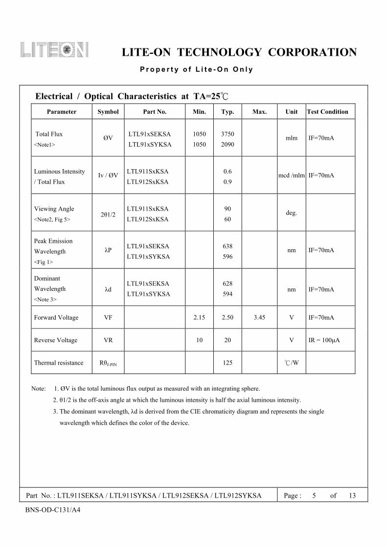
Electrical / Optical Characteristics at TA=25℃ Parameter Symbol Part No. Min. Typ. Max. Unit Test Condition
Total Flux <Note1>
ØV LTL91xSEKSA LTL91xSYKSA
1050 1050
3750 2090
mlm IF=70mA
Luminous Intensity / Total Flux
Iv / ØV LTL911SxKSA LTL912SxKSA
0.6 0.9
mcd /mlm IF=70mA
Viewing Angle <Note2, Fig 5>
2θ1/2 LTL911SxKSA LTL912SxKSA
90 60
deg.
Peak Emission Wavelength <Fig 1>
λP LTL91xSEKSA LTL91xSYKSA
638 596
nm IF=70mA
Dominant Wavelength <Note 3>
λd LTL91xSEKSA LTL91xSYKSA
628 594
nm IF=70mA
Forward Voltage VF 2.15 2.50 3.45 V IF=70mA
Reverse Voltage VR 10 20 V IR = 100µA
Thermal resistance RθJ-PIN 125 /W℃
Note: 1. ØV is the total luminous flux output as measured with an integrating sphere.
2. θ1/2 is the off-axis angle at which the luminous intensity is half the axial luminous intensity.
3. The dominant wavelength, λd is derived from the CIE chromaticity diagram and represents the single
wavelength which defines the color of the device.
Part No. : LTL911SEKSA / LTL911SYKSA / LTL912SEKSA / LTL912SYKSA Page : 5 of 13
BNS-OD-C131/A4
LITE-ON TECHNOLOGY ORPORATION P r o p e r t y o f L i t e - O n O n l y
Part No. : LTL911SEKSA / LTL911SYKSA / LTL912SEKSA / LTL912SYKSA Page : 9 of 13
BNS-OD-C131/A4
LITE-ON TECHNOLOGY ORPORATION P r o p e r t y o f L i t e - O n O n l y
CAUTIONS 1. Application
The LEDs described here are intended to be used for ordinary electronic equipment (such as office equipment, communication equipment and household applications).Consult Liteon’s Sales in advance for information on applications in which exceptional reliability is required, particularly when the failure or malfunction of the LEDs may directly jeopardize life or health (such as in aviation, transportation, traffic control equipment, medical and life support systems and safety devices).
2. Storage The storage ambient for the LEDs should not exceed 30°C temperature or 70% relative humidity. It is recommended that LEDs out of their original packaging are used within three months. For extended storage out of their original packaging, it is recommended that the LEDs be stored in a sealed container with appropriate desiccant or in desiccators with nitrogen ambient.
3. Cleaning Use alcohol-based cleaning solvents such as isopropyl alcohol to clean the LEDs if necessary.
4. Lead Forming & Assembly
During lead forming, the leads should be bent at a point at least 3mm from the base of LED lens.
Do not use the base of the lead frame as a fulcrum during forming.
Lead forming must be done before soldering, at normal temperature. During assembly on PCB, use minimum clinch force possible to avoid excessive mechanical stress.
5. Soldering When soldering, leave a minimum of 2mm clearance from the base of the lens to the soldering point.
Dipping the lens into the solder must be avoided. Do not apply any external stress to the lead frame during soldering while the LED is at high temperature. Recommended soldering conditions :
Soldering iron Wave soldering
Temperature Soldering time
300°C Max. 3 sec. Max. (one time only)
Pre-heat Pre-heat time Solder wave Soldering time
100°C Max. 30 sec. Max. 260°C Max. 5 sec. Max.
Note: Excessive soldering temperature and/or time might result in deformation of the LED lens or catastrophic failure of the LED
Part No. : LTL911SEKSA / LTL911SYKSA / LTL912SEKSA / LTL912SYKSA Page : 10 of 13
BNS-OD-C131/A4
LITE-ON TECHNOLOGY ORPORATION P r o p e r t y o f L i t e - O n O n l y
6. Drive Method An LED is a current-operated device. In order to ensure intensity uniformity on multiple LEDs connected in parallel in an application, it is recommended that a current limiting resistor be incorporated in the drive circuit, in series with each LED as shown in Circuit A below.
Circuit model A Circuit model B
LED
LED
(A) Recommended circuit
(B) The brightness of each LED might appear different due to the differences in the I-V characteristics of those LEDs
7. ESD (Electrostatic Discharge) Static Electricity or power surge will damage the LED. Suggestions to prevent ESD damage:
Use a conductive wrist band or anti- electrostatic glove when handling these LEDs All devices, equipment, and machinery must be properly grounded Work tables, storage racks, etc. should be properly grounded Use ion blower to neutralize the static charge which might have built up on surface of the LEDs plastic lens as a result of friction between LEDs during storage and handing
ESD-damaged Leeds will exhibit abnormal characteristics such as high reverse leakage current, low forward voltage, or “no light up” at low currents. To verify for ESD damage, check for “light up” and Vf of the suspect LEDs at low currents.
Part No. : LTL911SEKSA / LTL911SYKSA / LTL912SEKSA / LTL912SYKSA Page : 11 of 13
BNS-OD-C131/A4
Chip ESD level Machine Model Human Body Model
I InGaN / Sapphire 100 V 300 V
AlInGaP 200 V 500 V
InGaN / SiC 600 V 1000 V
LITE-ON TECHNOLOGY ORPORATION P r o p e r t y o f L i t e - O n O n l y
Suggested checking list :
Training and Certification 1. Everyone working in a static-safe area is ESD-certified? 2. Training records kept and re-certification dates monitored? Static-Safe Workstation & Work Areas 1. Static-safe workstation or work-areas have ESD signs? 2. All surfaces and objects at all static-safe workstation and within 1 ft measure less than 100V? 3. All ionizer activated, positioned towards the units? 4. Each work surface mats grounding is good? Personnel Grounding 1. Every person (including visitors) handling ESD sensitive (ESDS) items wear wrist strap, heel strap or
conductive shoes with conductive flooring? 2. If conductive footwear used, conductive flooring also present where operator stand or walk? 3. Garments, hairs or anything closer than 1 ft to ESD items measure less than 100V*? 4. Every wrist strap or heel strap/conductive shoes checked daily and result recorded for all DSL? 5. All wrist strap or heel strap checkers calibration up to date? Note: *50V for Blue LED. Device Handling 1. Every ESDS items identified by EIA-471 labels on item or packaging?
2. All ESDS items completely inside properly closed static-shielding containers when not at static-safe workstation?
3. No static charge generators (e.g. plastics) inside shielding containers with ESDS items? 4. All flexible conductive and dissipative package materials inspected before reuse or recycle? Others 1. Audit result reported to entity ESD control coordinator? 2. Corrective action from previous audits completed?
3. Are audit records complete and on file?
Part No. : LTL911SEKSA / LTL911SYKSA / LTL912SEKSA / LTL912SYKSA Page : 12 of 13
BNS-OD-C131/A4
LITE-ON TECHNOLOGY ORPORATION P r o p e r t y o f L i t e - O n O n l y
8. Reliability Test
Classification Test Item Test Condition Reference Standard
Operation Life Ta= Under Room Temperature As Per Data Sheet Maximum Rating *Test Time= 1000HRS (-24HRS,+72HRS)
MIL-STD-750D:1026 (1995) MIL-STD-883D:1005 (1991) JIS C 7021:B-1 (1982)
High Temperature High Humidity Storage
Ta= 65±5℃ RH= 90 〜 95% Test Time= 240HRS±2HRS
MIL-STD-202F: 103B(1980) JIS C 7021 : B-11(1982)
High Temperature High Humidity Reverse BIAS
Ta= 85℃ RH= 85% VR=5V Test Time = 1000HRS (-24HRS, +48HRS)
Solderability T. sol = 230 ± 5℃ Dwell Time= 5 ± 1secs
MIL-STD-202F:208D(1980) MIL-STD-750D:2026(1995) MIL-STD-883D:2003(1991) JIS C 7021: A-2(1982)
9. Others The appearance and specifications of the product may be modified for improvement, without prior notice. Liteon may make process or materials changes affecting the performance or other characteristics of our
products. These products supplied after such changes will continue to meet published specifications, but may not be identical to products supplied as samples or under prior orders.
Part No. : LTL911SEKSA / LTL911SYKSA / LTL912SEKSA / LTL912SYKSA Page : 13 of 13