LITHOGRAPHY LANDSCAPE Introduction Over the past 30 years, minimum fea- ture sizes for advanced integrated circuits have been reduced by over 100X, from several microns in the early 1980s to just 32 nm today, with plans for sub-20 nm production firmly in place at most major manufacturers. While predictions abound that the relentless pace of geometry shrinks will have to end at some point, it seems clear the industry is well on target to continue shrinking geometries to less than 10 nm before the end of the decade. What is less clear is which lithographic technology will be used in producing these leading-edge devices. There is currently no single solution that is proven to meet both the technical and economic requirements for volume manufacturing below 20 nm.[1] Roadmaps exist for multiple competing solutions, but the process of selecting a viable manufacturing solution takes far more than a roadmap. In the past, key technology inflection points have been decided by an industry- wide consensus, with one clear winner emerging from among a group of compet- ing alternatives to gain widespread adop- tion. In optical lithography, prime examples of this have been the adoption of 248 nm excimer laser tools, followed by 193 nm and 193 nm immersion (193i). Competing alternatives such as 157 nm, despite years of development, failed to gain even limited adoption. In the technology arena of next-generation lithography (NGL), only extreme ultraviolet lithography (EUV) has survived as a valid candidate for HVM insertion. e-beam projection (EPL), optical maskless (OML), 1x X-ray and ion beam lithography (IBL), to name a few, have fall- en off the roadmap over the past decade. It would be tempting to conclude that history shows there can be only one win- ner at each inflection point, and that single chosen technology must therefore be adopted by all segments of the industry that wish to stay on the path of Moore’s Law. As we look to the future below 20 nm, however, many in the industry feel that “one size fits all” is no longer a viable model for all use cases. Today we see numerous competing options that are favored by one segment or another, and a growing number of lithography strategists have begun to consider the real possibility that different choices will emerge as being best for different applications. Instead of The Need for Multiple Alternatives for sub-20 nm Lithography Moshe Preil GLOBALFOUNDRIES FUTURE FAB International | Issue 38
Transcript
LITHOGRAPHY LANDSCAPE
IntroductionOver the past 30 years, minimum fea-
ture sizes for advanced integrated circuitshave been reduced by over 100X, fromseveral microns in the early 1980s to just32 nm today, with plans for sub-20 nmproduction firmly in place at most majormanufacturers. While predictions aboundthat the relentless pace of geometryshrinks will have to end at some point, itseems clear the industry is well on targetto continue shrinking geometries to lessthan 10 nm before the end of the decade.What is less clear is which lithographictechnology will be used in producing theseleading-edge devices. There is currently nosingle solution that is proven to meet boththe technical and economic requirementsfor volume manufacturing below 20 nm.[1]Roadmaps exist for multiple competingsolutions, but the process of selecting aviable manufacturing solution takes farmore than a roadmap.
In the past, key technology inflectionpoints have been decided by an industry-wide consensus, with one clear winneremerging from among a group of compet-ing alternatives to gain widespread adop-tion. In optical lithography, prime examples
of this have been the adoption of 248 nmexcimer laser tools, followed by 193 nmand 193 nm immersion (193i). Competingalternatives such as 157 nm, despite yearsof development, failed to gain even limitedadoption. In the technology arena of next-generation lithography (NGL), onlyextreme ultraviolet lithography (EUV) hassurvived as a valid candidate for HVMinsertion. e-beam projection (EPL), opticalmaskless (OML), 1x X-ray and ion beamlithography (IBL), to name a few, have fall-en off the roadmap over the past decade.
It would be tempting to conclude thathistory shows there can be only one win-ner at each inflection point, and that singlechosen technology must therefore beadopted by all segments of the industrythat wish to stay on the path of Moore’sLaw. As we look to the future below 20nm, however, many in the industry feel that “one size fits all” is no longer a viablemodel for all use cases. Today we seenumerous competing options that arefavored by one segment or another, and agrowing number of lithography strategistshave begun to consider the real possibilitythat different choices will emerge as beingbest for different applications. Instead of
The Need for Multiple Alternatives for sub-20 nm LithographyMoshe Preil GLOBALFOUNDRIES
FUTURE FAB International | Issue 38
LITHOGRAPHY LANDSCAPE
one size fits all, we are seeing the begin-ning of custom-tailored solutions. In thispaper, we will explore the economic andtechnical reasons for this change and pro-pose that the industry can and should bemore open to multiple complementarysolutions rather than the winner-take-allapproach of previous technology cycles.
Historical Survey of Past Inflection Points
To gain some perspective on the evol-ution of lithography options, it is worth taking a brief survey of past industrywidetransitions (Figure 1). While the exactdates when a specific technology was first used for high-volume manufacturing(HVM) and when that technology became
the dominant choice are always subject todebate, the general trend is clear. At eachmajor changeover point, one and only onenew technology successfully transitionedfrom lab to fab to become the industry-wide technology of choice for leading-edge production.
For every roadmap winner, however,there have always been multiple technolo-gies that were not adopted by any sizablesegment of the industry. Between the intro-duction of 193 nm dry and immersion litho-graphies, extensive development resourceswere invested in 157 nm. Scanners weredesigned and constructed, entire factorieswere built to produce lithographic gradeoptical materials, and new fluorine-basedresist chemistries were developed before
500
450
400
350
300
250
200
150
1980 1985 1990 1995 2000 2005 2010 2015 2020
100
50
0
EUV
193i
193 nm
DUV
i-line
g-line
Figure 1. Trend in Leading-Edge Lithography Wavelength Vs. Time
www.future-fab.com
the technology was abandoned in 2003.Several years later, high-index 193 nmimmersion was under serious considerationbefore being shelved in late 2008. Finally,multiple alternatives to EUV were consid-ered and actively debated in a series ofindustrywide NGL forums and their succes-sors from 1997 to the present. Despitestrong advocacy by the champions of eachtechnology and years of impressive presen-tations and data, only EUV has survived tostand today at the threshold of insertioninto manufacturing.
This trail of technology roadkill wouldseem to suggest there are fundamentalreasons the industry can only support onenew lithography option every five to sevenyears. If this “rule” were applied to the2013-2020 time frame, it would seem toimply that only EUV can succeed as a new HVM technology for the rest of thisdecade, given how far along EUV is on theroad to commercialization and how far anyalternative is from production readiness.The only other option would be to staywith 193 nm immersion and move to threeor more masks per layer (pitch splitting),which would drastically increase the costof manufacturing due to the proliferationof masking steps, critical masks, andreduced overlay and CD control budgetsper exposure. It would also vastly compli-cate the task of circuit layout and design,making it inaccessible to many end-usersand sharply reducing the available marketfor new designs.
Before accepting this as an inevitableconclusion, it would be instructive to lookbeyond simple extrapolation and ask,“What are the underlying reasons for thispast experience, and do these reasons stillhold true for today’s competing technologyoptions”? The key points that doomed pasttechnology also-rans were the lack of ade-
quate infrastructure and the reluctance ofthe industry to fund that infrastructure dueto limited extendibility of the technology.Without a viable ecosystem to deliver everyneeded element of the new technology,building an exposure tool alone proved tobe insufficient, and funding for the toolswas eventually terminated. Table 1 lists themost critical missing links for some of theabandoned options of the recent past.
There are, to be sure, those who wouldargue that EUV still faces daunting infra-structure challenges of its own; sourceswith adequate power to enable high-throughput operation, defect-free maskblanks, a proven vacuum-compatible maskhandling and storage system to keep themask clean over time without a pellicle,and affordable actinic wavelength maskinspection capability. In fact, the hugeinvestment being made to develop a viableEUV infrastructure is often cited as a majorreason for the lack of funding for otherpotential candidates. The frequently heardcomment, “If we only had 10 percent of themoney that was invested in EUV we couldhave solved all of our problems by now,”has been heard from more than one com-peting technology champion. Nonetheless,the fact remains that EUV is firmly on thepath to commercialization. It has literallybecome too big to fail.
But this does not mean that EUV will bethe only choice for the next several nodes.It only means that any other technologymust not require any major new infrastruc-ture investment. In this respect, we mustconsider the EDA world and design con-straints as part of the technology ecosys-tem that would need to be reused. In thefollowing sections, we will consider thecost/benefit trade-offs of several compet-ing options and demonstrate their viabilitynot as direct competitors to displace EUV,
The Need for Multiple Alternatives for sub-20 nm Lithography
FUTURE FAB International | Issue 38
but rather as complementary tools to create cost-effective solutions for differentsegments of the industry.
Alternatives for sub-20 nm Lithography
The 2010 ITRS roadmap[1] predicts theadoption of sub-20 nm technology in 2016,with minimum half-pitches of 23 nm forDRAM, 19 nm for MPU and ASIC metal layers and 16 nm for flash memory. Theoptions still listed as being under considera-tion are 193 nm immersion with multiple pat-
terning (DPT), EUV, imprint, direct write(often referred to as maskless lithography, orML2) and 193 nm immersion with directedself-assembly (DSA). The leading option forML2 remains e-beam direct write (EBDW)although optical and hybrid opto-electronictools have also been proposed. As usual,major IC manufacturers are already predict-ing they will begin production of this nodesignificantly ahead of the roadmap and/or at even smaller geometries.
The design constraints imposed by different industry segments play a critical
LITHOGRAPHY LANDSCAPE
No proven optical solution below this line
First Year of IC Production 2009 2010 2011 2012 2013 2014 2015 2016 2017 2018 2019 2020 2021 2022
role in developing and implementing a cost-effective lithography strategy.Memory can push to the tightest possiblepitch and take advantage of novel tech-niques that print perfectly regular arrays of lines and spaces. Integrated devicemanufacturers (IDM) with a small numberof high-volume, high-value products suchas microprocessors have the ability toimpose very restrictive design rules andwork closely with the designers to co-optimize the process and design. In thefoundry arena, the huge number of designsand customers requires the most robustprocesses that will yield working die forthousands of different products runningmany different flavors of the base process.
In addition to adopting different levelsof layout constraints and design-processco-optimization, these industry segmentsare also under different levels of econom-ic pressure in dealing with the soaringcost of masks. A multimillion-dollar maskset that produces millions of high-valueCPU or PLD chips adds only a small per-centage of the cost per die; that samemask cost adds an unsupportable burdento the cost per die of a low-volume ASIC.On the other hand, reducing throughputby moving to maskless lithography ormultiple patterning may be cost-effective
for low-volume parts but would be unableto manufacture memory or CPU chips insufficient volume. Memory and logic alsodiverge in terms of defect tolerance. Thebuilt-in redundancy in memory chipsallows more compromise in terms ofmask and wafer defectivity than complexlogic devices.
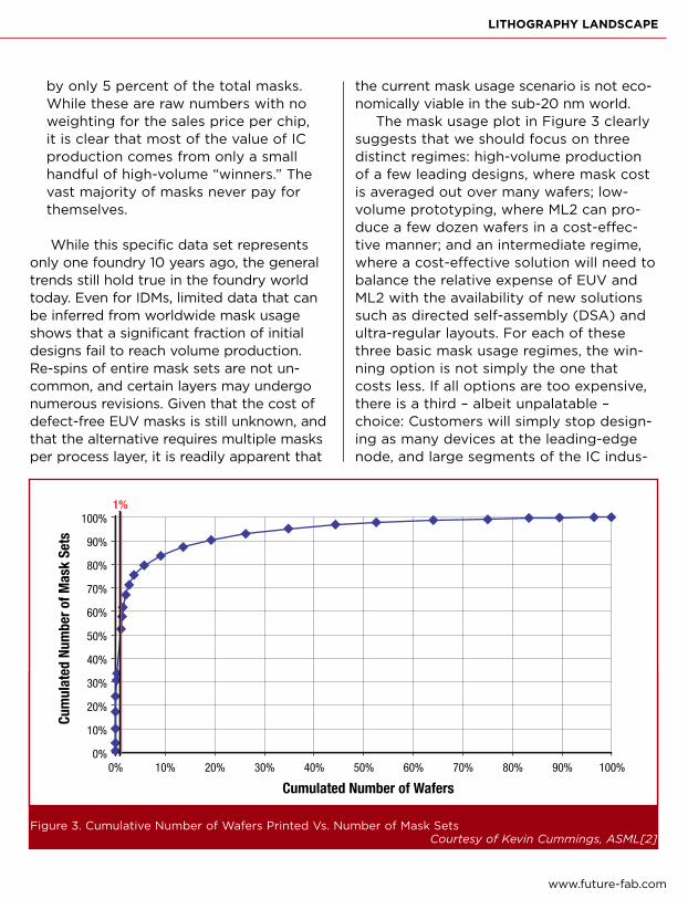
The issue of mask costs is further com-plicated by the low percentage of masksthat actually result in profitable, high-volume device production. Actual data onwafers produced per mask is notoriouslywell protected for commercial reasons.One study,[2] published in 2002, is shownin Figure 3. This data showed the maskusage dilemma with striking clarity:• Over 50 percent of the masks produced
only 1 percent of all wafers in thefoundry environment.
• The mean number of wafers per maskwas roughly 700. However, the mediannumber was even lower, at barely 100wafers per mask. It is the median num-ber that truly reflects the severity of theproblem since the mean is inflated by avery small number of highly successfuldevices.
• Over 80 percent of the wafers wereprinted by just 10 percent of the masks;65 percent of the wafers were printed
The Need for Multiple Alternatives for sub-20 nm Lithography
Alternate: stencil masks• Also fragile• Cannot print isolated solidstructures
Mask heating and distortionissues at required throughput
1X membrane masks• Defect, overlay and CDrequirements at 1X• Membrane mask distortion• Fragile• Seemed viable when firstproposed for 1 micron, couldnot meet tighter specs < 250 nm
High-index glass material• Availability in sufficientquality and quantity
Fragile membrane masks
High-index resist materials
High-index fluids
No immersion medium (waterdoesn’t work)• Limited extendibility
CaF2 supply issues
Pellicle issues (hard pelliclerequired)
157 nm High-Index 193i EPL 1X X-ray
Table 1. Key Infrastructure Issues in Previous Unadopted Technologies
FUTURE FAB International | Issue 38
by only 5 percent of the total masks.While these are raw numbers with noweighting for the sales price per chip, it is clear that most of the value of ICproduction comes from only a smallhandful of high-volume “winners.” Thevast majority of masks never pay forthemselves.
While this specific data set representsonly one foundry 10 years ago, the generaltrends still hold true in the foundry worldtoday. Even for IDMs, limited data that canbe inferred from worldwide mask usageshows that a significant fraction of initialdesigns fail to reach volume production. Re-spins of entire mask sets are not un-common, and certain layers may undergonumerous revisions. Given that the cost ofdefect-free EUV masks is still unknown, andthat the alternative requires multiple masksper process layer, it is readily apparent that
the current mask usage scenario is not eco-nomically viable in the sub-20 nm world.
The mask usage plot in Figure 3 clearlysuggests that we should focus on threedistinct regimes: high-volume productionof a few leading designs, where mask costis averaged out over many wafers; low-volume prototyping, where ML2 can pro-duce a few dozen wafers in a cost-effec-tive manner; and an intermediate regime,where a cost-effective solution will need tobalance the relative expense of EUV andML2 with the availability of new solutionssuch as directed self-assembly (DSA) andultra-regular layouts. For each of thesethree basic mask usage regimes, the win-ning option is not simply the one thatcosts less. If all options are too expensive,there is a third – albeit unpalatable –choice: Customers will simply stop design-ing as many devices at the leading-edgenode, and large segments of the IC indus-
LITHOGRAPHY LANDSCAPE
0%
10%
0%
1%
10% 20% 30% 40%
Cumulated Number of Wafers
Cum
ulat
ed N
umbe
r of M
ask
Sets
50% 60% 70% 80% 90% 100%
20%
30%
40%
50%
60%
70%
80%
90%
100%
Figure 3. Cumulative Number of Wafers Printed Vs. Number of Mask Sets Courtesy of Kevin Cummings, ASML[2]
www.future-fab.com
try will transition from high growth tomature, steady-state businesses. To pre-vent economics from bringing Moore’s Lawto a premature end, we must consider howdifferent strategies can be optimized foreach of the three mask usage regimes and not force one solution onto three usecases with very different cost models.
The Case for ComplementaryTechnologies: ML2 + EUV
Maskless lithography has often beenproposed as a replacement technology forexpensive mask-based approaches,[3,4]but the low throughput of any proposedML2 exposure tool makes this impracticalfor high-volume production. As long as weregard ML2 and EUV as competitors in a winner-take-all battle, there can be noclear winner. An obvious solution to
this dilemma is to develop a moderate-throughput, low-cost EBDW tool that is a complement, not a competitor, to themore expensive, high-volume optical andEUV exposure tools.
While the concept of using ML2 for prototyping has been proposed numeroustimes in the past, the maskless exposuretools available to date have not met theresolution and throughput requirementseven for this specialized use case. Single-column direct-write e-beam tools currentlyproduce one to two wafers per day, notthe several wafers per hour required.Several tools now under developmentshow promise for delivering five-20 wafersper hour (WPH), which would be adequatefor a low-cost prototyping tool. Even atjust five WPH, a $20 million ML2 toolwould be more cost-effective than a larger,
The Need for Multiple Alternatives for sub-20 nm Lithography
0
500
0 5 10 15
Mask Cost $50K
Mask Cost $100K
Mask Cost $200K
20
1000
1500
2000
2500
ML2 Throughput (WPH)
ML2
Bre
akev
en (W
afer
s/M
ask)
ML2 Breakeven vs. Mask Cost and ML2 ThroughputAssumptions: Scanner = $75M, 150 WPH, ML2 = $20M
Figure 4. Maskless vs. mask-based breakeven as a function of EUV mask cost and ML2 throughput.Assumed tools costs and EUV throughput are fixed in this example.
FUTURE FAB International | Issue 38
more expensive EUV tool running 10-20Xthe throughput with a mask cost measuredon the order of $100,000.
Figure 4 shows a sample trade-offbetween ML2 and EUV over a range ofassumptions for ML2 throughput and EUVmask cost; other parameters that werefixed in this example are listed in the fig-ure. The key performance indicator plottedhere is the breakeven number of wafersper mask. If the mask is used for morethan this number of wafers, mask-basedlithography is cheaper; less than this valueand ML2 is more cost-effective. This simplemodel shows that a 10 WPH, $20 millionmaskless tool would reach breakeven witha $75 million 150 WPH EUV tool and amask cost of $200,000 at about 2,300wafers per mask. Clearly we would notbother to incur the expense of masklessprototyping if the actual number ofwafers/mask was even close to thebreakeven point. However, as shown inFigure 4, a very large number of masks areused less than one-tenth as many times,making maskless prototyping a significantcost savings strategy. The cost of equip-ping a fab with several small, low-cost ML2exposure tools will be offset many timesover by the huge cost savings of not pro-ducing hundreds of expensive EUV (orDPT) masks that are used a limited number of times and discarded.
A key factor in this complementaryscheme is to recognize that the masklessexposure tool must mimic the patterningperformance of the high-volume tool. Thisis a non-trivial constraint that has not beenwidely applied to maskless tools in thepast. Rather than trying to push the ML2tool to print the squarest line ends andcontact holes possible, care must be takento emulate the actual rounding and prox-imity effects that will occur in the optical
process once the design passes the proto-type phase and moves to high-volume pro-duction. This may seem to be imposing anunfair burden on the ML2 tool that wouldnot be necessary in a purely masklessapplication, but it is a critical requirementfor a successful complementary strategy.Early discussions with several candidatesuppliers have shown that this constraintcan be met through extensive simulation,data handling and beam control compu-tation currently under development.
The Case for Complementary Technologies: Ultra-Regular Layouts
Another emerging opportunity for multi-ple technologies to work together is to use amask-based tool to print an ultra-regular 1Darray of lines and spaces at a single pitch,then follow up with a maskless tool to cutthe lines into a usable device layout (seeFigure 5).[5] This concept has been dis-cussed for close to 10 years but, as withmany novel ideas, has not been widelyadopted yet due to the relentless progressof optical lithography. With optical now run-ning up against the physical limits of numeri-cal aperture and wavelength, as well as theeconomic limits of mask and tool costs, thishybrid approach has gained significant trac-tion, especially since it was promoted by YanBorodovsky of Intel at SPIE in early 2010.
The initial grating pattern can be formedby several different technologies. 193i withsome type of frequency multiplication –either multiple patterning technology ordirected self-assembly – would enable us toprint gratings as small as 15 nm half-pitch.The first generation of EUV productiontools could lower this to just 14 nm, andEUV plus multiple patterning or DSA mightwell take us under 10 nm. Bear in mind thatthese are actual grating pitches, not node
LITHOGRAPHY LANDSCAPE
www.future-fab.com
names, and could therefore meet therequirements of logic device manufacturingas far as the 6 nm node in 2021.
The clear advantage of such a comple-mentary approach is the dramatic reduc-tion in the number of masks needed. In themask usage plot (Figure 2), the cut layerapproach would help in all three regimes:• Low-volume prototyping – this
approach would eliminate a large per-centage of the masks wasted due todesign re-spins. Even if the initial devicedoes not work, the redesign could bedone entirely by modifying the direct-write cut layers without requiring anynew masks.
• High-volume regime – this approachwould require fewer masks for layersrequiring multiple patterning.
• Mid-volume region – it would be prefer-able to use 193i and extensive cutmasks rather than absorbing the cost ofbuilding EUV masks for devices that arenot expected to be manufactured bythe millions. It is even conceivable –though admittedly a remote option -that multiple designs could be closeenough in terms of die size to share asingle grating mask and simply trim thedie differently.
On the other hand, implementing ultra-regular layouts shifts the burden frommask costs to design constraints. WhileIDMs may still have the luxury of largedesign and process teams working closelytogether to customize each design andcell, in the fables-foundry model, this is nota supportable way of working. The abilityof the electronic design automation (EDA)community to implement software toolsthat can lay out any required cell on apurely one-dimensional array without anexcessive die size penalty will be a keyenabling technology for the adoption ofcost effective complementary lithography.
e-beam Direct WriteConsiderations forComplementary Lithography
One of the critical limitations of EBDW is the finite number of electrons that can begenerated and moved through the electronoptics without excessive beam blur due to Coulomb repulsion.[7-9] At the largergeometries used for mask making, this limit-ation has previously been met by using moresensitive resists with target doses in the rangeof 5-20 µC/cm2. For wafer-level geometries,however (and even for leading-edge masks),it is no longer possible to use such fast resists
The Need for Multiple Alternatives for sub-20 nm Lithography
Figure 5. Complementary lithography using ultra-regular arrays and cut masks.[5] Four separate maskswould be required if the cuts were all done with 193 nm lithography. This can be reduced to one maskusing EUV or none with direct write.
Courtesy Yan Borodovsky, LithoVision 2010, February 21, 2010 San Jose, CA, USA
FUTURE FAB International | Issue 38
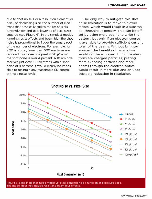
due to shot noise. For a resolution element, orpixel, of decreasing size, the number of elec-trons that physically strikes the resist is dis-turbingly low and gets lower as 1/(pixel size)squared (see Figure 6). In the simplest model,ignoring resist effects and beam blur, the shotnoise is proportional to 1 over the square rootof the number of electrons. For example, for a 20 nm pixel, fewer than 500 electrons arerequired to expose one pixel at 20 µC/cm2;the shot noise is over 4 percent. A 10 nm pixelreceives just over 100 electrons with a shotnoise of 9 percent. It would clearly be impos-sible to maintain any reasonable CD controlat these noise levels.
The only way to mitigate this shotnoise limitation is to move to slowerresists, which would result in a substan-tial throughput penalty. This can be off-set by using more beams to write thepattern, but only if an electron source is available to provide sufficient currentto all of the beams. Without brightersources, the benefits of parallelismwould not be achieved. But since elec-trons are charged particles, puttingmore exposing particles and morebeams through the electron opticswould result in more blur and an unac-ceptable reduction in resolution.
LITHOGRAPHY LANDSCAPE
5
Pixel Dimension (nm)
0.1%
0.2%
0.4%
0.8%
1.6%
3.1%
6.3%
12.5%
25.0%
Shot
Noi
se
Shot Noise vs. Pixel Size
50
10 µC/ cm2
1 µC/ cm2
20 µC/ cm2
50 µC/ cm2
100 µC/ cm2
150 µC/ cm2
200 µC/ cm2
500 µC/ cm2
1000 µC/ cm2
Figure 6. Simplified shot noise model vs. pixel dimension as a function of exposure dose. The model does not include resist and beam blur effects.
www.future-fab.com
The cut mask approach is particularlywell suited to a single-column, multiple-beam design. Since only a few pixels wouldbe written simultaneously, the maximumbeam current allowed would be divided by relatively few beams, enabling higher dose writing while maintaining adequatethroughput. This particular design advan-tage has been recognized by KLA-Tencor in their proposed REBL system.[10] Thethroughput of this tool for writing a sparsepattern such as a cut mask could be up to5X higher than trying to write a dense arrayof line/space patterns. A competing con-cept embodied by the MAPPER system[11]uses one beam source but many microma-chined columns. The current per column is thus kept at a manageable level for any pattern density. The raster scanningapproach required for a multicolumn arrayprovides the same throughput regardless of pattern density. Such trade-offs betweensystem design, cost and intended use casewill become increasingly critical as thesetechnologies get closer to production. It is not unreasonable to think they will eachplay a role in different applications.
ConclusionsWhile EUV will be the mainstream tech-
nology of choice for the highest-volumeproducts below the 20 nm node, othertechnologies will be necessary to comple-ment EUV in a cost-effective mode. Direct-write technologies and ultra-regular 1Xarrays patterned by DSA, multiple pattern-ing or EUV will all be part of the mix.Rather than engaging in fratricidal comp-etition to determine a single winner, itwould benefit the industry to put moreeffort into making these different techno-logies work together to deliver cost-effec-tive solutions for all segments of the indus-try. Developing complementary lithography
technologies will require the developmentof new exposure tools, new EDA tools andnew strategies to mix exposures betweenthese different tools. While this new way of working may not be as appealing toinvestors hoping for a winner-take-all wind-fall, the alternative could well be the end ofaffordable scaling and a lose-lose situationfor suppliers and IC manufacturers alike.
Endnotes1. International Technology Roadmap for
Semiconductors2. K. Cummings, “A business perspective
for maskless lithography,” BACUS PanelSession, September 2003.
3. R. Pease et al. “Distributed Axis FixedAperture (DIFA) Electron BeamTechnology,” International SEMATECHLithography Forum, January 2004.
4. T. Chang et al. “Electron Beam Micro-columns for lithography and relatedapplications,” J. Vac. Sci. Technol.B14(6), 3774 (1996).
5. Y. Borodovsky, “ArF LithographyExtension for Critical Layer Patterning,”Nikon LithoVision seminar, 2010
6. This value is used for illustration onlyand is not intended to represent anyspecific exposure system.
7. A. Neureuther et al. “Shot noise modelsfor sequential processes and the role oflateral mixing,” J. Vac. Sci. Technol. B24, 1902 (2006).
8. P. Kruit et al. “Optimum dose for shotnoise limited CD uniformity in electron-beam lithography,” J. Vac. Sci. Technol.B 22(6), 2948 (2004).
9. N. Rau et al. “Shot-noise and edgeroughness effects in resists patternedat 10 nm exposure,” J. Vac. Sci. Technol.B 16 (6), 3784-3788, (1998).
10. P. Petric et al. “New advances withREBL for maskless high throughput
The Need for Multiple Alternatives for sub-20 nm Lithography
FUTURE FAB International | Issue 38
EBDW lithography,” Proc. SPIE 7970-43 (2011).
11. M. Wieland et al. “MAPPER: Highthroughput maskless lithography,” Proc. SPIE 7637-14 (2010).
AcknowledgmentsThe themes captured in this paper have
evolved over time and benefited greatlyfrom frequent discussions with the mem-bers of the Strategic Lithography Technol-ogy group at GLOBALFOUNDRIES, espe-cially Harry Levinson and Keith Standiford.The author would also like to thank YanBorodovsky of Intel, Kevin Cummings ofASML, and SEMATECH for permission toreproduce their published results.
About the Author
Moshe PreilMoshe Preil is the manager of Emerging
Lithography and Tools, part of the Strat-egic Lithography Technology departmentat GLOBALFOUNDRIES. He has over 25years of experience in both the fab andsupplier sides of the industry, working invarious lithography, process control andyield management positions. Previously at AMD, Dr. Preil was involved in the earlydevelopment of deep-UV technology. He earned his Ph.D. in physics from theUniversity of Pennsylvania, working onoptical and electron spectroscopies ofnovel graphite-based compounds. Dr. Preilhas published numerous journal papersand has been issued nine U.S. patents. �


![2 LASER INTERFERENCE LITHOGRAPHY - uni-halle.de · 2 LASER INTERFERENCE LITHOGRAPHY (LIL) 9 2 LASER INTERFERENCE LITHOGRAPHY (LIL) Laser interference lithography [3~22] (LIL) is a](https://static.documents.pub/doc/80x56/5eae180eecc7e273a41a4e88/2-laser-interference-lithography-uni-hallede-2-laser-interference-lithography.jpg)


